

Page 1
8
1
8
1
8
1
EMITTER
COLLECTOR
ANODE
CATHODE
1
2
3
4 5
6
7
8
EMITTER
COLLECTOR
ANODE
CATHODE
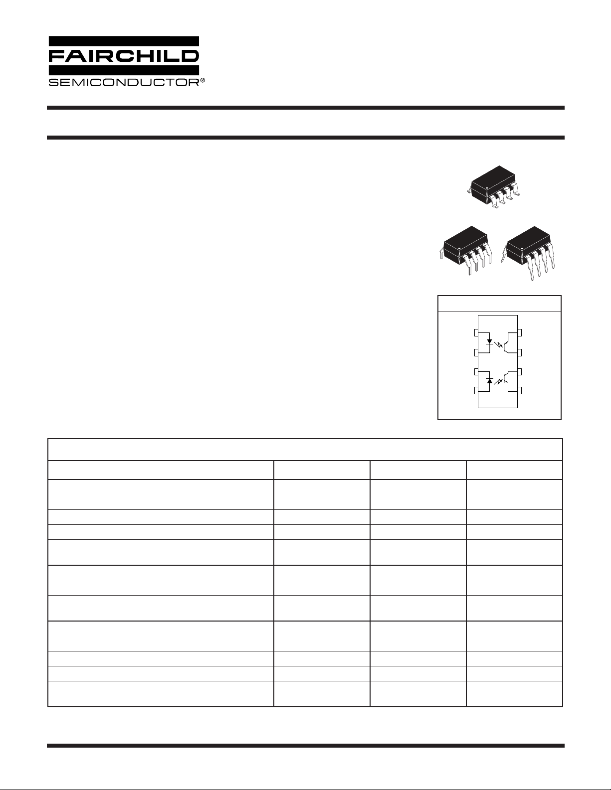
Equivalent Circuit
SCHEMATIC
DUAL PHOTOTRANSISTOR
OPTOCOUPLERS
MCT6 MCT61 MCT62
DESCRIPTION
The MCT6X Optocouplers have two channels for density applications. For four
channel applications, two-packages fit into a standard 16-pin DIP socket. Each
channel is an NPN silicon planar phototransistor optically coupled to a gallium
arsenide infrared emitting diode.
FEATURES
•Two isolated channels per package
•Two packages fit into a 16 lead DIP socket
• Choice of three current transfer ratios
• Underwriters Laboratory (U.L.) recognized File E90700
APPLICATIONS
•AC Line/Digital Logic - isolate high voltage transients
• Digital Logic/Digital Logic - Eliminate spurious grounds
• Digital Logic/AC Triac Control - isolate high voltage transients
•Twisted pair line receiver - Eliminate ground loop feedthrough
•Telephone/Telegraph line receiver - isolate high voltage transients
• High Frequency Power Supply Feedback Control - Maintain floating grounds and
transients
• Relay contact monitor - isolate floating grounds and transients
•Power supply monitor - Isolate transients
ABSOLUTE MAXIMUM RATINGS
Rating Symbol Value Unit
EMITTER (Each channel)
Forward Current - Continuous I
Forward Current - Peak (PW = 1µs, 300pps) I
Reverse Voltage V
LED Power Dissipation @ T
= 25°C
A
Derate above 25°C (Total Input)
DETECTOR (Each channel)
Collector Current - Continuous I
Detector Power Dissipation @ T
= 25°C
A
Derate above 25°C
TOTAL DEVICE
Storage Temperature T
Operating Temperature T
Lead Solder Temperature (wave solder) T
Total Device Power Dissipation @ T
Derate above 25°C
= 25°C
A
F
(pk) 3 A
F
R
P
D
C
P
D
STG
OPR
SOL
P
D
60 mA
3.0 V
100
1.3
mW
mW/°C
30 mA
150
2.0
mW
mW/°C
-55 to +150 °C
-55 to +100 °C
250 for 10 sec °C
400
5.33
mW
mW/°C
© 2003 Fairchild Semiconductor Corporation
Page 1 of 7
7/31/03
Page 2
≤
Ω
DUAL PHOTOTRANSISTOR
OPTOCOUPLERS
MCT6 MCT61 MCT62
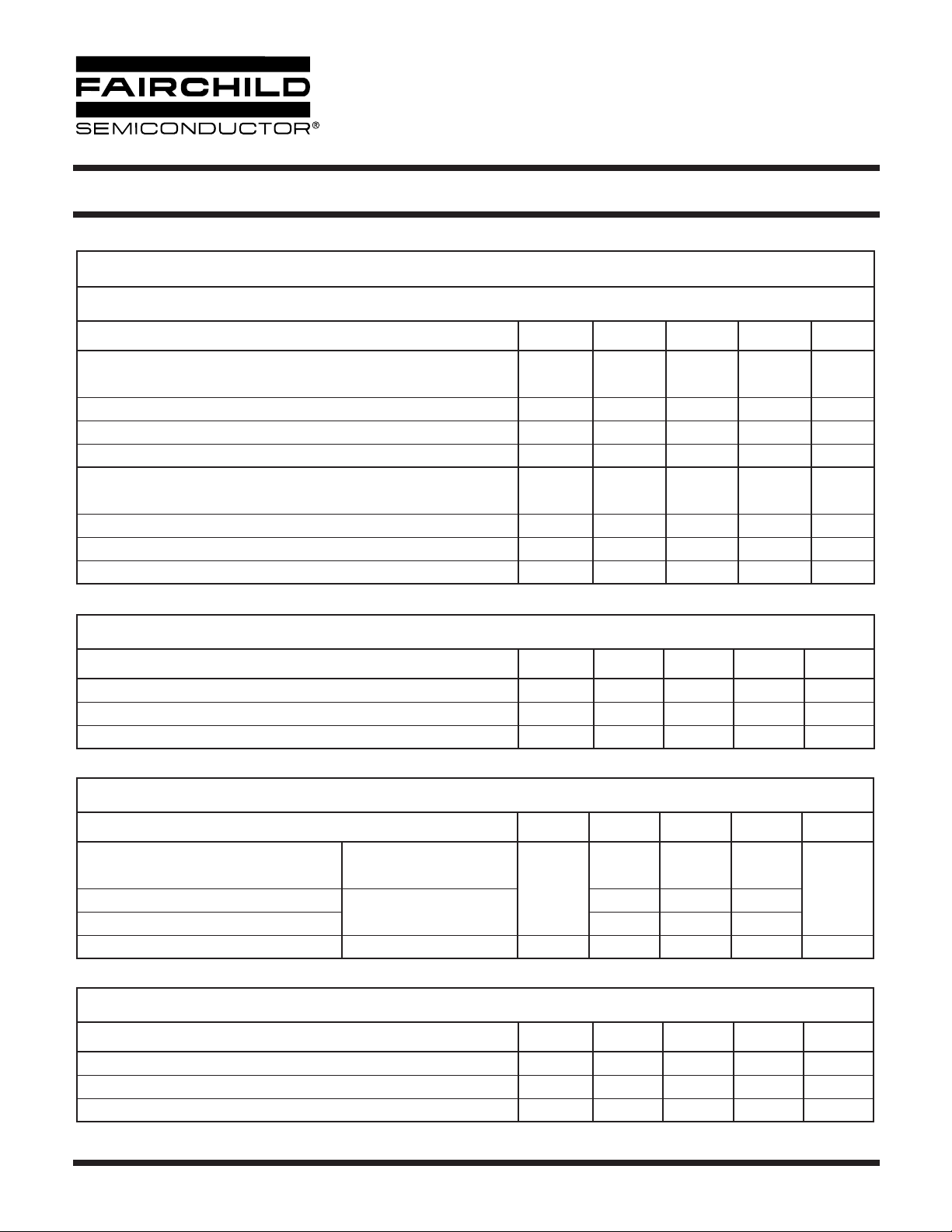
ELECTRICAL CHARACTERISTICS
(T
= 25°C Unless otherwise specified.)
A
INDIVIDUAL COMPONENT CHARACTERISTICS
Parameter Test Conditions Symbol Min Typ** Max Unit
EMITTER
Input Forward Voltage (I
Reverse Voltage (I
Reverse Current (V
Junction Capacitance (V
F
= 20 mA) V
F
= 10 µA) V
R
= 5 V) I
R
= 0 V, f = 1 MHz) C
F
R
R
J
3.0 25 V
1.2 1.5 V
0.001 10 µA
50 pF
DETECTOR
Collector-Emitter Breakdown Voltage (I
Emitter-Collector Breakdown Voltage (I
Collector-Emitter Dark Current (V
Capacitance (V
= 1.0 mA, I
C
= 100 µA, I
E
= 10 V, I
CE
= 0 V, f = 1 MHz) C
CE
= 0) BV
F
= 0) BV
F
= 0) I
F
CEO
ECO
CEO
CE
30 85 V
613 V
5 100 nA
8pF
TRANSFER CHARACTERISTICS
AC Characteristic Test Conditions Symbol Min Typ** Max Units
SWITCHING TIMES
Non-Saturated Turn-on Time (R
Non-Saturated Turn-off Time (R
= 100 Ω , I
L
= 100 Ω , I
L
= 2 mA, V
C
= 2 mA, V
C
= 10 V) t
CC
= 10 V) t
CC
on
off
2.4 µs
2.4 µs
TRANSFER CHARACTERISTICS
DC Characteristic Test Conditions Symbol Min Typ** Max Units
Current Transfer Ratio, Collector-Emitter
MCT6 (I
MCT62 100
Saturation Voltage (I
= 10 mA, V
F
(I
= 5 mA, V
F
= 16 mA, I
F
= 10 V) 20
CE
= 5 V)
CE
= 2 mA) V
C
CTR
CE(sat)
50
0.15 0.40 V
ISOLATION CHARACTERISTICS
Characteristic Test Conditions Symbol Min Typ** Max Units
Input-Output Isolation Voltage (I
Isolation Resistance (V
Isolation Capacitance (f = 1 MHz) C
** All typicals at TA = 25°C
© 2003 Fairchild Semiconductor Corporation
1 µA, t = 1 min.) V
I-O
= 500 VDC) R
I-O
Page 2 of 7
ISO
ISO
ISO
5300 Vac(rms)
11
10
0.5 pf
7/31/03
% MCT61
Page 3
DUAL PHOTOTRANSISTOR
OPTOCOUPLERS
MCT6 MCT61 MCT62
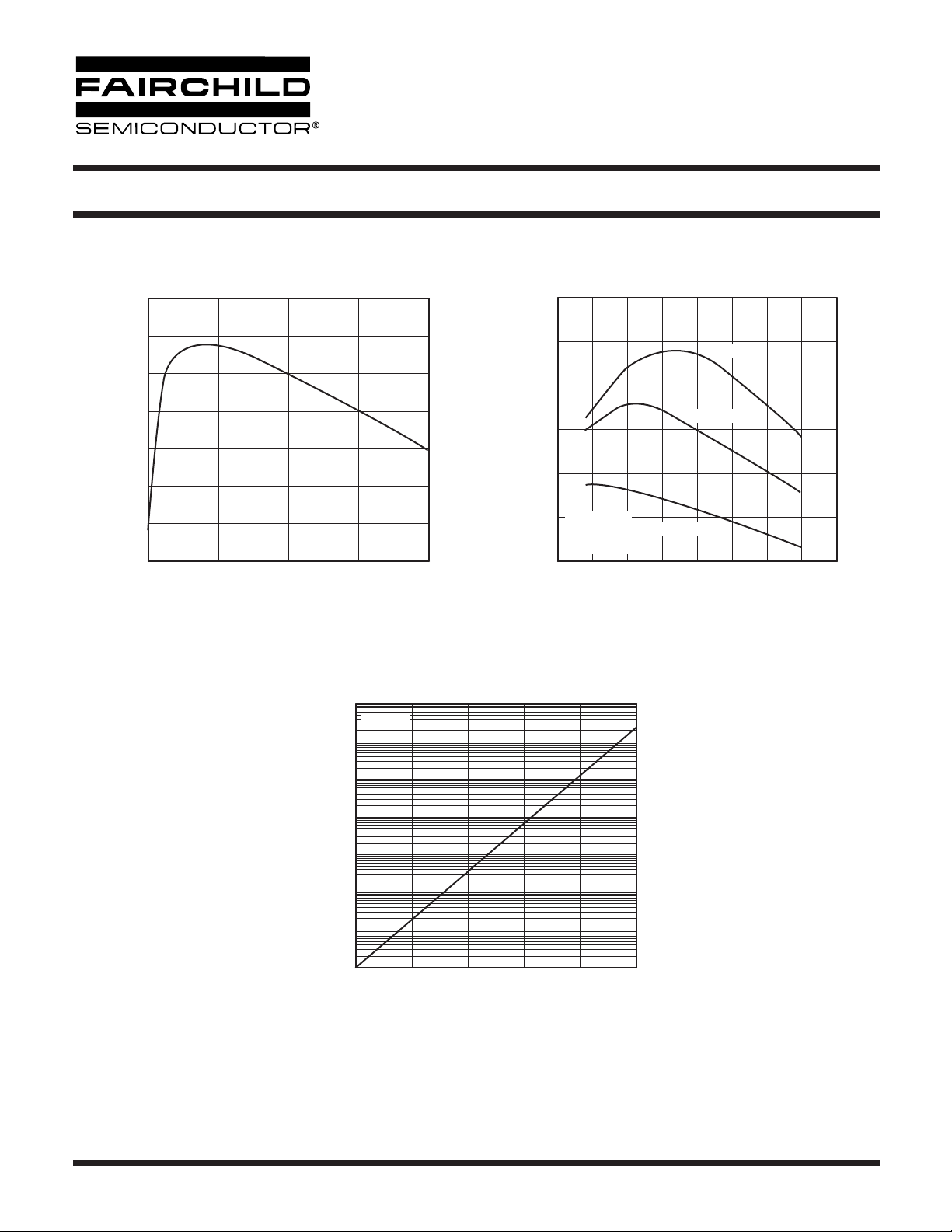
Normalized CTR vs. Forward Current
1.4
VCE = 5.0V
T
= 25˚C
A
1.2
1.0
0.8
0.6
NORMALIZED CTR
0.4
0.2
0.0
051015 20
IF - FORWARD CURRENT (mA)
1
10
VCE = 10 V
0
NT (µA)
10
Normalized to
= 10 mA
I
F
1.4
1.2
1.0
1.6
0.8
NORMALIZED CTR
0.6
0.4
-75 -50 -25 0 25 50 75 100 125
Dark Current vs. Ambient Temperature
Normalized CTR vs. Ambient Temperature
IF = 5 mA
IF = 10 mA
Normalized to
= 10 mA
I
F
= 25˚C
T
A
IF = 20 mA
TA - AMBIENT TEMPERATURE (˚C)
© 2003 Fairchild Semiconductor Corporation
-1
10
ARK CURRE
D
-2
10
-3
10
-4
10
-5
10
- COLLECTOR-EMITTER
CEO
I
-6
10
0255075100 125
- AMBIENT TEMPERATURE (˚C)
T
A
Page 3 of 7
7/31/03
Page 4
DUAL PHOTOTRANSISTOR
OPTOCOUPLERS
MCT6 MCT61 MCT62
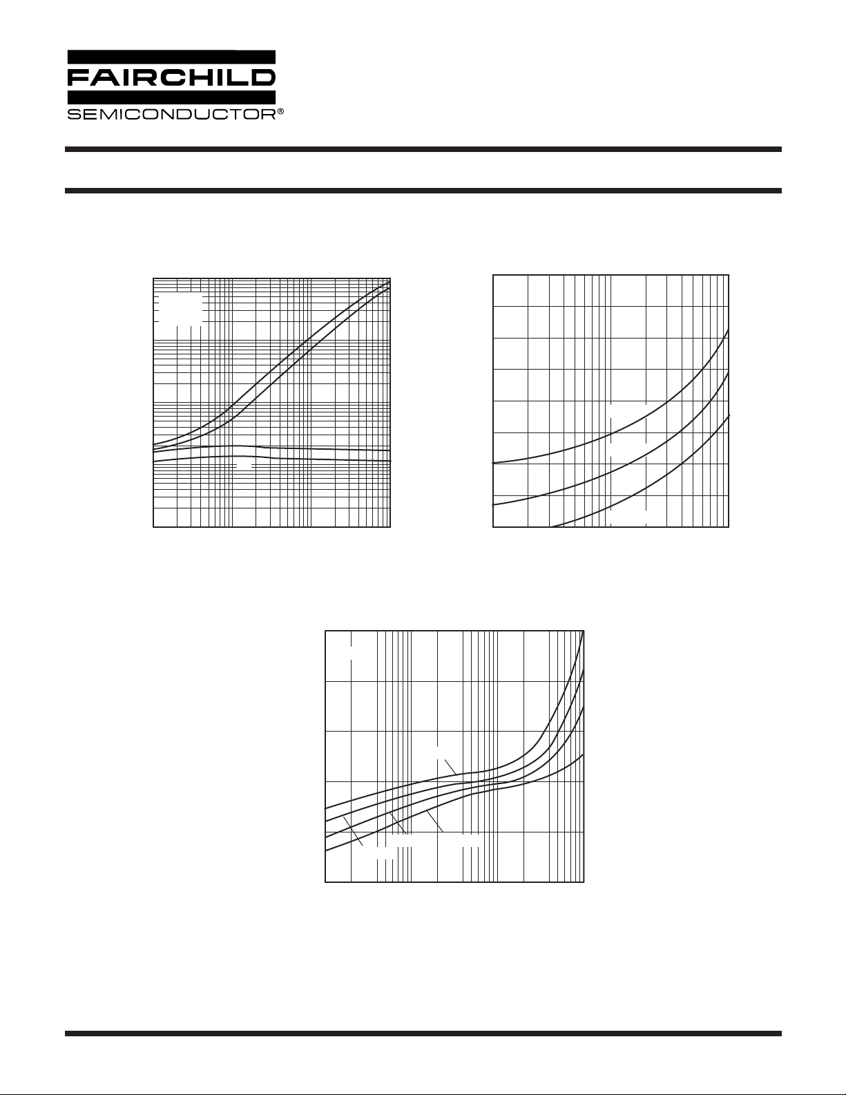
Switching Speed vs. Load Resistor
1000
IF = 10 mA
V
= 10 V
CC
= 25˚C
T
A
100
T
off
T
10
SWITCHING SPEED - (µs)
1
0.1
0.1 1 10 100
f
T
on
T
r
R-LOAD RESISTOR (kΩ)
Collector-Emitter Saturation Voltage vs Collector Current
100
TA = 25˚C
LED Forward Voltage vs. Forward Current
1.8
1.7
1.6
1.5
1.4
TA = 55˚C
1.3
- FORWARD VOLTATGE (V)
1.2
F
V
TA = 25˚C
1.1
1.0
110100
TA = 100˚C
IF - LED FORWARD CURRENT (mA)
© 2003 Fairchild Semiconductor Corporation
10
1
IF = 2.5 mA
0.1
0.01
- COLLECTOR-EMITTER SATURATION VOLTAGE (V)
CE (SAT)
0.001
V
0.01 0.1 1 10
IF = 10 mA
IF = 5 mA
I
- COLLECTOR CURRENT (mA)
C
IF = 20 mA
Page 4 of 7
7/31/03
Page 5
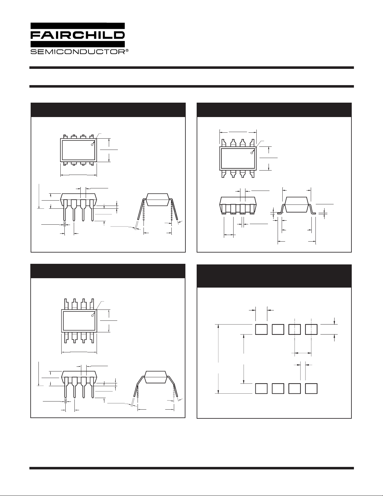
0.070 (1.78)
0.060 (1.52)
0.030 (0.76)
0.100 (2.54)
0.295 (7.49)
0.415 (10.54)
DUAL PHOTOTRANSISTOR
OPTOCOUPLERS
MCT6 MCT61 MCT62
Package Dimensions (Through Hole)
PIN 1
ID.
241
0.270 (6.86)
0.250 (6.35)
8
0.070 (1.78)
0.045 (1.14)
0.020 (0.51) MIN
0.154 (3.90)
0.120 (3.05)
0.016 (0.40)
0.008 (0.20)
15° MAX
0.300 (7.62)
TYP
0.200 (5.08)
0.140 (3.55)
SEATING PLANE
0.022 (0.56)
0.016 (0.41)
3
56 7
0.390 (9.91)
0.370 (9.40)
0.100 (2.54) TYP
Package Dimensions (0.4"Lead Spacing)
Package Dimensions (Surface Mount)
0.390 (9.91)
0.370 (9.40)
3214
567
0.100 (2.54)
Lead Coplanarity : 0.004 (0.10) MAX
TYP
0.270 (6.86)
0.250 (6.35)
8
0.070 (1.78)
0.045 (1.14)
0.022 (0.56)
0.016 (0.41)
PIN 1
ID.
0.020 (0.51)
MIN
0.300 (7.62)
TYP
0.045 [1.14]
0.315 (8.00)
MIN
0.405 (10.30)
MIN
0.016 (0.41)
0.008 (0.20)
Recommended Pad Layout for
Surface Mount Leadform
PIN 1
0.270 (6.86)
0.250 (6.35)
8
0.070 (1.78)
0.045 (1.14)
0.154 (3.90)
0.120 (3.05)
ID.
0.004 (0.10) MIN
0.016 (0.40)
0.008 (0.20)
SEATING PLANE
NOTE
0.200 (5.08)
0.140 (3.55)
0.022 (0.56)
0.016 (0.41)
3
241
56 7
0.390 (9.91)
0.370 (9.40)
0.100 (2.54) TYP
All dimensions are in inches (millimeters)
© 2003 Fairchild Semiconductor Corporation
0° to 15°
0.400 (10.16)
TYP
Page 5 of 7
7/31/03
Page 6
DUAL PHOTOTRANSISTOR
OPTOCOUPLERS
MCT6 MCT61 MCT62
ORDERING INFORMATION
Order
Option
S.S Surface Mount Lead Bend
SD .SD Surface Mount; Tape and reel
W.W 0.4” Lead Spacing
Entry
Identifier
Description
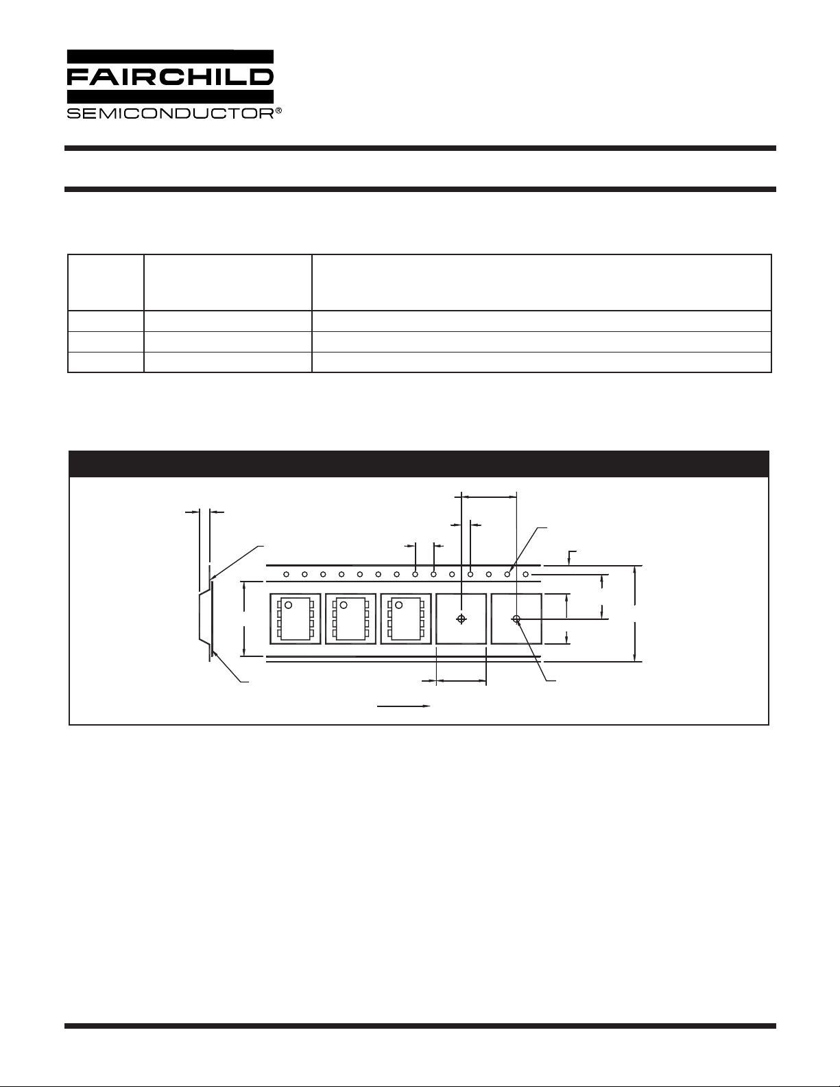
Carrier Tape Specifications
4.90 ± 0.20
0.30 ± 0.05
13.2 ± 0.2
0.1 MAX
User Direction of Feed
NOTE
All dimensions are in inches (millimeters)
4.0 ± 0.1
10.30 ± 0.20
12.0 ± 0.1
4.0 ± 0.1
Ø1.55 ± 0.05
1.75 ± 0.10
7.5 ± 0.1
16.0 ± 0.3
10.30 ± 0.20
Ø1.6 ± 0.1
© 2003 Fairchild Semiconductor Corporation
Page 6 of 7
7/31/03
Page 7

DUAL PHOTOTRANSISTOR
OPTOCOUPLERS
MCT6 MCT61 MCT62
DISCLAIMER
FAIRCHILD SEMICONDUCTOR RESERVES THE RIGHT TO MAKE CHANGES WITHOUT FURTHER NOTICE TO
ANY PRODUCTS HEREIN TO IMPROVE RELIABILITY, FUNCTION OR DESIGN. FAIRCHILD DOES NOT ASSUME
ANY LIABILITY ARISING OUT OF THE APPLICATION OR USE OF ANY PRODUCT OR CIRCUIT DESCRIBED HEREIN;
NEITHER DOES IT CONVEY ANY LICENSE UNDER ITS PATENT RIGHTS, NOR THE RIGHTS OF OTHERS.
LIFE SUPPORT POLICY
FAIRCHILD’S PRODUCTS ARE NOT AUTHORIZED FOR USE AS CRITICAL COMPONENTS IN LIFE SUPPORT DEVICES
OR SYSTEMS WITHOUT THE EXPRESS WRITTEN APPROVAL OF THE PRESIDENT OF FAIRCHILD SEMICONDUCTOR
CORPORATION. As used herein:
1. Life support devices or systems are devices or systems
which, (a) are intended for surgical implant into the body, or
(b) support or sustain life, and (c) whose failure to perform
when properly used in accordance with instructions for use
provided in the labeling, can be reasonably expected to
result in a significant injury of the user.
2. A critical component in any component of a life support
device or system whose failure to perform can be
reasonably expected to cause the failure of the life support
device or system, or to affect its safety or effectiveness.
© 2003 Fairchild Semiconductor Corporation
Page 7 of 7
7/31/03
 Loading...