

Page 1
0.048 (1.22)
0.028 (0.71)
45°
0.046 (1.16)
0.036 (0.92)
42
0.195 (4.96)
0.178 (4.52)
0.230 (5.84)
0.209 (5.31)
0.560 (14.22)
0.500 (12.70)
0.210 (5.34)
0.170 (4.32)
3
0.100 (2.54) DIA.
1
0.019 (0.48)
0.016 (0.41)
Ø4X
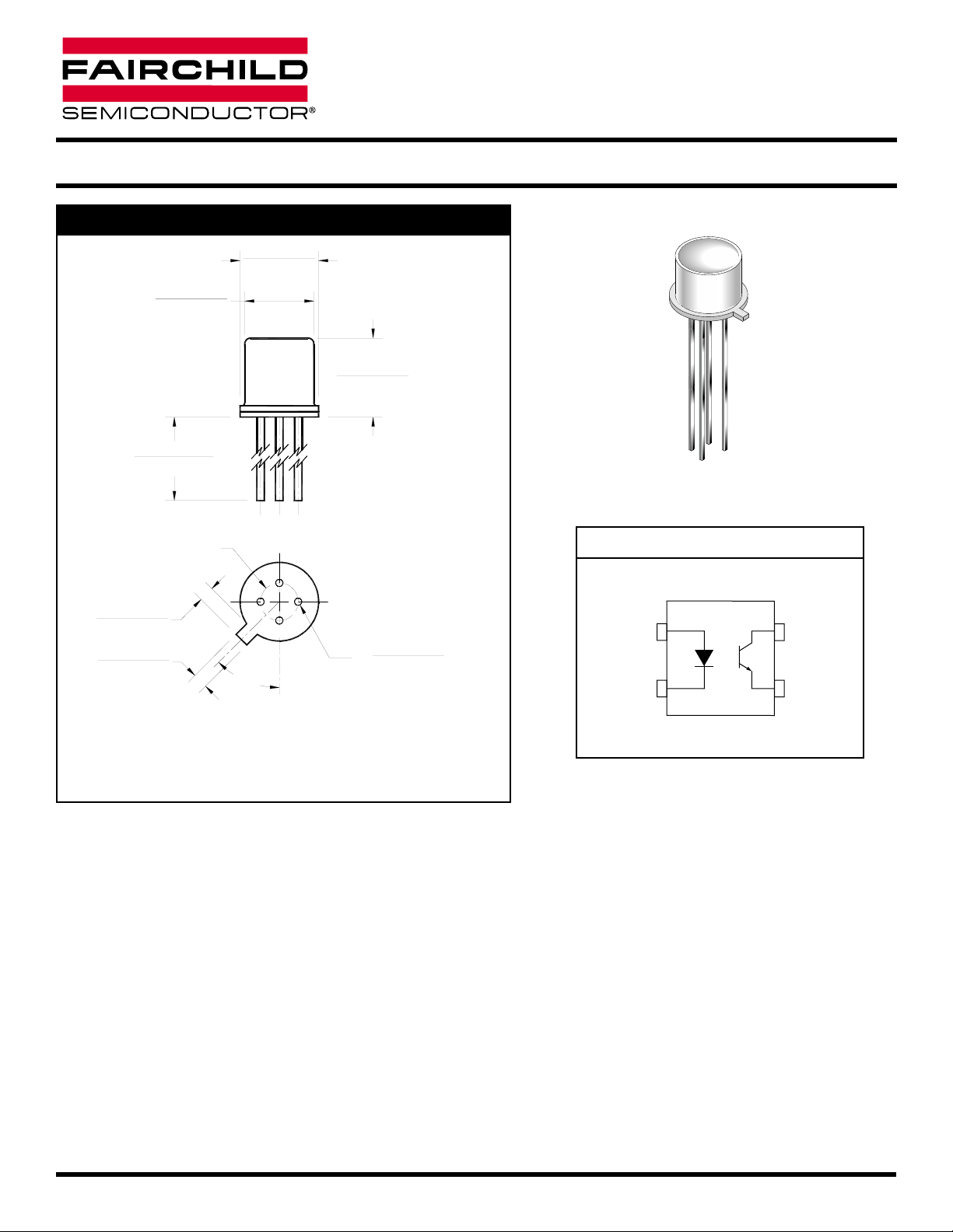
PACKAGE DIMENSIONS
FEATURES
• Hermetically package
• High current transfer ratio; typically 35%
• High isolation resistance; 10
11
ohms at 500 volts
• High voltage isolation emitter to detector
NOTES:
1. Dimensions for all drawings are in inches (mm).
2. Tolerance of ± .010 (.25) on all non-nominal dimensions
unless otherwise specified.
DESCRIPTION
The MCT4 is a standard four-lead, TO-18 package containing a GaAs infrared emitting diode optically coupled to an NPN silicon
planar phototransistor.
2001 Fairchild Semiconductor Corporation
DS300241 8/13/01 1 OF 6 www.fairchildsemi.com
SCHEMATIC
PHOTOTRANSISTOR OPTOCOUPLER
MCT4
ANODE
CATHODE
1
3
2
COLLECTOR
4 EMITTER
Page 2

www.fairchildsemi.com 2 OF 6 8/13/01 DS300241
Parameter Symbol Rating Unit
Operating Temperature
T
OPR -55 to +125 °C
Storage Temperature T
STG
-65 to +150 °C
Soldering Temperature (Flow) T
SOL-F
260 for 10 sec °C
EMITTER
P
D
Power Dissipation at 25°C Ambient
(1)
90 mW
Continuous Forward Current I
F
40 mA
Reverse Voltage V
R
3V
Forward Current - Peak (1 µs pulse, 300 pps) IF(pk) 3.0 A
DETECTOR
P
D
Power Dissipation
25°C Ambient
(2)
200 mW
Collector to Emitter Voltage
V
CEO
30 V
Emitter to Collector Voltage V
ECO
7V
COUPLER
Total Power Dissipation
(3)
P
D
250 mW
Isolation Voltage 1000 VDC
ABSOLUTE MAXIMUM RATINGS
(TA= 25°C unless otherwise specified)
ELECTRICAL / OPTICAL CHARACTERISTICS (T
A
=25°C)
PHOTOTRANSISTOR OPTOCOUPLER
MCT4
Parameters Test Conditions Symbol Min Typ Max Units
EMITTER
Forward Voltage
I
F
= 40 mA V
F
1.30 1.50 V
Reverse Current
V
R
= 3.0 V
I
R
0.15 10 µA
Capacitance
V = 0 V
C
150
pF
DETECTOR
Breakdown Voltage
Collector to Emitter
I
C
= 1.0 mA, IF= 0 BV
CEO
30 V
Emitter to Collector IE= 100 µA, IF= 0 BV
ECO
712 V
Leakage Current
Collector to Emitter
V
CE
= 10 V, IF= 0 I
CEO
550nA
Capacitance
pF
Collector to Emitter
V
CE
= 0 C
CE
2
INDIVIDUAL COMPONENT CHARACTERISTICS
NOTE:
1. Derate power linearly 1.2 mW/°C above 25°C
2. Derate power linearly 2.67 mW/°C above 25°C
3. Derate power linearly 3.3 mW/°C above 25°C
Page 3

DC Characteristics Test Conditions Symbol Min Typ Max Units
COUPLED
CTR
DC current Transfer Ratio (note 1)
VCE= 10 V , IF= 10 mA 15 35 %
Saturation Voltage
I
C
= 500 µA, IF= 10 mA
V
CE(SAT)
0.1
V
I
C
= 2 mA, IF= 50 mA
0.2 0.5
AC Characteristics Test Conditions Symbol Min Typ Max Units
Capacitance LED to Detector 1.8 pF
Bandwidth (Fig. 5)
Note 2 300 kHz
Rise Time and Fall Time (see operating schematic)
I
C
= 2 mA, VCE= 10 V , Note 3
2 µs
TRANSFER CHARACTERISTICS
(TA= 25°C Unless otherwise specified.)
PHOTOTRANSISTOR OPTOCOUPLER
MCT4
DS300241 8/13/01 3 OF 6 www.fairchildsemi.com
NOTE:
1. The current transfer ratio (IC/IF) is the ratio of the detector collector current to the LED input current with VCEat 10 volts.
2. The frequency at which i
c
is 3 dB down from the 1 kHz value.
3. Rise time (t
r
) is the time required for the collector current to increase from 10% of its final value, to 90%. Fall time (tf) is the time required
for the collector current to decrease from 90% of its initial value to 10%.
Characteristic Test Conditions Symbol Min Typ Max Units
Isolation Resistance
V
= 500 VDC
R
ISO
10
11
10
12
!
Breakdown Voltage Time = 1 sec
1000
1500
VDC
ISOLATION CHARACTERISTICS
Page 4

www.fairchildsemi.com 4 OF 6 813/01 DS300241
PHOTOTRANSISTOR OPTOCOUPLER
MCT4
Figure 1. Detector Output Characteristics
20
25
20
15
10
5
, COLLECTOR CURRENT DETECTOR (mA)
C
I
Figure 3. Dark Current vs. Temperature
-4
10
-5
10
-6
10
-7
10
-8
10
-9
DARK CURRENT (A)
10
CEO,
I
-10
10
-11
10
-12
10
IF = 60 mA
IF = 40 mA
5
10 15 20 25 30
V
, COLLECTOR VOLTAGE DETECTOR (V)
CE
V
= 10 VOLTS
CE
-40-60
-20 0 20 40 60 80 100 120 140
T
, AMBIENT TEMPERATURE (
A
IF = 20 mA
IF = 10 mA
°C)
Figure 2. Input Current vs. Output Current
20
25
V
= 10 VOLTS
20
CE
15
10
5
, COLLECTOR CURRENT DETECTOR (mA)
C
I
0
20 30 40 50 60
100
, INPUT CURRENT LED (mA)
I
F
Figure 4. Current Output vs. Temperature
110
100
90
80
70
NORMALIZED (%)
60
,
CTR
50
40
30
-40-60
T
LED CURRENT - 10 mA
V
= 10 VOLTS
CE
FREE STANDING DEVICE
-20 0 20 40 60 80 100
, AMBIENT TEMPERATURE (
A
°C)
2.0
Figure 5. Output vs. Frequency
Figure 6. Switching Time vs. Collector Current
1.8
1.6
V
= 10 VOLTS
CE
1.4
1.2
1.0
0.8
COLLECTOR CURRENT (mA)
0.6
0.4
0.2
1K 110K 100K
FREQUENCY (Hz)
L
R
R
L
= 470 Ω
= 1000 Ω
R
L
= 100 Ω
V
= 10 VOLTS
CE
12
10
= 1000 Ω
R
L
8
6
SWITCHING TIME (µs)
= 470 Ω
R
L
4
= 100 Ω
R
2
0.3 0.4 0.6 0.8 1 2 3 4 5 6 7 8 10
0.20.1
, COLLECTOR CURRENT (mA
I
C
L
)
Page 5

PHOTOTRANSISTOR OPTOCOUPLER
MCT4
DS300241 8/13/01 5 OF 6 www.fairchildsemi.com
MODULATION
INPUT
1 µF
LED
I
F
47 Ω
CONSTANT
CURRENT
INPUT
I
C
V
DETECTOR
CC
RL = 100 Ω
Figure 7. Modulation Circuit Used to Obtain Output vs.
Frequency Plot
= 10 VOLTS
OUTPUT
I
C
PULSE
INPUT
LED
47 Ω
I
F
λλ
VCC = 10 VOLTS
DETECTOR
RL = 100 Ω
Figure 8. Circuit Used to Obtain Switching Time vs.
Collector Current Plot
PULSE
OUTPUT
Page 6

DISCLAIMER
FAIRCHILD SEMICONDUCTOR RESERVES THE RIGHT TO MAKE CHANGES WITHOUT FURTHER NOTICE TO
ANY PRODUCTS HEREIN TO IMPROVE RELIABILITY, FUNCTION OR DESIGN. FAIRCHILD DOES NOT ASSUME
ANY LIABILITY ARISING OUT OF THE APPLICATION OR USE OF ANY PRODUCT OR CIRCUIT DESCRIBED
HEREIN; NEITHER DOES IT CONVEY ANY LICENSE UNDER ITS PATENT RIGHTS, NOR THE RIGHTS OF
OTHERS.
LIFE SUPPORT POLICY
FAIRCHILD’S PRODUCTS ARE NOT AUTHORIZED FOR USE AS CRITICAL COMPONENTS IN LIFE SUPPORT
DEVICES OR SYSTEMS WITHOUT THE EXPRESS WRITTEN APPROVAL OF THE PRESIDENT OF FAIRCHILD
SEMICONDUCTOR CORPORATION. As used herein:
1. Life support devices or systems are devices or
systems which, (a) are intended for surgical
implant into the body,or (b) support or sustain life,
and (c) whose failure to perform when properly
used in accordance with instructions for use provided
in labeling, can be reasonably expected to result in a
significant injury of the user.
2. A critical component in any component of a life support
device or system whose failure to perform can be
reasonably expected to cause the failure of the life
support device or system, or to affect its safety or
effectiveness.
PHOTOTRANSISTOR OPTOCOUPLER
MCT4
www.fairchildsemi.com 6 OF 6 8/13/01 DS300241
 Loading...