

Page 1
April 1999
Semiconductor
PROCESS OBSOLETE - NO NEW DESIGNS
PART WITHDRAWN
MCT3A65P100F2,
MCT3D65P100F2
65A, 1000V, P-Type
MOS-Controlled Thyristor (MCT)
[ /Title
(MCT3
A65P1
00F2,
MCT3
D65P1
00F2)
/Subject
(65A,
1000V,
PType
MOSControlled
Thyristor
(MCT)
)
/Autho
r ()
/Keywords
()
/Creator ()
/DOCI
NFO
pdfmark
Features
• 65A, -1000V
= -1.4V (Max) at I = 65A and 150oC
•V
TM
• 2000A Surge Current Capability
• 2000A/µs di/dt Capability
• MOS Insulated Gate Control
o
• 100A Gate Turn-Off Capability at 150
C
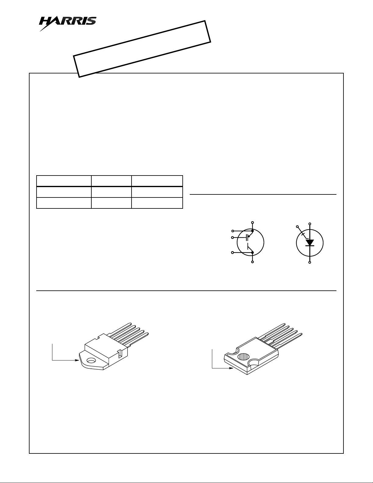
Part Number Information
PART NUMBER PACKAGE BRAND
MCT3A65P100F2 TO-247 M65P100F2
MCT3D65P100F2 MO-093AA M65P100F2
NOTE: When ordering, use the entire part number.
Packaging
JEDEC MO-093AA JEDEC STYLE TO-247
ANODE
ANODE
CATHODE
CATHODE
(FLANGE)
GATE RETURN
GATE
Description
The MCT is an MOS Controlled Thyristor designed for switching
currents on and off by negative and positive pulsed control of an
insulated MOS gate. It is designed for use in motor controls,
inverters, line switches, and other po wer s witching applications.
The MCT is especially suited for resonant (zero voltage or zero
current switching) applications. The SCR like forward drop
greatly reduces conduction power loss.
MCTs allow the control of high power circuits with very small
amounts of input energy. They feature the high peak current
capability common to SCR type thyristors, and operate at junction temperatures up to 150
Formerly developmental type TA49226.
o
C with active switching.
Symbols
(ANODE KELVIN)
GATE RETURN
GATE
CATHODE
CATHODE
(BOTTOM SIDE
METAL)
ANODE
CATHODE (TAB)
ANODE
GATE
ANODE
CATHODE
ANODE
CATHODE
GATE RETURN
GATE
[
/PageMode
/UseOutlines
/DOCVIEW
CAUTION: These devices are sensitive to electrostatic discharge. Users should follow proper ESD Handling Procedures.
Copyright
© Harris Corporation 1999
1
File Number 4454.2
Page 2
MCT3A65P100F2, MCT3D65P100F2
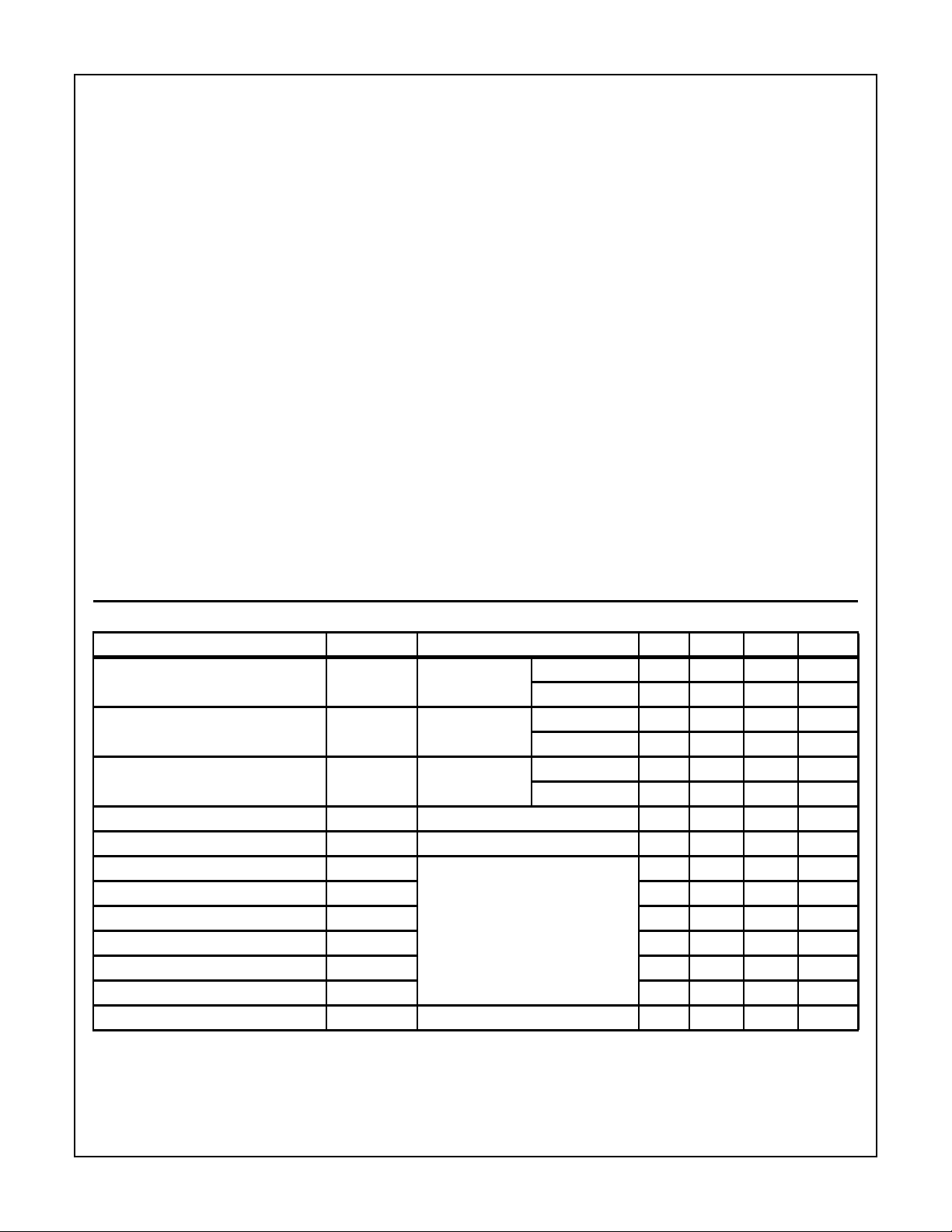
Absolute Maximum Ratings T
= 25oC, Unless Otherwise Specified
C
MCT3A65P100F2
MCT3D65P100F2 UNITS
Peak Off-State Voltage. . . . . . . . . . . . . . . . . . . . . . . . . . . . . . . . . . . . . . . . . . . . . . .V
Peak Reverse Voltage . . . . . . . . . . . . . . . . . . . . . . . . . . . . . . . . . . . . . . . . . . . . . . .V
DRM
RRM
-1000 V
5V
Continuous Cathode Current
At TC = 25oC (Package Limited). . . . . . . . . . . . . . . . . . . . . . . . . . . . . . . . . . . . . . . I
= 110oC . . . . . . . . . . . . . . . . . . . . . . . . . . . . . . . . . . . . . . . . . . . . . . . . . . . I
At T
C
Non-repetitive Peak Cathode Current (Note 1) . . . . . . . . . . . . . . . . . . . . . . . . . . . . .I
Peak Controllable Current . . . . . . . . . . . . . . . . . . . . . . . . . . . . . . . . . . . . . . . . . . . . . . I
Gate to Anode Voltage (Continuous) . . . . . . . . . . . . . . . . . . . . . . . . . . . . . . . . . . . . . V
Gate to Anode Voltage (Peak) . . . . . . . . . . . . . . . . . . . . . . . . . . . . . . . . . . . . . . . . . . V
K25
K110
KSM
KC
GA
GA
85 A
65 A
2000 A
100 A
±15 V
±20 V
Rate of Change of Voltage. . . . . . . . . . . . . . . . . . . . . . . . . . . . . . . . . . . . . . . . . . . . .dv/dt Figure 11
Rate of Change of Current . . . . . . . . . . . . . . . . . . . . . . . . . . . . . . . . . . . . . . . . . . . . . di/dt 2000 A/µs
Maximum Power Dissipation . . . . . . . . . . . . . . . . . . . . . . . . . . . . . . . . . . . . . . . . . . . . P
Power Dissipation Derating T
> 25oC . . . . . . . . . . . . . . . . . . . . . . . . . . . . . . . . . . . . . . . 2.32 W/oC
C
Operating and Storage Junction Temperature Range . . . . . . . . . . . . . . . . . . . . T
T
, T
J
STG
Maximum Temperature for Soldering
Leads at 0.063in (1.6mm) from Case for 10s . . . . . . . . . . . . . . . . . . . . . . . . . . . . . . .T
CAUTION: Stresses above those listed in “Absolute Maxim um Ratings” ma y cause permanent damage to the device . This is a stress only rating and oper ation of
the device at these or any other conditions above those indicated in the operational sections of this specification is not implied.
L
290 W
-55 to 150
300
o
C
o
C
NOTES:
1. Maximum Pulse Width of 200µs (Half Sine). Assume TJ(Initial) = 90oC and TJ(Final) = TJ(Max) = 150oC.
Electrical Specifications T
= 25oC, Unless Otherwise Specified
C
PARAMETER SYMBOL TEST CONDITIONS MIN TYP MAX UNITS
Peak Off-State Blocking Current I
Peak Reverse Blocking Current I
On-State Voltage V
Gate to Anode Leakage Current I
Input Capacitance C
Current Turn-On Delay Time t
d(ON)I
Current Rise Time t
Current Turn-Off Delay Time t
d(OFF)I
Current Fall Time t
Turn-On Energy E
Turn-Off Energy (Note 2) E
Thermal Resistance Junction To Case R
DRM
RRM
TM
GAS
ISS
rI
fI
ON
OFF
θJC
VKA= -1000V
VGA= 15V
VK= 5V
VGA= 15V
IK = I
K110
VGA = -10V
TC = 150oC--3mA
TC = 25oC - - 100 µA
TC = 150oC--4mA
TC = 25oC - - 100 µA
TC = 150oC - 1.25 1.4 V
TC = 25oC - 1.35 1.5 V
VGA = ±20V - - 200 nA
VGA = 15V, VKA = -20V, f = 1MHz - 12 - nF
TC = 150oC
L = 200µH
IK = I
K110
= 65A
VKA = -400V
- 125 - ns
-70- ns
- 770 - ns
VGA = 15V/-10V
RG = 2.2Ω
Test Circuit (Figure 13)
- 1000 1400 ns
- 2.8 - mJ
-15- mJ
- - 0.43
NOTE:
2. Turn-Off Energy Loss (E
) is defined as the integral of the instantaneous power loss starting at the trailing edge of the input pulse and
OFF
ending at the point where the cathode current equals zero (IK = 0A). All devices were tested per JEDEC Standard No. 24-1 Method for
Measurement of Power Device Turn-Off Switching Loss. This test method produces the true total Turn-Off Energy Loss. Turn-On losses
include losses due to diode recovery.
o
C/W
2
Page 3
MCT3A65P100F2, MCT3D65P100F2
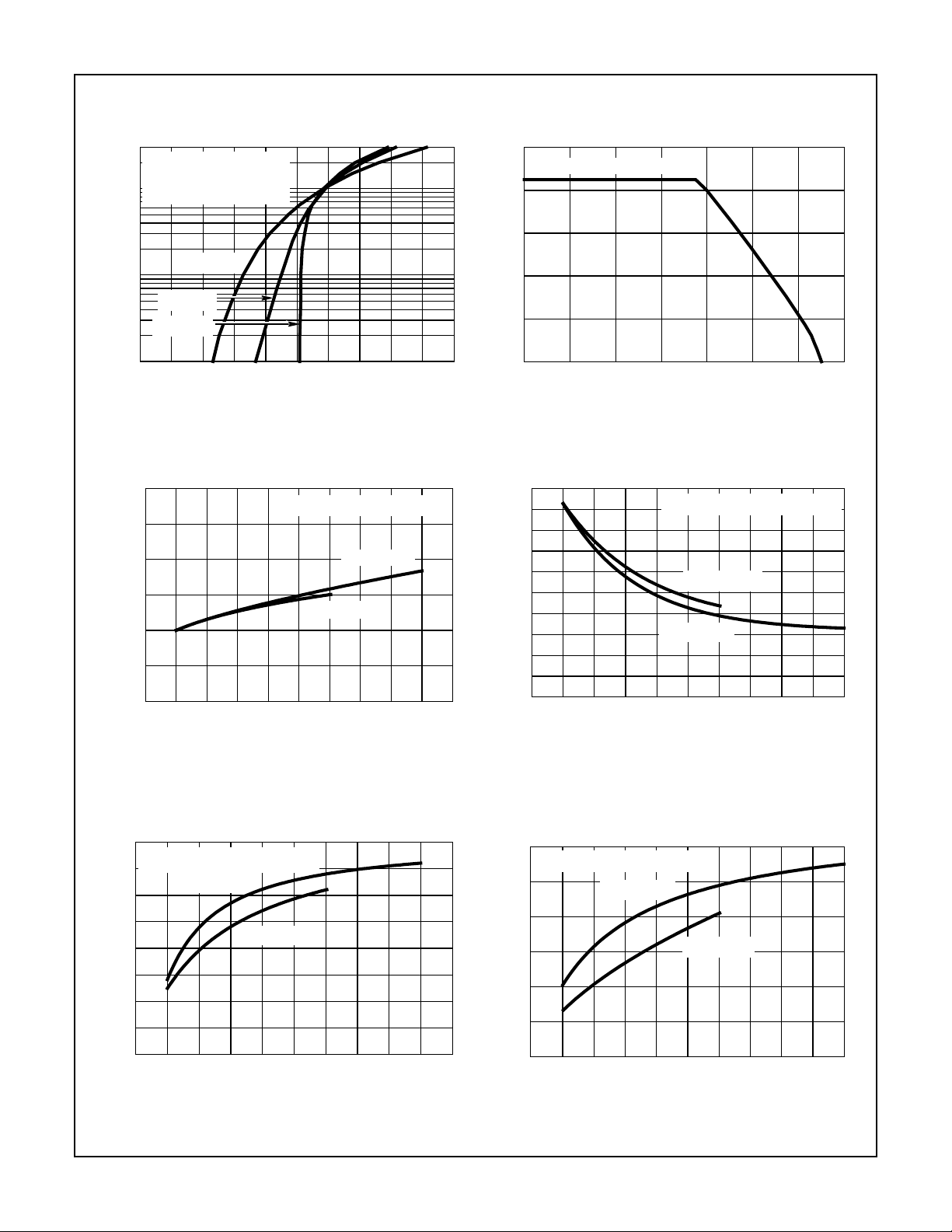
Typical Performance Curves
300
PULSE TEST
PULSE DURATION - 250µs
100
DUTY CYCLE < 2%
10
, CATHODE CURRENT (A)
K
I
1
TJ = 150oC
TJ = 25oC
TJ = -40oC
0 0.2 0.4 0.6 0.8 1.0 1.2 1.4 1.6 1.8 2.0
V
, CATHODE VOLTAGE (V)
TM
(Unless Otherwise Specified)
, DC CATHODE CURRENT (A)
K
I
100
80
60
40
20
0
20 60 80 100 120 140 160
PACKAGE LIMIT
40
T
, CASE TEMPERATURE (oC)
C
FIGURE 1. CATHODE CURRENT vs SATURATION VOLTA GE FIGURE 2. DC CATHODE CURRENT vs CASE TEMPERA TURE
180
160
140
120
100
, TURN-ON DELAY TIME (ns)
80
d(ON)I
t
60
TJ = 150oC, RG = 2.2Ω, L = 200µH
VKA = -400V
VKA = -500V
100 20304050607080 100
I
, CATHODE CURRENT (A)
K
90
2.0
1.8
1.6
1.4
1.2
1.0
0.8
0.6
, TURN-OFF DELAY TIME (µs)
0.4
0.2
d(OFF)i
t
TJ = 150oC, RG = 2.2Ω, L = 200µH
VKA = -500V
VKA = -400V
0
0
10 20 30 40 50 60 70 80 90 100
, CATHODE CURRENT (A)
I
K
FIGURE 3. TURN-ON DELAY TIME vs CATHODE CURRENT FIGURE 4. TURN-OFF DELAY TIME vs CATHODE CURRENT
80
TJ = 150oC, RG = 2.2Ω, L = 200µH
70
60
50
40
30
, RISE TIME (ns)
rI
t
20
10
0
0
VKA = -400V
10 20 30 40 50 60 70 80 90
I
, CATHODE CURRENT (A)
K
VKA = -500V
100
1.2
TJ = 150oC, RG = 2.2Ω, L = 200µH
1.0
0.8
0.6
, FALL TIME (µs)
0.4
fI
t
0.2
0
0
10 20 30 40 50 60 70 80 90 100
VKA = -400V
I
K
VKA = -500V
, CATHODE CURRENT (A)
FIGURE 5. TURN-ON RISE TIME vs CATHODE CURRENT FIGURE 6. TURN-OFF FALL TIME vs CATHODE CURRENT
3
Page 4

MCT3A65P100F2, MCT3D65P100F2
Typical Performance Curves
10
1
, TURN-ON ENERGY LOSS (mJ)
ON
E
0.4
0
10 20 30 40 50 60 70 80 90
TJ = 150oC, RG = 2.2Ω, L = 200µH
VKA = -500V
VKA = -400V
I
, CATHODE CURRENT (A)
K
(Unless Otherwise Specified) (Continued)
30
10
, TURN-OFF ENERGY LOSS (mJ)
OFF
E
1
100
0
10 20 30 40 50 60 70 80 90 100
TJ = 150oC, RG = 2.2Ω, L = 200µH
VKA = -500V
, CATHODE CURRENT (A)
I
K
VKA = -400V
FIGURE 7. TURN-ON ENERGY LOSS vs CATHODE CURRENT FIGURE 8. TURN-OFF ENERGY LOSS vs CATHODE CURRENT
100
10
TJ = 150oC,
L = 200µH
R
= 2.2Ω
G
TC = 110oC
f
= 0.05/(t
MAX1
f
= (PD - PC)/(EON + E
MAX2
P
= ALLOWABLE DISSIPATION
D
= CONDUCTION DISSIPATION
P
C
(DUTY FACTOR = 50%)
= 0.43oC/W
R
θJC
TC = 75oC
d(OFF)I
+ t
d(ON)I
OFF
)
)
120
100
TJ = 150oC, RG = 2.2Ω, L = 200µH
CS = 1.0µF
80
60
CS = 0.7µF
CS = 0µF
40
, PEAK CATHODE CURRENT (A)
20
K
I
0
0
-200
V
-400 -600
, PEAK TURN OFF VOLTAGE (V)
KA
-800
-1000
, MAX OPERATING FREQ UENCY (kHz)
MAX
1
f
10
VKA = - 400V
VKA = - 500V
, CATHODE CURRENT (A)
I
K
100
200
FIGURE 9. OPERATING FREQUENCY vs CATHODE CURRENT FIGURE 10. TURN-OFF CAPABILITY vs ANODE T O CATHODE
VOLTAGE
1100
1050
1000
950
900
, BREAKDOWN V OLTAGE (V)
DRM
850
V
800
-1
10
0
10
dv/dt, RATE OF CHANGE OF VOLTAGE (V/µs)
1
10
TJ = 150oC, VGA = 15V
2
10
3
10
FIGURE 11. BLOCKING VOLTAGE vs RATE OF CHANGE OF
VOLTAGE
4
10
100
CS = 0.1µF, TJ = 150oC
CS = 0.1µF, TJ = 25oC
CS = 1.0µF, TJ = 150oC
10
, SPIKE VOLTAGE (V)
SPIKE
V
1
0
10 20 30 40 50 60 70 80 90
di/dt, RATE OF CHANGE OF CURRENT (A/µs)
CS = 1.0µF, TJ = 25oC
CS = 2.0µF, TJ = 150oC
CS = 2.0µF, TJ = 25oC
FIGURE 12. SPIKE VOLTAGE vs RATE OF CHANGE OF
CURRENT
100
4
Page 5

MCT3A65P100F2, MCT3D65P100F2
Test Circuits and Waveforms
MAXIMUM RISE AND FALL TIME OF VG IS 200ns
G
10%
E
OFF
90%
k
10%
t
d(off)I
t
fI
E
90%
ON
t
d(on)I
t
V
200µH
G
V
K
DIODES RURG75120
I
K
DUT
V
-
+
-V
KA
I
FIGURE 13. INDUCTIVE SWITCHING TEST CIRCUIT FIGURE 14. SWITCHING TEST WAVEFORMS
V
V
G
+
G
di/dt
-
V
500Ω
-
20V
+
10kΩ
A
C
S
DUT
I
+
K
9V
4.7kΩ
-
I
K
V
AK
V
SPIKE
V
TM
rI
FIGURE 15. V
TEST CIRCUIT FIGURE 16. V
SPIKE
5
TEST WAVEFORMS
SPIKE
Page 6

MCT3A65P100F2, MCT3D65P100F2
Handling Precautions for MCTs
MOS Controlled Thyristors are susceptible to gate-insulation
damage by the electrostatic discharge of energy through the
devices. When handling these devices, care should be exercised to assure that the static charge built in the handler’s
body capacitance is not discharged through the device.
MCTs can be handled safely if the following basic precautions are taken:
1. Prior to assembly into a circuit, all leads should be kept
shorted together either by the use of metal shorting
springs or by the insertion into conductive material such
as “ECCOSORBD™ LD26” or equivalent.
2. When devices are removed by hand from their carriers,
the hand being used should be grounded by any suitable
means - for example, with a metallic wristband.
3. Tips of soldering irons should be grounded.
4. Devices should never be inserted into or removed from
circuits with power on.
5. Gate Voltage Rating - Never exceed the gate-voltage
rating of V
permanent damage to the oxide layer in the gate region.
6. Gate Termination - The gates of these devices are
essentially capacitors. Circuits that leave the gate opencircuited or floating should be avoided. These conditions
can result in turn-on of the device due to voltage buildup
on the input capacitor due to leakage currents or pickup.
7. Gate Protection - These devices do not have an internal
monolithic zener diode from gate to anode. If gate
protection is required an external zener is recommended.
. Exceeding the rated VGA can result in
GAM
Operating Frequency Information
Operating frequency information for a typical device (Figure
9) is presented as a guide for estimating device performance
for a specific application. Other typical frequency vs cathode
current (I
for a typical unit in Figures 3 to 8. The operating frequency
plot (Figure 9) of a typical device shows f
whichever is smaller at each point. The information is based
on measurements of a typical device and is bounded by the
maximum rated junction temperature.
f
MAX1
time (the denominator) has been arbitrarily held to 10% of
the on- state time for a 50% duty factor. Other definitions are
possible. t
Device turn-off delay can establish an additional frequency
limiting condition for an application other than T
t
d(OFF)
lightly loaded condition.
f
MAX2
able dissipation (P
sum of device switching and conduction losses must not exceed
P
. A 50% duty factor was used (Figure 9) and the conduction
D
losses (P
E
ON
in Figure 14. E
loss (I
instantaneous power loss (I
losses are included in the calculation for E
ode current equals zero (I
) plots are possible using the information shown
AK
or f
MAX1
is defined by f
and t
d(OFF)I
MAX1
= 0.05/(t
d(ON)I
d(OFF)I
are defined in Figure 14.
+ t
d(ON)I
). Dead-
is important when controlling output ripple under a
is defined by f
) are approximated by PC = (VAK x IAK)/2.
C
and E
AK
are defined in the switching wav eforms shown
OFF
ON
x VAK) during turn-on and E
= (PD - PC)/(E
MAX2
) is defined by PD=(T
D
+ EON). The allow-
OFF
JMAX-TC
)/R
θJC
is the integral of the instantaneous power
is the integral of the
OFF
x VAK) during turn-off. All tail
= 0).
K
AK
; i.e. the cath-
OFF
MAX2
JMAX
. The
.
ECCOSORBD is a Trademark of Emerson and Cumming, Inc.
6
Page 7

MCT3A65P100F2, MCT3D65P100F2
TO-247
5 LEAD JEDEC STYLE TO-247 PLASTIC PACKAGE
E
Q
ØR
D
A
ØS
TERM. 6
ØP
SYMBOL
INCHES MILLIMETERS
NOTESMIN MAX MIN MAX
A 0.180 0.190 4.58 4.82 -
b 0.046 0.051 1.17 1.29 2, 3
b
1
b
2
0.060 0.070 1.53 1.77 1, 2
0.095 0.105 2.42 2.66 1, 2
c 0.020 0.026 0.51 0.66 1, 2, 3
L
1
L
123
e
1
b
1
b
2
c
b
45
e
LEAD 1 - GATE
LEAD 2 - GATE RETURN
LEAD 3 - CATHODE
LEAD 4 - ANODE
LEAD 5 ANODE
TERM. 6 CATHODE
J
1
12345
BACK VIEW
D 0.800 0.820 20.32 20.82 E 0.605 0.625 15.37 15.87 -
e 0.110 TYP 2.79 TYP 4
e
1
J
1
0.438 BSC 11.12 BSC 4
0.090 0.105 2.29 2.66 5
L 0.620 0.640 15.75 16.25 -
L
1
0.145 0.155 3.69 3.93 1
ØP 0.138 0.144 3.51 3.65 -
Q 0.210 0.220 5.34 5.58 ØR 0.195 0.205 4.96 5.20 ØS 0.260 0.270 6.61 6.85 -
NOTES:
1. Lead dimension and finish uncontrolled in L1.
2. Lead dimension (without solder).
3. Add typically 0.002 inches (0.05mm) for solder coating.
4. Position of lead to be measured 0.250 inches (6.35mm) from bottom
of dimension D.
5. Position of lead to be measured 0.100 inches (2.54mm) from bottom
of dimension D.
6. Controlling dimension: Inch.
7. Revision 1 dated 1-93.
7
Page 8

MCT3A65P100F2, MCT3D65P100F2
MO-093AA
5 LEAD JEDEC MO-093AA PLASTIC PACKAGE
E
ØP
A
A
1
SYMBOL
INCHES MILLIMETERS
NOTESMIN MAX MIN MAX
A 0.185 0.195 4.70 4.95 -
Q
H
1
A
1
0.058 0.062 1.48 1.57 -
b 0.049 0.053 1.25 1.34 3, 4, 5
D
TERM. 6
b
1
0.070 0.080 1.78 2.03 3, 4
c 0.018 0.022 0.46 0.55 3, 4, 5
D 0.800 0.820 20.32 20.82 E 0.615 0.625 15.63 15.87 2
L
1
L
o
75
1234 5
e
e
1
LEAD 1 - GATE
LEAD 2 - GATE RETURN
LEAD 3 - CATHODE
LEAD 4 - ANODE
LEAD 5 ANODE
TERM. 6 CATHODE
b
1
c
e 0.110 TYP 2.80 TYP 7
e
1
H
1
J
1
0.438 BSC 11.12 BSC 7
- 0.330 - 8.38 -
0.115 0.125 2.93 3.17 8
L 0.575 0.600 14.61 15.24 -
b
J
1
L
1
- 0.130 - 3.30 3
ØP 0.159 0.163 4.04 4.14 -
Q 0.176 0.186 4.48 4.72 2
NOTES:
1. These dimensions are within allowable dimensions of Rev. A of
JEDEC MO-093AA outline dated 2-90.
2. Tab outline optional within boundaries of dimensions E and Q.
3. Lead dimension and finish uncontrolled in L1.
4. Lead dimension (without solder).
5. Add typically 0.002 inches (0.05mm) for solder coating.
6. Maximum radius of 0.050 inches (1.27mm) on all body edges and
corners.
7. Position of lead to be measured 0.250 inches (6.35mm) from bottom
of dimension D.
8. Position of lead to be measured 0.100 inches (2.54mm) from bottom
of dimension D.
9. Controlling dimension: Inch.
10. Revision 1 dated 1-93.
8
 Loading...