

Page 1

MCP1700
1
3
2
V
IN
GND V
OUT
MCP1700
1
2
3
V
IN
GND V
OUT
MCP1700
3-Pin SOT-23 3-Pin SOT-89
321
GND V
INVOUT
MCP1700
3-Pin TO-92
V
IN
Low Quiescent Current LDO
Features
• 1.6 µA Typical Quiescent Current
• Input Operating Voltage Range: 2.3V to 6.0V
• Output Voltage Range: 1.2V to 5.0V
• 250 mA Output Current for output voltages ≥ 2.5V
• 200 mA Output Current for output voltages < 2.5V
• Low Dropout (LDO) voltage
- 178 mV typical @ 250 mA for V
• 0.4% Typical Output Voltage Tolerance
• Standard Output Voltage Options:
- 1.2V, 1.8V, 2.5V, 3.0V, 3.3V, 5.0V
• Stable with 1.0 µF Ceramic Output capacitor
• Short Circuit Protection
• Overtemperature Protection
OUT
= 2.8V
Applications
• Battery-powered Devices
• Battery-powered Alarm Circuits
• Smoke Detectors
2
Detectors
•CO
• Pagers and Cellular Phones
• Smart Battery Packs
• Low Quiescent Current Voltage Reference
•PDAs
• Digital Cameras
• Microcontroller Power
General Description
The MCP1700 is a family of CMOS low dropout (LDO)
voltage regulators that can deliver up to 250 mA of
current while consuming only 1.6 µA of quiescent
current (typical). The input operating range is specified
from 2.3V to 6.0V, making it an ideal choice for two and
three primary cell battery-powered applications, as well
as single cell Li-Ion-powered applications.
The MCP1700 is capable of delivering 250 mA with
only 178 mV of input to output voltage differential
= 2.8V). The output voltage tolerance of the
(V
OUT
MCP1700 is typically ±0.4% at +25°C and ±3%
maximum over the operating junction temperature
range of -40°C to +125°C.
Output voltages available for the MCP1700 range from
1.2V to 5.0V. The LDO output is stable when using only
1 µF output capacitance. Ceramic, tantalum or
aluminum electrolytic capacitors can all be used for
input and output. Overcurrent limit and overtemperature
shutdown provide a robust solution for any application.
Package options include the SOT-23, SOT-89 and
TO-92.
Package Types
Related Literature
• AN765, “Using Microchip’s Micropower LDOs”,
DS00765, Microchip Technology Inc., 2002
• AN766, “Pin-Compatible CMOS Upgrades to
BiPolar LDOs”, DS00766,
Microchip Technology Inc., 2002
• AN792, “A Method to Determine How Much
Power a SOT23 Can Dissipate in an Application”,
DS00792, Microchip Technology Inc., 2001
© 2007 Microchip Technology Inc. DS21826B-page 1
Page 2

MCP1700
+
-
MCP1700
V
IN
V
OUT
GND
+V
IN
Error Amplifier
Voltage
Reference
Over Current
Over Temperature
MCP1700
GND
V
OUT
V
IN
C
IN
1 µF Ceramic
C
OUT
1 µF Ceramic
V
OUT
V
IN
(2.3V to 3.2V)
1.8V
I
OUT
150 mA
Functional Block Diagrams
Typical Application Circuits
DS21826B-page 2 © 2007 Microchip Technology Inc.
Page 3

MCP1700
1.0 ELECTRICAL
CHARACTERISTICS
† Notice: Stresses above those listed under “Maximum
Ratings” may cause permanent damage to the device. This is
a stress rating only and functional operation of the device at
those or any other conditions above those indicated in the
Absolute Maximum Ratings †
V
............................................................................................+6.5V
DD
All inputs and outputs w.r.t. .............(V
Peak Output Current ....................................Internally Limited
-0.3V) to (VIN+0.3V)
SS
operational listings of this specification is not implied.
Exposure to maximum rating conditions for extended periods
may affect device reliability.
Storage temperature .....................................-65°C to +150°C
Maximum Junction Temperature................................... 150°C
Operating Junction Temperature...................-40°C to +125°C
ESD protection on all pins (HBM;MM)............... ≥ 4kV; ≥ 400V
DC CHARACTERISTICS
Electrical Characteristics: Unless otherwise specified, all limits are established for VIN=VR+1, I
C
=1µF (X7R), CIN=1µF(X7R), TA= +25°C.
OUT
Boldface type applies for junction temperatures, T
(Note 6) of -40°C to +125°C.
J
Parameters Sym Min Typ Max Units Conditions
Input / Output Characteristics
Input Operating Voltage V
Input Quiescent Current I
Maximum Output Current I
Output Short Circuit Current I
OUT_mA
OUT_SC
IN
q
2.3 — 6.0 V Note 1
—1.6 4 µA IL=0mA, VIN=VR +1V
250
200
—
—
—
—
mA For VR≥ 2.5V
For V
— 408 — mA VIN=VR+V, V
Current (peak current) measured
10 ms after short is applied.
Output Voltage Regulation V
Temperature Coefficient TCV
V
OUT
Line Regulation ΔV
(V
OUT
Load Regulation ΔV
Dropout Voltage
V
> 2.5V
R
Dropout Voltage
V
< 2.5V
R
OUT/VOUT
V
IN-VOUT
V
IN-VOUT
Output Rise Time T
Output Noise e
Note 1: The minimum V
2: V
is the nominal regulator output voltage. For example: VR= 1.2V, 1.5V, 1.8V, 2.5V, 2.8V, 3.0V, 3.3V, 4.0V, 5.0V. The
R
input voltage (V
3: TCV
OUT
= (V
temperature range. V
must meet two conditions: VIN≥ 2.3V and VIN ≥ (VR + 3.0%) +V
IN
+ 1.0V); I
IN=VR
OUT-HIGH-VOUT-LOW
OUT-LOW
OUT
OUT
OUT
XΔVIN)
R
N
VR-3.0%
V
-2.0%
R
±0.4%VR+3.0%
V
R
V
+2.0%
R
V Note 2
— 50 — ppm/°C Note 3
/
-1.0 ±0.75 +1.0 %/V (V
R
-1.5 ±1.0 +1.5 %IL= 0.1 mA to 250 mA for VR≥ 2.5V
I
= 0.1 mA to 200 mA for VR< 2.5V
L
Note 4
— 178 350 mV IL= 250 mA, (Note 1, Note 5)
— 150 350 mV IL= 200 mA, (Note 1, Note 5)
— 500 — µs 10% VR to 90% VR VIN= 0V to 6V,
R
L
—3—µV/(Hz)
= 100 µA.
OUT
) *106 / (VR* ΔTemperature), V
OUT-HIGH
1/2
IL= 100 mA, f = 1 kHz, C
DROPOUT
= highest voltage measured over the
= lowest voltage measured over the temperature range.
4: Load regulation is measured at a constant junction temperature using low duty cycle pulse testing. Changes in output
voltage due to heating effects are determined using thermal regulation specification TCV
5: Dropout voltage is defined as the input to output differential at which the output voltage drops 2% below its measured
value with a V
+ 1V differential applied.
R
6: The maximum allowable power dissipation is a function of ambient temperature, the maximum allowable junction
temperature and the thermal resistance from junction to air (i.e., T
dissipation will cause the device operating junction temperature to exceed the maximum 150°C rating. Sustained
, TJ, θJA). Exceeding the maximum allowable power
A
junction temperatures above 150°C can impact the device reliability.
7: The junction temperature is approximated by soaking the device under test at an ambient temperature equal to the
desired Junction temperature. The test time is small enough such that the rise in the Junction temperature over the
ambient temperature is not significant.
= 100 µA,
LOAD
< 2.5V
R
OUT
+1)V ≤ VIN ≤ 6V
=50Ω resistive
.
.
OUT
=GND,
OUT
=1µF
© 2007 Microchip Technology Inc. DS21826B-page 3
Page 4

MCP1700
DC CHARACTERISTICS (CONTINUED)
Electrical Characteristics: Unless otherwise specified, all limits are established for VIN=VR+1, I
C
=1µF (X7R), CIN=1µF(X7R), TA= +25°C.
OUT
Boldface type applies for junction temperatures, T
(Note 6) of -40°C to +125°C.
J
Parameters Sym Min Typ Max Units Conditions
Power Supply Ripple
Rejection Ratio
Thermal Shutdown Protection T
Note 1: The minimum V
2: V
is the nominal regulator output voltage. For example: VR= 1.2V, 1.5V, 1.8V, 2.5V, 2.8V, 3.0V, 3.3V, 4.0V, 5.0V. The
R
input voltage (V
3: TCV
temperature range. V
OUT
= (V
OUT-HIGH-VOUT-LOW
PSRR — 44 — dB f = 100 Hz, C
SD
must meet two conditions: VIN≥ 2.3V and VIN ≥ (VR + 3.0%) +V
IN
+ 1.0V); I
IN=VR
= lowest voltage measured over the temperature range.
OUT-LOW
— 140 — °C VIN=VR+1, IL= 100 µA
= 100 µA.
OUT
) *106 / (VR* ΔTemperature), V
OUT-HIGH
= highest voltage measured over the
V
INAC
V
R
DROPOUT
4: Load regulation is measured at a constant junction temperature using low duty cycle pulse testing. Changes in output
voltage due to heating effects are determined using thermal regulation specification TCV
5: Dropout voltage is defined as the input to output differential at which the output voltage drops 2% below its measured
value with a V
+ 1V differential applied.
R
6: The maximum allowable power dissipation is a function of ambient temperature, the maximum allowable junction
temperature and the thermal resistance from junction to air (i.e., T
, TJ, θJA). Exceeding the maximum allowable power
A
dissipation will cause the device operating junction temperature to exceed the maximum 150°C rating. Sustained
junction temperatures above 150°C can impact the device reliability.
7: The junction temperature is approximated by soaking the device under test at an ambient temperature equal to the
desired Junction temperature. The test time is small enough such that the rise in the Junction temperature over the
ambient temperature is not significant.
= 100 µA,
LOAD
=1µF, IL=50mA,
OUT
=100mVpk-pk, CIN=0µF,
=1.2V
.
.
OUT
TEMPERATURE SPECIFICATIONS
Electrical Characteristics: Unless otherwise specified, all limits are established for V
C
= 1 µF (X7R), CIN=1µF (X7R), TA= +25°C.
OUT
Boldface type applies for junction temperatures, T
(Note 1) of -40°C to +125°C.
J
Parameters Sym Min Typ Max Units Conditions
Temperature Ranges
Specified Temperature Range T
Operating Temperature Range T
Storage Temperature Range T
A
A
A
-40 +125 °C
-40 +125 °C
-65 +150 °C
Thermal Package Resistance
Thermal Resistance, SOT-23
θ
JA
—336—°C/W
— 230 — °C/W Typical FR4 4-layer Application
Thermal Resistance, SOT-89 θ
Thermal Resistance, TO-92
JA
θ
JA
— 52 — °C/W Typical, 1 square inch of copper
— 131.9 — °C/W
Note 1: The maximum allowable power dissipation is a function of ambient temperature, the maximum allowable junction
temperature and the thermal resistance from junction to air (i.e., T
dissipation will cause the device operating junction temperature to exceed the maximum 150°C rating. Sustained
, TJ, θJA). Exceeding the maximum allowable power
A
junction temperatures above 150°C can impact the device reliability.
IN=VR
+1, I
LOAD
= 100 µA,
Minimum Trace Width Single Layer
Board
EIA/JEDEC JESD51-751-7
4-Layer Board
DS21826B-page 4 © 2007 Microchip Technology Inc.
Page 5

MCP1700
1.0
1.2
1.4
1.6
1.8
2.0
2.2
2.4
2.6
2.8
3.0
2.0 2.5 3.0 3.5 4.0 4.5 5.0 5.5 6.0
Input Voltage (V)
Quiescent Current (µA)
TJ = - 40°C
TJ = +25°C
TJ = +125°C
VR = 1.2V
I
OUT
= 0 µA
0
5
10
15
20
25
30
35
40
45
50
0 25 50 75 100 125 150 175 200 225 250
Load Current (mA)
Ground Current (µA)
V
R
V
TJ = - 40°C
TJ = +25°C
TJ = +125°C
1.25
1.50
1.75
2.00
2.25
2.50
-40 -25 -10 5 20 35 50 65 80 95 110 125
Junction Temperature (°C)
Quiscent Current (µA)
VR = 5.0V
VR = 2.8V
VR = 1.2V
VIN = VR + 1V
I
OUT
= 0 µA
1.190
1.192
1.194
1.196
1.198
1.200
1.202
1.204
1.206
2 2.5 3 3.5 4 4.5 5 5.5 6
Input Voltage (V)
Output Voltage (V)
TJ = - 40°C
TJ = +25°C
TJ = +125°C
VR = 1.2V
I
OUT
= 0.1 mA
1.77
1.775
1.78
1.785
1.79
1.795
1.8
2 2.5 3 3.5 4 4.5 5 5.5 6
Input Voltage (V)
Output Voltage (V)
TJ = - 40°C
TJ = +25°C
TJ = +125°C
VR = 1.8V
I
OUT
= 0.1 mA
2.778
2.780
2.782
2.784
2.786
2.788
2.790
2.792
2.794
2.796
2.798
2.800
3.3 3.6 3.9 4.2 4.5 4.8 5.1 5.4 5.7 6
Input Voltage (V)
Output Voltage (V)
TJ = - 40°C
TJ = +25°C
TJ = +125°C
VR = 2.8V
I
OUT
= 0.1 mA
2.0 TYPICAL PERFORMANCE CURVES
Note: The graphs and tables provided following this note are a statistical summary based on a limited number of
samples and are provided for informational purposes only. The performance characteristics listed herein
are not tested or guaranteed. In some graphs or tables, the data presented may be outside the specified
operating range (e.g., outside specified power supply range) and therefore outside the warranted range.
Note: Unless otherwise indicated: VR= 1.8V, C
= 1 µF Ceramic (X7R), CIN= 1 µF Ceramic (X7R), IL= 100 µA,
OUT
TA= +25°C, VIN=VR+V.
Note: Junction Temperature (TJ) is approximated by soaking the device under test to an ambient temperature equal to the desired junction
temperature. The test time is small enough such that the rise in Junction temperature over the Ambient temperature is not significant.
FIGURE 2-1: Input Quiescent Current vs. Input Voltage.
= 2.8
FIGURE 2-4: Output Voltage vs. Input
Voltage (V
=1.2V).
R
FIGURE 2-2: Ground Current vs. Load Current.
FIGURE 2-3: Quiescent Current vs. Junction Temperature.
© 2007 Microchip Technology Inc. DS21826B-page 5
FIGURE 2-5: Output Voltage vs. Input
Voltage (V
=1.8V).
R
FIGURE 2-6: Output Voltage vs. Input
Voltage (V
=2.8V).
R
Page 6

MCP1700
4.955
4.960
4.965
4.970
4.975
4.980
4.985
4.990
4.995
5.000
5 5.2 5.4 5.6 5.8 6
Input Voltage (V)
Output Voltage (V)
TJ = - 40°C
TJ = +25°C
TJ = +125°C
VR = 5.0V
I
OUT
= 0.1 mA
1.15
1.16
1.17
1.18
1.19
1.20
1.21
0 25 50 75 100 125 150 175 200
Load Curent (mA)
Output Voltage (V)
TJ = - 40°C
TJ = +25°C
TJ = +125°C
VR = 1.2V
V
IN
= VR + 1V
1.778
1.780
1.782
1.784
1.786
1.788
1.790
1.792
0 25 50 75 100 125 150 175 200
Load Current (mA)
Output Voltage (V)
TJ = - 40°C
TJ = +25°C
TJ = +125°C
VR = 1.8V
V
IN
= VR + 1V
2.778
2.780
2.782
2.784
2.786
2.788
2.790
2.792
2.794
2.796
2.798
0 50 100 150 200 250
Load Current (mA)
Output Voltage (V)
TJ = - 40°C
TJ = +25°C
TJ = +125°C
VR = 2.8V
V
IN
= VR + 1V
4.955
4.960
4.965
4.970
4.975
4.980
4.985
4.990
4.995
5.000
0 50 100 150 200 250
Load Current (mA)
Output Voltage (V)
TJ = - 40°C
TJ = +25°C
TJ = +125°C
VR = 5.0V
V
IN
= VR + 1V
0
0.05
0.1
0.15
0.2
0.25
0 25 50 75 100 125 150 175 2 00 225 25 0
Load Current (mA)
Dropout Votage (V)
TJ = - 40°C
TJ = +25°C
TJ = +125°C
V
R
Note: Unless otherwise indicated: VR= 1.8V, C
OUT
TA= +25°C, VIN=VR+1V.
FIGURE 2-7: Output Voltage vs. Input
Voltage (V
=5.0V).
R
= 1 µF Ceramic (X7R), CIN= 1 µF Ceramic (X7R), IL= 100 µA,
FIGURE 2-10: Output Voltage vs. Load
Current (V
=2.8V).
R
FIGURE 2-8: Output Voltage vs. Load
Current (V
=1.2V).
R
FIGURE 2-9: Output Voltage vs. Load
Current (V
DS21826B-page 6 © 2007 Microchip Technology Inc.
R
=1.8V).
FIGURE 2-11: Output Voltage vs. Load
Current (V
=5.0V).
R
= 2.8V
FIGURE 2-12: Dropout Voltage vs. Load
Current (V
=2.8V).
R
Page 7

MCP1700
0
0.02
0.04
0.06
0.08
0.1
0.12
0.14
0.16
0 25 50 75 100 125 150 175 200 225 250
Load Current (mA)
Dropout Voltage (V)
TJ = - 40°C
TJ = +25°C
TJ = +125°C
V
R
0.01
0.1
1
10
0.01 0.1 1 10 100 1000
Frequency (KHz)
Noise (µV/
√
Hz)
VIN = 2.5V
V
R
= 1.2V
I
OUT
= 50ma
VIN = 2.8V
V
R
= 1.8V
I
OUT
= 50ma
VIN = 3.8V
V
R
= 2.8V
I
OUT
= 50ma
Note: Unless otherwise indicated: VR= 1.8V, C
OUT
TA = +25°C, VIN=VR+1V.
= 5.0V
FIGURE 2-13: Dropout Voltage vs. Load
Current (V
=5.0V).
R
= 1 µF Ceramic (X7R), CIN = 1 µF Ceramic (X7R), IL= 100 µA,
FIGURE 2-16: Noise vs. Frequency.
FIGURE 2-14: Power Supply Ripple
Rejection vs. Frequency (V
FIGURE 2-15: Power Supply Ripple
Rejection vs. Frequency (V
© 2007 Microchip Technology Inc. DS21826B-page 7
=1.2V).
R
=2.8V).
R
FIGURE 2-17: Dynamic Load Step
(V
=1.2V).
R
FIGURE 2-18: Dynamic Load Step
(V
=1.8V).
R
Page 8

MCP1700
Note: Unless otherwise indicated: VR= 1.8V, C
TA= +25°C, VIN=VR+1V.
FIGURE 2-19: Dynamic Load Step
(V
=2.8V).
R
= 1 µF Ceramic (X7R), CIN= µF Ceramic (X7R), IL= 100 µA,
OUT
FIGURE 2-22: Dynamic Load Step
(V
=5.0V).
R
FIGURE 2-20: Dynamic Load Step
(V
=1.8V).
R
FIGURE 2-21: Dynamic Load Step
(V
=2.8V).
R
FIGURE 2-23: Dynamic Line Step
(V
=2.8V).
R
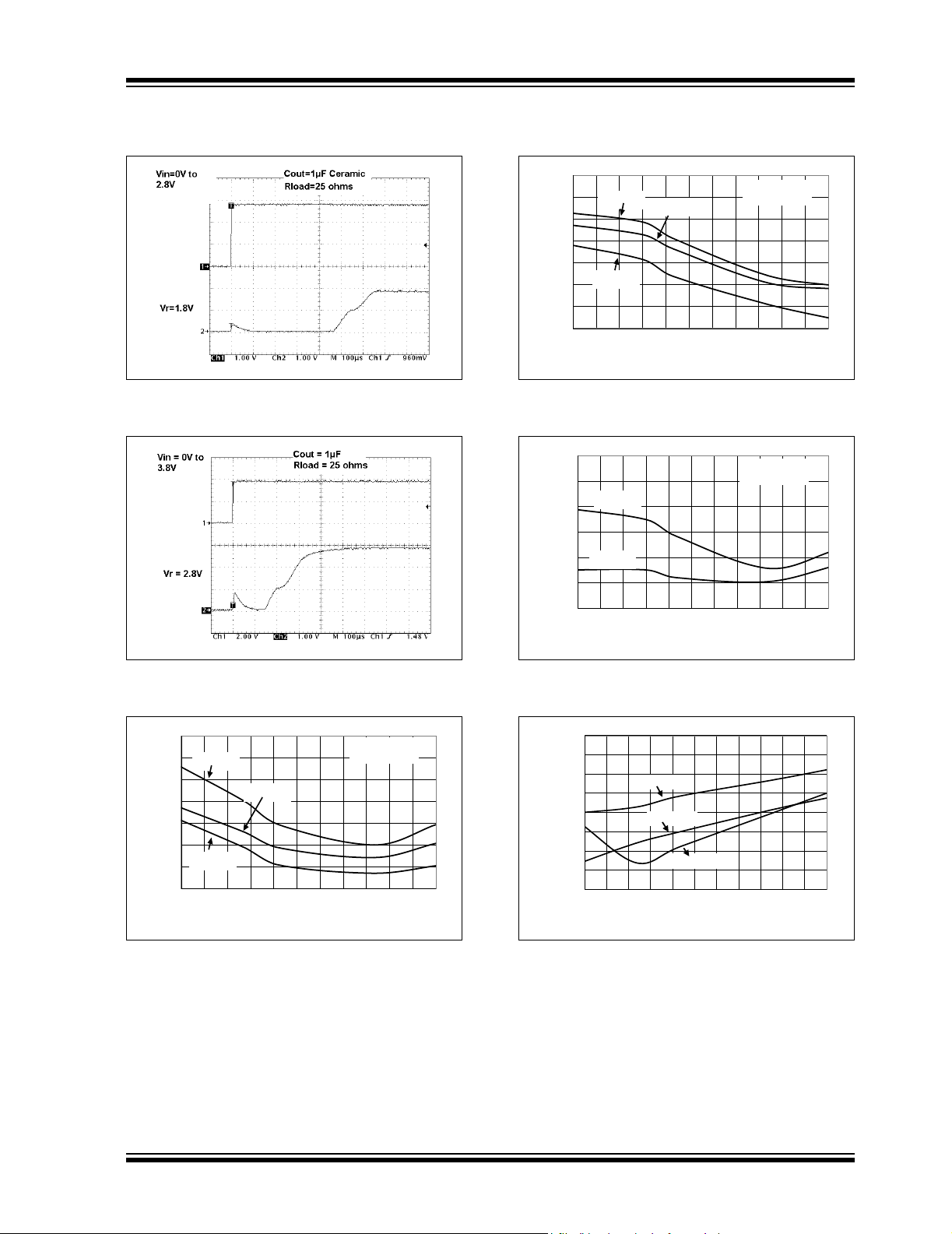
FIGURE 2-24: Startup From VIN
(V
=1.2V).
R
DS21826B-page 8 © 2007 Microchip Technology Inc.
Page 9
MCP1700
-0.4
-0.3
-0.2
-0.1
0
0.1
0.2
0.3
-40 -25 -10 5 20 35 50 65 80 95 110 125
Junction Temperature (°C)
Load Regulation (%)
VR = 1.8V
I
OUT
= 0 to 200 mA
V
IN
= 2.2V
V
IN
= 5.0V
V
IN
= 3.5V
-0.7
-0.6
-0.5
-0.4
-0.3
-0.2
-0.1
0
-40 -25 -10 5 20 35 50 65 80 95 110 125
Junction Temperature (°C)
Load Regulation (%)
VR = 2.8V
I
OUT
= 0 to 250 mA
V
IN
= 5.0V
V
IN
= 4.3V
V
IN
= 3.3V
-0.2
-0.15
-0.1
-0.05
0
0.05
0.1
-40 -25 -10 5 20 35 50 65 80 95 110 125
Junction Temperature (°C)
Load Regulation (%)
VR = 5.0V
I
OUT
= 0 to 250 mA
V
IN
= 5.5V
V
IN
= 6.0V
-0.3
-0.25
-0.2
-0.15
-0.1
-0.05
0
0.05
0.1
-40 -25 -10 5 20 35 50 65 80 95 110 125
Junction Temperature (°C)
Line Regulation (%/V)
VR = 1.8V
VR = 1.2V
VR = 2.8V
Note: Unless otherwise indicated: VR= 1.8V, C
TA= +25°C, VIN=VR+1V.
FIGURE 2-25: Start-up From VIN
(V
=1.8V).
R
= 1 µF Ceramic (X7R), CIN= 1 µF Ceramic (X7R), IL= 100 µA,
OUT
FIGURE 2-28: Load Regulation vs.
Junction Temperature (V
=2.8V).
R
FIGURE 2-26: Start-up From V
(V
=2.8V).
R
FIGURE 2-27: Load Regulation vs.
Junction Temperature (V
© 2007 Microchip Technology Inc. DS21826B-page 9
=1.8V).
R
IN
FIGURE 2-29: Load Regulation vs.
Junction Temperature (V
=5.0V).
R
FIGURE 2-30: Line Regulation vs.
Temperature (V
= 1.2V, 1.8V, 2.8V).
R
Page 10
MCP1700
3.0 PIN DESCRIPTIONS
The descriptions of the pins are listed in Table 3-1.
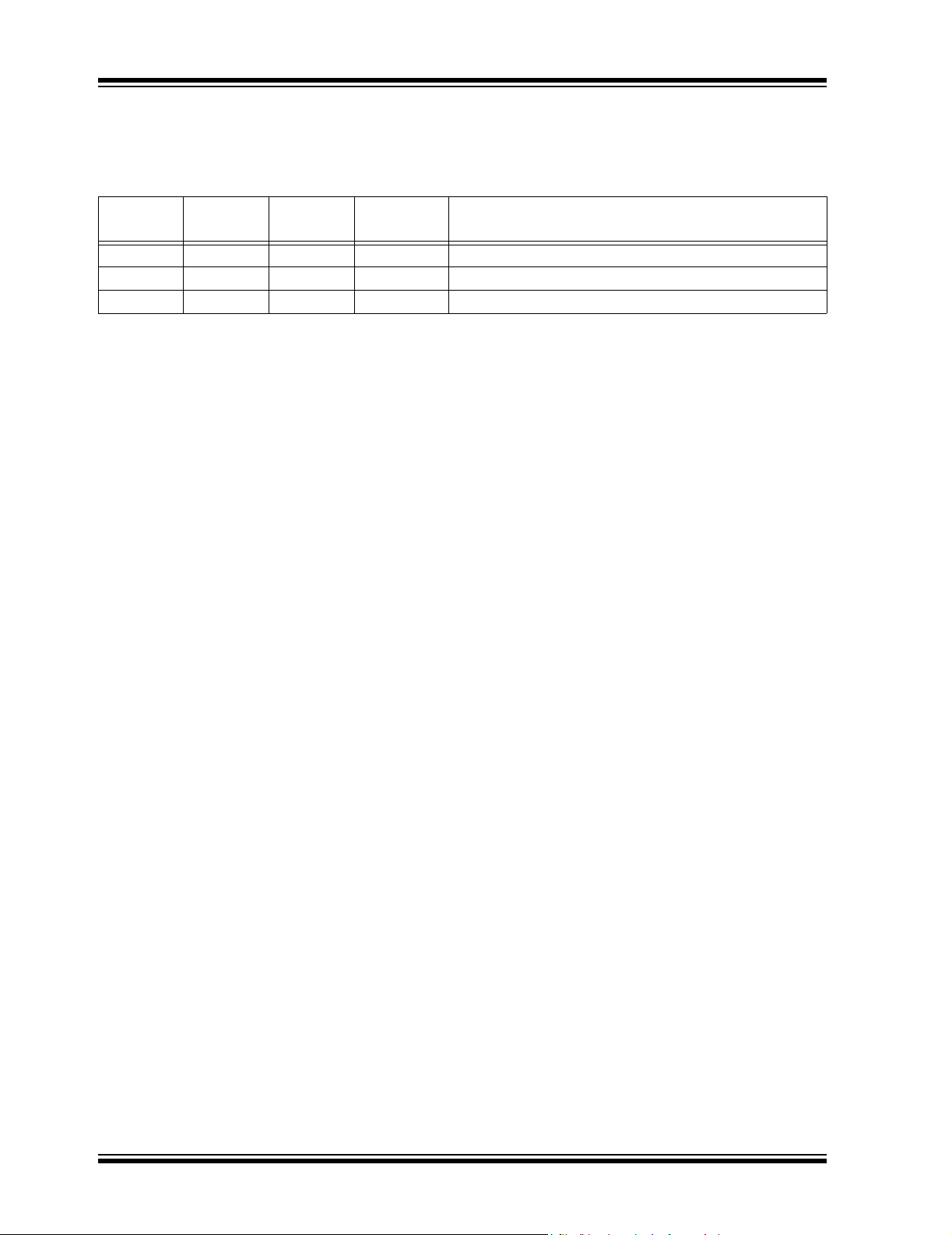
TABLE 3-1: PIN FUNCTION TABLE
Pin No.
SOT-23
1 1 1 GND Ground Terminal
233V
322V
Pin No.
SOT-89
Pin No.
TO-92
Name Function
OUT
IN
Regulated Voltage Output
Unregulated Supply Voltage
3.1 Ground Terminal (GND)
Regulator ground. Tie GND to the negative side of the
output and the negative side of the input capacitor.
Only the LDO bias current (1.6 µA typical) flows out of
this pin; there is no high current. The LDO output
regulation is referenced to this pin. Minimize voltage
drops between this pin and the negative side of the
load.
3.2 Regulated Output Voltage (V
Connect V
positive terminal of the output capacitor. The positive
side of the output capacitor should be physically
located as close to the LDO V
The current flowing out of this pin is equal to the DC
load current.
to the positive side of the load and the
OUT
pin as is practical.
OUT
OUT
)
3.3 Unregulated Input Voltage Pin
)
(V
IN
Connect VIN to the input unregulated source voltage.
Like all low dropout linear regulators, low source
impedance is necessary for the stable operation of the
LDO. The amount of capacitance required to ensure
low source impedance will depend on the proximity of
the input source capacitors or battery type. For most
applications, 1 µF of capacitance will ensure stable
operation of the LDO circuit. For applications that have
load currents below 100 mA, the input capacitance
requirement can be lowered. The type of capacitor
used can be ceramic, tantalum or aluminum
electrolytic. The low ESR characteristics of the ceramic
will yield better noise and PSRR performance at high
frequency.
DS21826B-page 10 © 2007 Microchip Technology Inc.
Page 11
4.0 DETAILED DESCRIPTION
+
-
MCP1700
V
IN
V
OUT
GND
+V
IN
Error Amplifier
Voltage
Reference
Overcurrent
Overtemperature
MCP1700
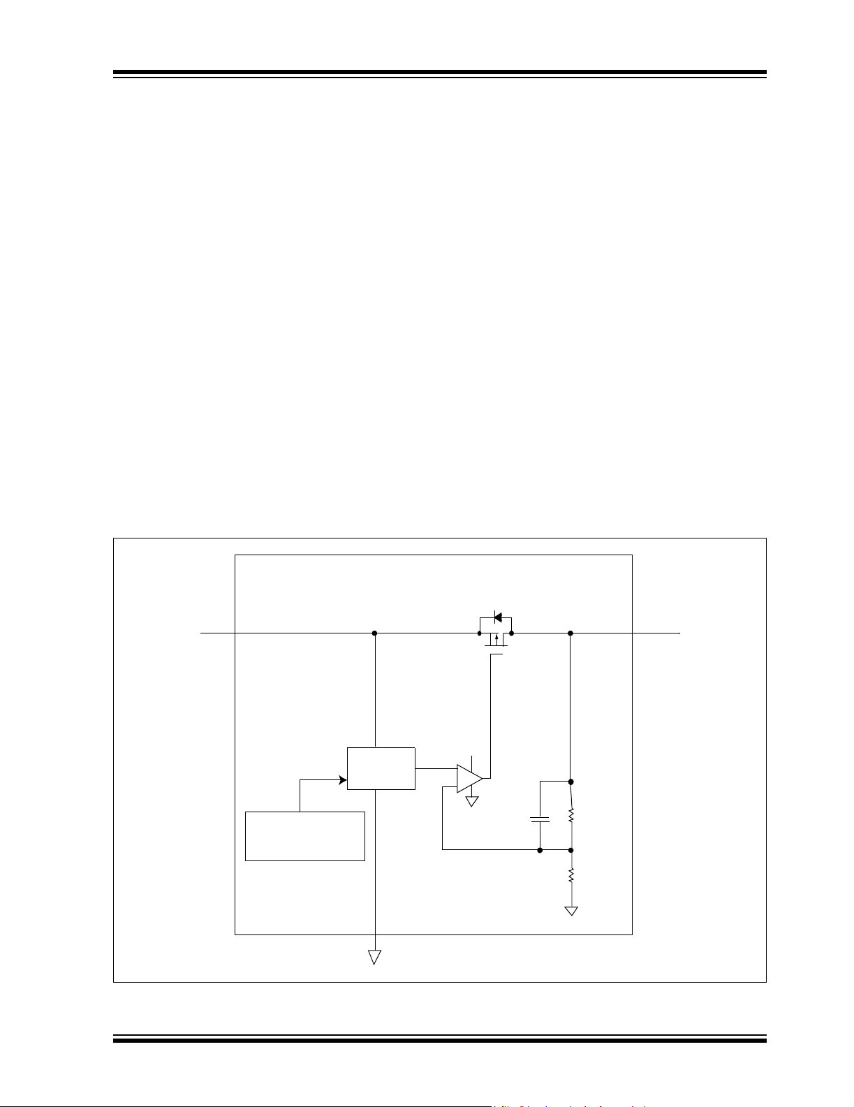
4.1 Output Regulation
A portion of the LDO output voltage is fed back to the
internal error amplifier and compared with the precision
internal bandgap reference. The error amplifier output
will adjust the amount of current that flows through the
P-Channel pass transistor, thus regulating the output
voltage to the desired value. Any changes in input
voltage or output current will cause the error amplifier
to respond and adjust the output voltage to the target
voltage (refer to Figure 4-1).
4.2 Overcurrent
The MCP1700 internal circuitry monitors the amount of
current flowing through the P-Channel pass transistor.
In the event of a short-circuit or excessive output
current, the MCP1700 will turn off the P-Channel
device for a short period, after which the LDO will
attempt to restart. If the excessive current remains, the
cycle will repeat itself.
4.3 Overtemperature
The internal power dissipation within the LDO is a
function of input-to-output voltage differential and load
current. If the power dissipation within the LDO is
excessive, the internal junction temperature will rise
above the typical shutdown threshold of 140°C. At that
point, the LDO will shut down and begin to cool to the
typical turn-on junction temperature of 130°C. If the
power dissipation is low enough, the device will
continue to cool and operate normally. If the power
dissipation remains high, the thermal shutdown
protection circuitry will again turn off the LDO,
protecting it from catastrophic failure.
FIGURE 4-1: Block Diagram.
© 2007 Microchip Technology Inc. DS21826B-page 11
Page 12

MCP1700
5.0 FUNCTIONAL DESCRIPTION
The MCP1700 CMOS low dropout linear regulator is
intended for applications that need the lowest current
consumption while maintaining output voltage
regulation. The operating continuous load range of the
MCP1700 is from 0 mA to 250 mA (V
input operating voltage range is from 2.3V to 6.0V,
making it capable of operating from two, three or four
alkaline cells or a single Li-Ion cell battery input.
5.1 Input
The input of the MCP1700 is connected to the source
of the P-Channel PMOS pass transistor. As with all
LDO circuits, a relatively low source impedance (10Ω)
is needed to prevent the input impedance from causing
the LDO to become unstable. The size and type of the
capacitor needed depends heavily on the input source
type (battery, power supply) and the output current
range of the application. For most applications (up to
100 mA), a 1 µF ceramic capacitor will be sufficient to
ensure circuit stability. Larger values can be used to
improve circuit AC performance.
≥ 2.5V). The
R
5.2 Output
The maximum rated continuous output current for the
MCP1700 is 250 mA (V
where VR< 2.5V, the maximum output current is
200 mA.
A minimum output capacitance of 1.0 µF is required for
small signal stability in applications that have up to
250 mA output current capability. The capacitor type
can be ceramic, tantalum or aluminum electrolytic. The
esr range on the output capacitor can range from 0Ω to
2.0Ω.
≥ 2.5V). For applications
R
5.3 Output Rise time
When powering up the internal reference output, the
typical output rise time of 500 µs is controlled to
prevent overshoot of the output voltage.
DS21826B-page 12 © 2007 Microchip Technology Inc.
Page 13
MCP1700
MCP1700
GND
V
OUT
V
IN
C
IN
1µF Ceramic
C
OUT
1 µF Ceramic
V
OUT
V
IN
(2.3V to 3.2V)
1.8V
I
OUT
150 mA
P
LDO
V
IN MAX)()VOUT MIN()
–()I
OUT MAX )()
×=
P
LDO
= LDO Pass device internal power dissipation
V
IN(MAX)
= Maximum input voltage
V
OUT(MIN)
= LDO minimum output voltage
T
JMAX()PTOTAL
RθJA× T
AMAX
+=
T
J(MAX)
= Maximum continuous junction
temperature.
P
TOTAL
= Total device power dissipation.
Rθ
JA
= Thermal resistance from junction to ambient.
T
AMAX
= Maximum ambient temperature.
P
DMAX()
T
JMAX()TAMAX()
–()
Rθ
JA
---------------------------------------------------=
P
D(MAX)
= Maximum device power dissipation.
T
J(MAX)
= Maximum continuous junction
temperature.
T
A(MAX)
= Maximum ambient temperature.
Rθ
JA
= Thermal resistance from junction to ambient.
T
JRISE()PDMAX()RθJA
×=
T
J(RISE)
= Rise in device junction temperature over
the ambient temperature.
P
TOTAL
= Maximum device power dissipation.
Rθ
JA
= Thermal resistance from junction to ambient.
TJT
JRISE()TA
+=
T
J
= Junction Temperature.
T
J(RISE)
= Rise in device junction temperature over
the ambient temperature.
T
A
= Ambient temperature.
6.0 APPLICATION CIRCUITS & ISSUES
6.1 Typical Application
The MCP1700 is most commonly used as a voltage
regulator. It’s low quiescent current and low dropout
voltage make it ideal for many battery-powered
applications.
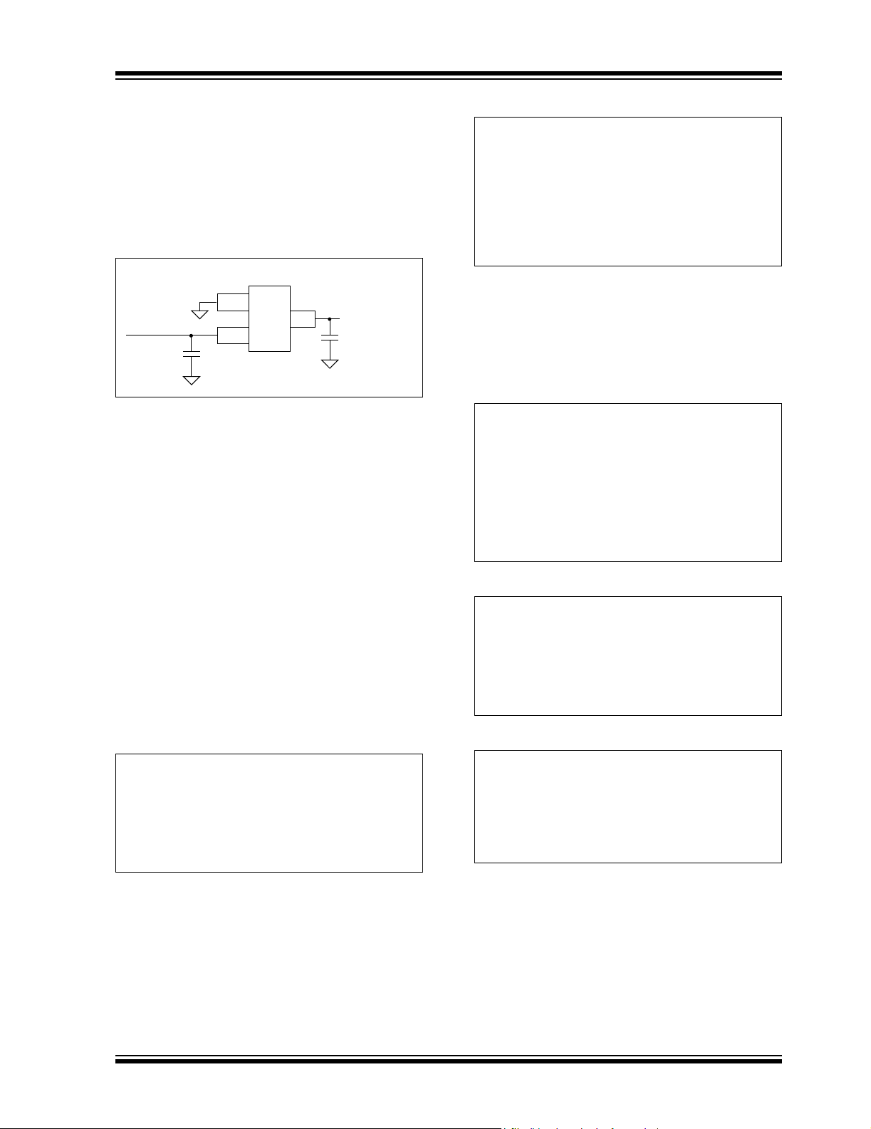
FIGURE 6-1: Typical Application Circuit.
6.1.1 APPLICATION INPUT CONDITIONS
Package Type = SOT-23
Input Voltage Range = 2.3V to 3.2V
V
maximum = 3.2V
IN
V
typical = 1.8V
OUT
I
= 150 mA maximum
OUT
EQUATION 6-2:
The maximum power dissipation capability for a
package can be calculated given the junction-toambient thermal resistance and the maximum ambient
temperature for the application. The following equation
can be used to determine the package maximum
internal power dissipation.
EQUATION 6-3:
6.2 Power Calculations
6.2.1 POWER DISSIPATION
The internal power dissipation of the MCP1700 is a
function of input voltage, output voltage and output
current. The power dissipation, as a result of the
quiescent current draw, is so low, it is insignificant
(1.6 µA x V
calculate the internal power dissipation of the LDO.
EQUATION 6-1:
The maximum continuous operating junction
temperature specified for the MCP1700 is +125
estimate the internal junction temperature of the
MCP1700, the total internal power dissipation is
multiplied by the thermal resistance from junction to
ambient (Rθ
ambient for the SOT-23 pin package is estimated at
230
°C/W.
© 2007 Microchip Technology Inc. DS21826B-page 13
). The following equation can be used to
IN
). The thermal resistance from junction to
JA
EQUATION 6-4:
EQUATION 6-5:
°C. To
Page 14
MCP1700
PIC
®
MCP1700
GND
V
IN
C
IN
1µF
C
OUT
1µF
Bridge Sensor
V
OUT
V
REF
ADO
AD1
Ratio Metric Reference
1 µA Bias
Microcontroller
6.3 Voltage Regulator
Internal power dissipation, junction temperature rise,
junction temperature and maximum power dissipation
are calculated in the following example. The power
dissipation, as a result of ground current, is small
enough to be neglected.
6.3.1 POWER DISSIPATION EXAMPLE
Package
Package Type = SOT-23
Input Voltage
V
= 2.3V to 3.2V
IN
LDO Output Voltages and Currents
V
=1.8V
OUT
I
=150mA
OUT
Maximum Ambient Temperature
T
= +40°C
A(MAX)
Internal Power Dissipation
Internal Power dissipation is the product of the LDO
output current times the voltage across the LDO
(V
IN
to V
P
).
OUT
LDO(MAX)
P
LDO
P
LDO
=(V
IN(MAX)
- V
OUT(MIN)
) x I
OUT(MAX)
= (3.2V - (0.97 x 1.8V)) x 150 mA
= 218.1 milli-Watts
Maximum Package Power Dissipation at +40°C
Ambient Temperature
SOT-23 (230.0°C/Watt = Rθ
SOT-89 (52°C/Watt = Rθ
TO-92 (131.9°C/Watt = Rθ
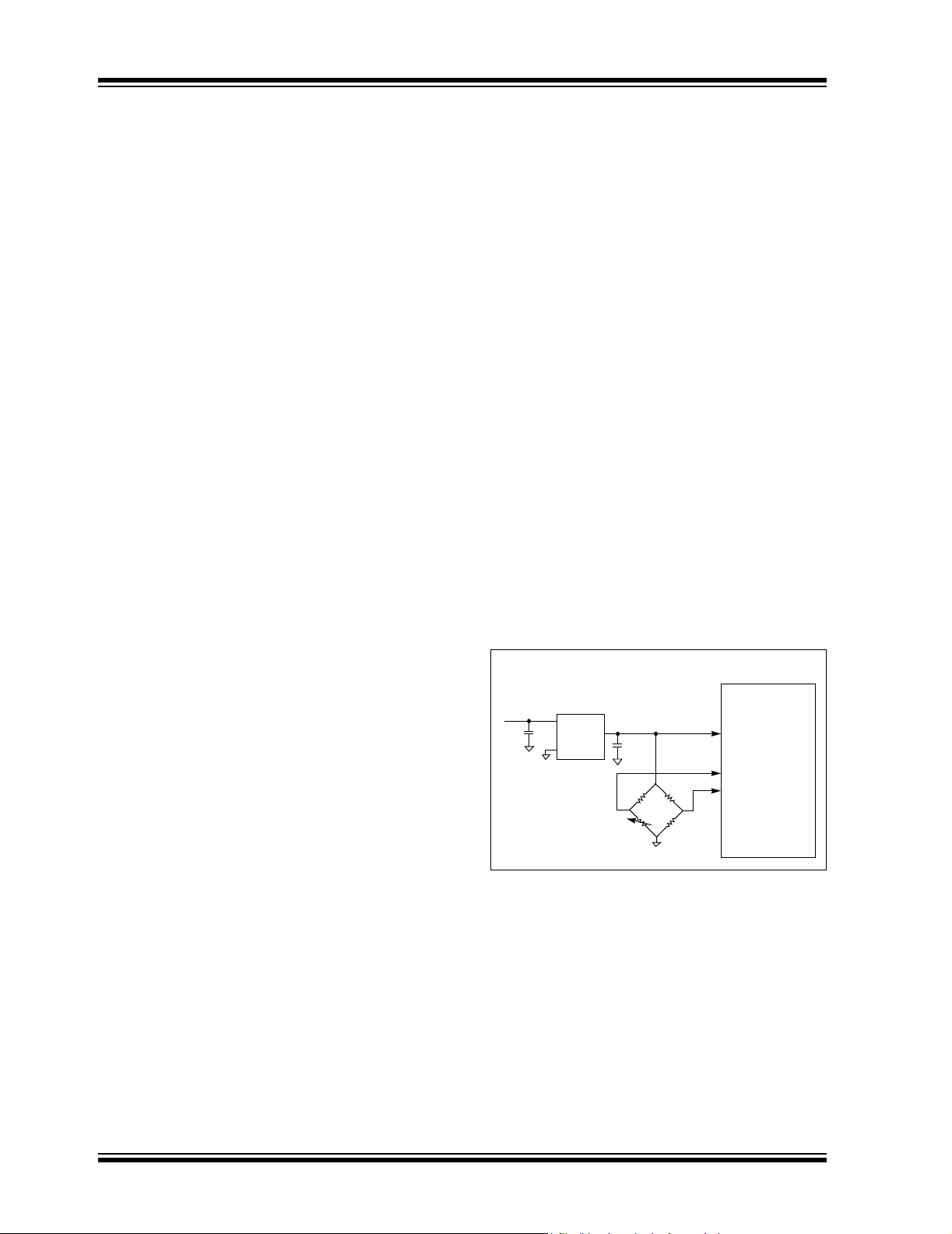
6.4 Voltage Reference
The MCP1700 can be used not only as a regulator, but
also as a low quiescent current voltage reference. In
many microcontroller applications, the initial accuracy
of the reference can be calibrated using production test
equipment or by using a ratio measurement. When the
initial accuracy is calibrated, the thermal stability and
line regulation tolerance are the only errors introduced
by the MCP1700 LDO. The low cost, low quiescent
current and small ceramic output capacitor are all
P
D(MAX)
P
D(MAX)
P
D(MAX)
P
D(MAX)
P
D(MAX)
P
D(MAX)
T
=T
J
JRISE
+ T
A(MAX)
TJ = 90.2°C
)
JA
= (125°C - 40°C) / 230°C/W
= 369.6 milli-Watts
)
JA
= (125°C - 40°C) / 52°C/W
= 1.635 Watts
)
JA
= (125°C - 40°C) / 131.9°C/W
= 644 milli-Watts
advantages when using the MCP1700 as a voltage
Device Junction Temperature Rise
reference.
The internal junction temperature rise is a function of
internal power dissipation and the thermal resistance
from junction to ambient for the application. The thermal
resistance from junction to ambient (Rθ
) is derived
JA
from an EIA/JEDEC standard for measuring thermal
resistance for small surface mount packages. The EIA/
JEDEC specification is JESD51-7, “High Effective
Thermal Conductivity Test Board for Leaded Surface
Mount Packages”. The standard describes the test
method and board specifications for measuring the
thermal resistance from junction to ambient. The actual
thermal resistance for a particular application can vary
depending on many factors, such as copper area and
thickness. Refer to AN792, “A Method to Determine
How Much Power a SOT-23 Can Dissipate in an
Application”, (DS00792), for more information regarding
FIGURE 6-2: Using the MCP1700 as a voltage reference.
this subject.
T
Junction Temperature Estimate
=P
J(RISE)
T
= 218.1 milli-Watts x 230.0°C/Watt
JRISE
T
= 50.2°C
JRISE
To estimate the internal junction temperature, the
calculated temperature rise is added to the ambient or
offset temperature. For this example, the worst-case
junction temperature is estimated below.
DS21826B-page 14 © 2007 Microchip Technology Inc.
x Rq
TOTAL
JA
6.5 Pulsed Load Applications
For some applications, there are pulsed load current
events that may exceed the specified 250 mA
maximum specification of the MCP1700. The internal
current limit of the MCP1700 will prevent high peak
load demands from causing non-recoverable damage.
The 250 mA rating is a maximum average continuous
rating. As long as the average current does not exceed
250 mA, pulsed higher load currents can be applied to
the MCP1700
MCP1700 is 550 mA (T
. The typical current limit for the
+25°C).
A
Page 15
7.0 PACKAGING INFORMATION
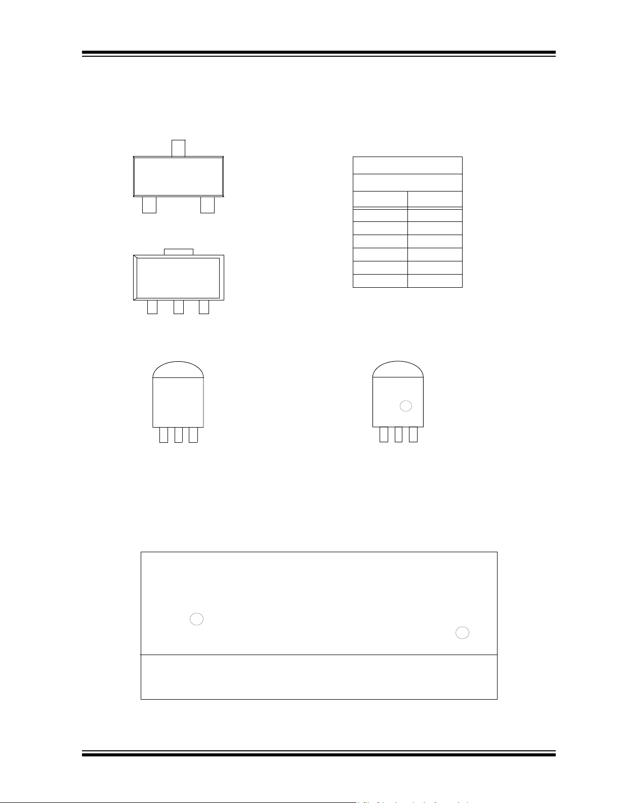
3-Pin SOT-23
CKNN
3-Pin SOT-89
CUYYWW
NNN
3-Pin TO-92
XXXXXX
XXXXXX
YWWNNN
Standard
Extended Temp
Symbol Voltage *
CK 1.2
CM 1.8
CP 2.5
CR 3.0
CS 3.3
CU 5.0
Example:
1700
1202E
313256
* Custom output voltages available upon request.
Contact your local Microchip sales office for more
information.
XXXXXX
TO^^
Legend: XX...X Customer-specific information
Y Year code (last digit of calendar year)
YY Year code (last 2 digits of calendar year)
WW Week code (week of January 1 is week ‘01’)
NNN Alphanumeric traceability code
Pb-free JEDEC designator for Matte Tin (Sn)
* This package is Pb-free. The Pb-free JEDEC designator ( )
can be found on the outer packaging for this package.
Note: In the event the full Microchip part number cannot be marked on one line, it will
be carried over to the next line, thus limiting the number of available
characters for customer-specific information.
3
e
3
e
7.1 Package Marking Information
MCP1700
3
e
© 2007 Microchip Technology Inc. DS21826B-page 15
Page 16
MCP1700
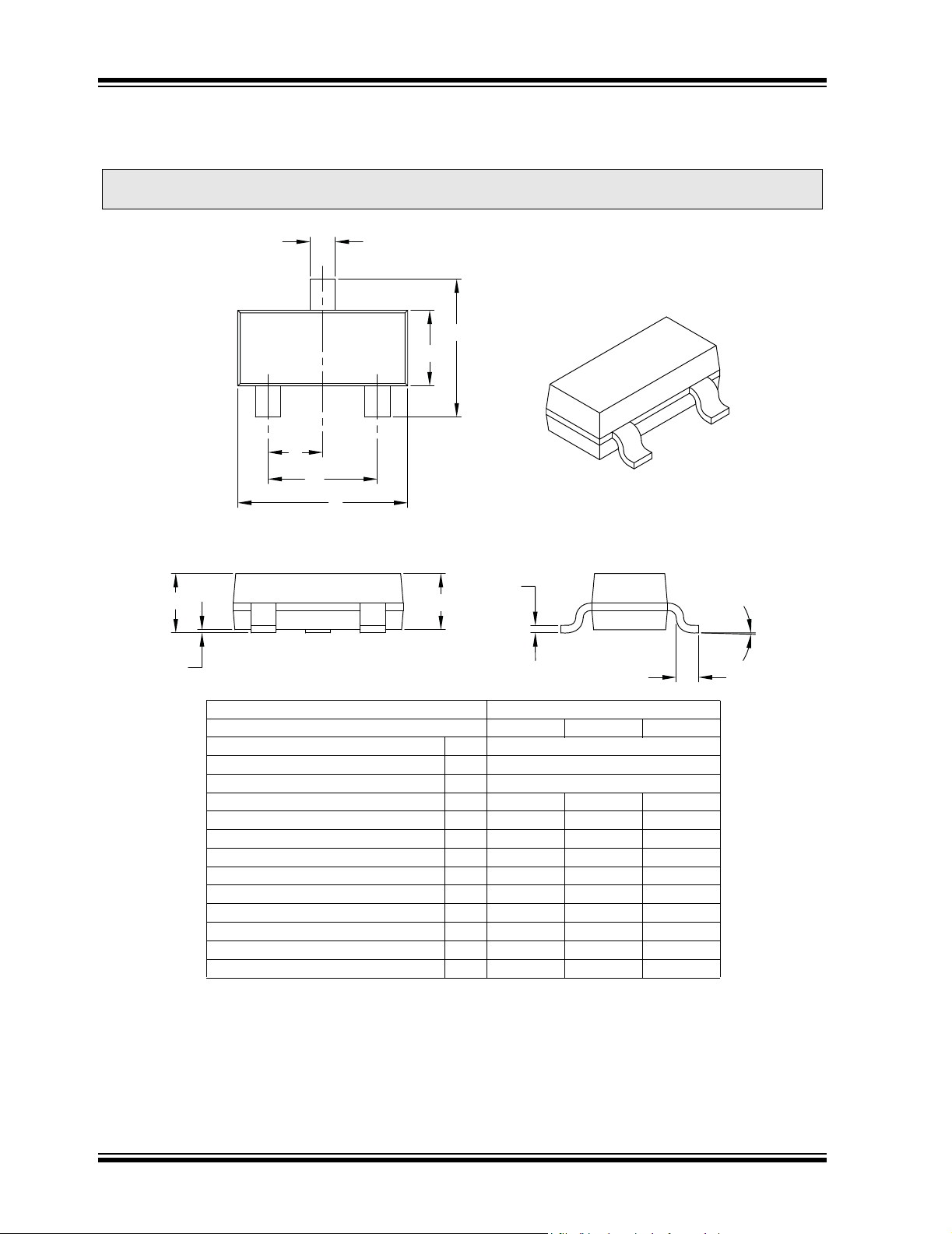
3-Lead Plastic Small Outline Transistor (TT or NB) [SOT-23]
Notes:
1. Dimensions D and E1 do not include mold flash or protrusions. Mold flash or protrusions shall not exceed 0.25 mm per side.
2. Dimensioning and tolerancing per ASME Y14.5M.
BSC: Basic Dimension. Theoretically exact value shown without tolerances.
Note: For the most current package drawings, please see the Microchip Packaging Specification located at
http://www.microchip.com/packaging
Units MILLIMETERS
Dimension Limits MIN NOM MAX
Number of Pins N 3
Lead Pitch e 0.95 BSC
Outside Lead Pitch e1 1.90 BSC
Overall Height A 0.89 – 1.12
Molded Package Thickness A2 0.79 0.95 1.02
Standoff A1 0.01 – 0.10
Overall Width E 2.10 – 2.64
Molded Package Width E1 1.16 1.30 1.40
Overall Length D 2.67 2.90 3.05
Foot Length L 0.13 0.50 0.60
Foot Angle φ 0° – 10°
Lead Thickness c 0.08 – 0.20
Lead Width b 0.30 – 0.54
b
N
E
E1
2
1
e
e1
D
A
A1
A2
c
L
φ
Microchip Technology Drawing C04-104B
DS21826B-page 16 © 2007 Microchip Technology Inc.
Page 17
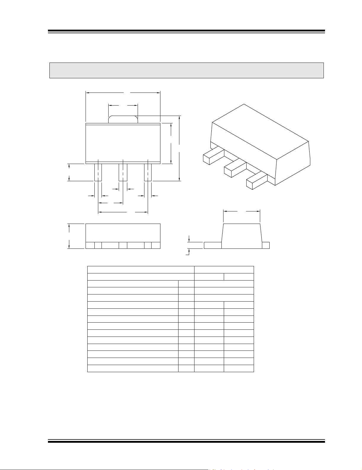
3-Lead Plastic Small Outline Transistor Header (MB) [SOT-89]
Notes:
1. Dimensions D and E do not include mold flash or protrusions. Mold flash or protrusions shall not exceed 0.127 mm per side.
2. Dimensioning and tolerancing per ASME Y14.5M.
BSC: Basic Dimension. Theoretically exact value shown without tolerances.
Note: For the most current package drawings, please see the Microchip Packaging Specification located at
http://www.microchip.com/packaging
Units MILLIMETERS
Dimension Limits MIN MAX
Number of Leads N 3
Pitch e 1.50 BSC
Outside Lead Pitch e1 3.00 BSC
Overall Height A 1.40 1.60
Overall Width H 3.94 4.25
Molded Package Width at Base E 2.29 2.60
Molded Package Width at Top E1 2.13 2.29
Overall Length D 4.39 4.60
Tab Length D1 1.40 1.83
Foot Length L 0.79 1.20
Lead Thickness c 0.35 0.44
Lead 2 Width b 0.41 0.56
Leads 1 & 3 Width b1 0 .36 0.48
D
D1
E
H
N
b1
e1
b
21
e
b1
L
A
C
E1
Microchip Technology Drawing C04-029B
MCP1700
© 2007 Microchip Technology Inc. DS21826B-page 17
Page 18
MCP1700
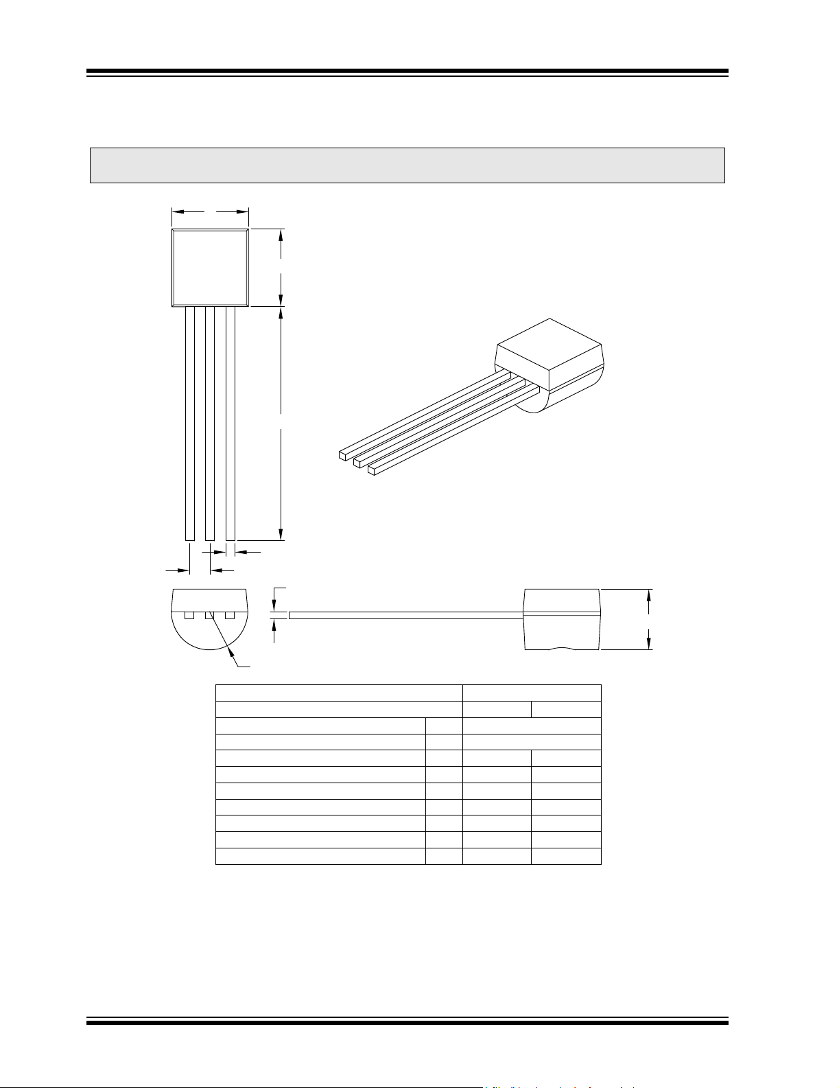
3-Lead Plastic Transistor Outline (TO or ZB) [TO-92]
Notes:
1. Dimensions A and E do not include mold flash or protrusions. Mold flash or protrusions shall not exceed .005" per side.
2. Dimensioning and tolerancing per ASME Y14.5M.
BSC: Basic Dimension. Theoretically exact value shown without tolerances.
Note: For the most current package drawings, please see the Microchip Packaging Specification located at
http://www.microchip.com/packaging
Units INCHES
Dimension Limits MIN MAX
Number of Pins N 3
Pitch e .050 BSC
Bottom to Package Flat D .125 .165
Overall Width E .175 .205
Overall Length A .170 .210
Molded Package Radius R .080 .105
Tip to Seating Plane L .500 –
Lead Thickness c .014 .021
Lead Width b .014 .022
E
A
N
1
L
b
e
c
R
D
1
2
3
Microchip Technology Drawing C04-101B
DS21826B-page 18 © 2007 Microchip Technology Inc.
Page 19

APPENDIX A: REVISION HISTORY
Revision B (February 2007)
• Updated Packaging Information.
• Corrected Section “Product Identification
System”.
• Changed X5R to X7R in Notes to “DC
Characteristics”, “Temperature
Specifications”, and “Typical Performance
Curves” .
Revision A (November 2005)
• Original Release of this Document.
MCP1700
© 2007 Microchip Technology Inc. DS21826B-page 19
Page 20

MCP1700
NOTES:
DS21826B-page 20 © 2007 Microchip Technology Inc.
Page 21
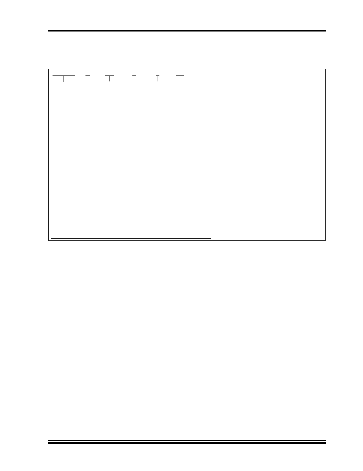
PRODUCT IDENTIFICATION SYSTEM
Device: MCP1700: Low Quiescent Current LDO
Tape and Reel: T: Tape and Reel only applies to SOT-23 and SOT-89
devices
Standard Output
Voltage: *
120 = 1.2V
180 = 1.8V
250 = 2.5V
300 = 3.0V
330 = 3.3V
500 = 5.0V
* Custom output voltages available upon request. Contact
your local Microchip sales office for more information
Tolerance: 2 = 2%
Temperature Range: E = -40°C to +125°C (Extended)
Package: MB = Plastic Small Outline Transistor (SOT-89), 3-lead
TO = Plastic Small Outline Transistor (TO-92), 3-lead
TT = Plastic Small Outline Transistor SOT-23), 3-lead
Examples:
SOT-89 Package:
a) MCP1700T-1202E/MB: 1.2V V
OUT
b) MCP1700T-1802E/MB: 1.8V V
OUT
c) MCP1700T-2502E/MB: 2.5V V
OUT
d) MCP1700T-3002E/MB: 3.0V V
OUT
e) MCP1700T-3302E/MB: 3.3V V
OUT
f) MCP1700T-5002E/MB: 5.0V V
OUT
TO-92 Package:
g) MCP1700-1202E/TO: 1.2V V
OUT
h) MCP1700-1802E/TO: 1.8V V
OUT
i) MCP1700-2502E/TO: 2.5V V
OUT
j) MCP1700-3002E/TO: 3.0V V
OUT
k) MCP1700-3302E/TO: 3.3V V
OUT
l) MCP1700-5002E/TO: 5.0V V
OUT
SOT-23 Package:
a) MCP1700T-1202E/TT: 1.2V V
OUT
b) MCP1700T-1802E/TT: 1.8V V
OUT
c) MCP1700T-2502E/TT: 2.5V V
OUT
d) MCP1700T-3002E/TT: 3.0V V
OUT
e) MCP1700T-3302E/TT: 3.3V V
OUT
f) MCP1700T-5002E/TT: 5.0V V
OUT
PART NO. X- XXX
Vol tag eTap e &
Reel
MCP1700
X
Tol eranceXTem p.
Range
/XX
Package
Output
To order or obtain information, e.g., on pricing or delivery, refer to the factory or the listed sales office.
MCP1700
© 2007 Microchip Technology Inc. DS21826B-page 21
Page 22

MCP1700
NOTES:
DS21826B-page 22 © 2007 Microchip Technology Inc.
Page 23

Note the following details of the code protection feature on Microchip devices:
• Microchip products meet the specification contained in their particular Microchip Data Sheet.
• Microchip believes that its family of products is one of the most secure families of its kind on the market today, when used in the
intended manner and under normal conditions.
• There are dishonest and possibly illegal methods used to breach the code protection feature. All of these methods, to our
knowledge, require using the Microchip products in a manner outside the operating specifications contained in Microchip’s Data
Sheets. Most likely, the person doing so is engaged in theft of intellectual property.
• Microchip is willing to work with the customer who is concerned about the integrity of their code.
• Neither Microchip nor any other semiconductor manufacturer can guarantee the security of their code. Code protection does not
mean that we are guaranteeing the product as “unbreakable.”
Code protection is constantly evolving. We at Microchip are committed to continuously improving the code protection features of our
products. Attempts to break Microchip’s code protection feature may be a violation of the Digital Millennium Copyright Act. If such acts
allow unauthorized access to your software or other copyrighted work, you may have a right to sue for relief under that Act.
Information contained in this publication regarding device
applications and the like is provided only for your convenience
and may be superseded by updates. It is your responsibility to
ensure that your application meets with your specifications.
MICROCHIP MAKES NO REPRESENTATIONS OR
WARRANTIES OF ANY KIND WHETHER EXPRESS OR
IMPLIED, WRITTEN OR ORAL, STATUTORY OR
OTHERWISE, RELATED TO THE INFORMATION,
INCLUDING BUT NOT LIMITED TO ITS CONDITION,
QUALITY, PERFORMANCE, MERCHANTABILITY OR
FITNESS FOR PURPOSE. Microchip disclaims all liability
arising from this information and its use. Use of Microchip
devices in life support and/or safety applications is entirely at
the buyer’s risk, and the buyer agrees to defend, indemnify and
hold harmless Microchip from any and all damages, claims,
suits, or expenses resulting from such use. No licenses are
conveyed, implicitly or otherwise, under any Microchip
intellectual property rights.
Trademarks
The Microchip name and logo, the Microchip logo, Accuron,
dsPIC, K
EELOQ, KEELOQ logo, microID, MPLAB, PIC,
PICmicro, PICSTART, PRO MATE, PowerSmart, rfPIC, and
SmartShunt are registered trademarks of Microchip
Technology Incorporated in the U.S.A. and other countries.
AmpLab, FilterLab, Linear Active Thermistor, Migratable
Memory, MXDEV, MXLAB, PS logo, SEEVAL, SmartSensor
and The Embedded Control Solutions Company are
registered trademarks of Microchip Technology Incorporated
in the U.S.A.
Analog-for-the-Digital Age, Application Maestro, CodeGuard,
dsPICDEM, dsPICDEM.net, dsPICworks, ECAN,
ECONOMONITOR, FanSense, FlexROM, fuzzyLAB,
In-Circuit Serial Programming, ICSP, ICEPIC, Mindi, MiWi,
MPASM, MPLAB Certified logo, MPLIB, MPLINK, PICkit,
PICDEM, PICDEM.net, PICLAB, PICtail, PowerCal,
PowerInfo, PowerMate, PowerTool, REAL ICE, rfLAB,
rfPICDEM, Select Mode, Smart Serial, SmartTel, Total
Endurance, UNI/O, WiperLock and ZENA are trademarks of
Microchip Technology Incorporated in the U.S.A. and other
countries.
SQTP is a service mark of Microchip Technology Incorporated
in the U.S.A.
All other trademarks mentioned herein are property of their
respective companies.
© 2007, Microchip Technology Incorporated, Printed in the
U.S.A., All Rights Reserved.
Printed on recycled paper.
Microchip received ISO/TS-16949:2002 certification for its worldwide
headquarters, design and wafer fabrication facilities in Chandler and
Tempe, Arizona, Gresham, Oregon and Mountain View, California. The
Company’s quality system processes and procedures are for its PIC
MCUs and dsPIC® DSCs, KEELOQ
EEPROMs, microperipherals, nonvolatile memory and analog
products. In addition, Microchip’s quality system for the design and
manufacture of development systems is ISO 9001:2000 certified.
®
code hopping devices, Serial
© 2007 Microchip Technology Inc. DS21826B-page 23
®
Page 24

WORLDWIDE SALES AND SERVICE
AMERICAS
Corporate Office
2355 West Chandler Blvd.
Chandler, AZ 85224-6199
Tel: 480-792-7200
Fax: 480-792-7277
Technical Support:
http://support.microchip.com
Web Address:
www.microchip.com
Atlanta
Duluth, GA
Tel: 678-957-9614
Fax: 678-957-1455
Boston
Westborough, MA
Tel: 774-760-0087
Fax: 774-760-0088
Chicago
Itasca, IL
Tel: 630-285-0071
Fax: 630-285-0075
Dallas
Addison, TX
Tel: 972-818-7423
Fax: 972-818-2924
Detroit
Farmington Hills, MI
Tel: 248-538-2250
Fax: 248-538-2260
Kokomo
Kokomo, IN
Tel: 765-864-8360
Fax: 765-864-8387
Los Angeles
Mission Viejo, CA
Tel: 949-462-9523
Fax: 949-462-9608
Santa Clara
Santa Clara, CA
Tel: 408-961-6444
Fax: 408-961-6445
Toronto
Mississauga, Ontario,
Canada
Tel: 905-673-0699
Fax: 905-673-6509
ASIA/PACIFIC
Asia Pacific Office
Suites 3707-14, 37th Floor
Tower 6, The Gateway
Habour City, Kowloon
Hong Kong
Tel: 852-2401-1200
Fax: 852-2401-3431
Australia - Sydney
Tel: 61-2-9868-6733
Fax: 61-2-9868-6755
China - Beijing
Tel: 86-10-8528-2100
Fax: 86-10-8528-2104
China - Chengdu
Tel: 86-28-8665-5511
Fax: 86-28-8665-7889
China - Fuzhou
Tel: 86-591-8750-3506
Fax: 86-591-8750-3521
China - Hong Kong SAR
Tel: 852-2401-1200
Fax: 852-2401-3431
China - Qingdao
Tel: 86-532-8502-7355
Fax: 86-532-8502-7205
China - Shanghai
Tel: 86-21-5407-5533
Fax: 86-21-5407-5066
China - Shenyang
Tel: 86-24-2334-2829
Fax: 86-24-2334-2393
China - Shenzhen
Tel: 86-755-8203-2660
Fax: 86-755-8203-1760
China - Shunde
Tel: 86-757-2839-5507
Fax: 86-757-2839-5571
China - Wuhan
Tel: 86-27-5980-5300
Fax: 86-27-5980-5118
China - Xian
Tel: 86-29-8833-7250
Fax: 86-29-8833-7256
ASIA/PACIFIC
India - Bangalore
Tel: 91-80-4182-8400
Fax: 91-80-4182-8422
India - New Delhi
Tel: 91-11-4160-8631
Fax: 91-11-4160-8632
India - Pune
Tel: 91-20-2566-1512
Fax: 91-20-2566-1513
Japan - Yokohama
Tel: 81-45-471- 6166
Fax: 81-45-471-6122
Korea - Gumi
Tel: 82-54-473-4301
Fax: 82-54-473-4302
Korea - Seoul
Tel: 82-2-554-7200
Fax: 82-2-558-5932 or
82-2-558-5934
Malaysia - Penang
Tel: 60-4-646-8870
Fax: 60-4-646-5086
Philippines - Manila
Tel: 63-2-634-9065
Fax: 63-2-634-9069
Singapore
Tel: 65-6334-8870
Fax: 65-6334-8850
Taiwan - Hsin Chu
Tel: 886-3-572-9526
Fax: 886-3-572-6459
Taiwan - Kaohsiung
Tel: 886-7-536-4818
Fax: 886-7-536-4803
Taiwan - Taipei
Tel: 886-2-2500-6610
Fax: 886-2-2508-0102
Thailand - Bangkok
Tel: 66-2-694-1351
Fax: 66-2-694-1350
EUROPE
Austria - Wels
Tel: 43-7242-2244-39
Fax: 43-7242-2244-393
Denmark - Copenhagen
Tel: 45-4450-2828
Fax: 45-4485-2829
France - Paris
Tel: 33-1-69-53-63-20
Fax: 33-1-69-30-90-79
Germany - Munich
Tel: 49-89-627-144-0
Fax: 49-89-627-144-44
Italy - Milan
Tel: 39-0331-742611
Fax: 39-0331-466781
Netherlands - Drunen
Tel: 31-416-690399
Fax: 31-416-690340
Spain - Madrid
Tel: 34-91-708-08-90
Fax: 34-91-708-08-91
UK - Wokingham
Tel: 44-118-921-5869
Fax: 44-118-921-5820
12/08/06
DS21826B-page 24 © 2007 Microchip Technology Inc.
 Loading...