

Page 1
Philips Semiconductors Advanced BiCMOS Products Product specification
MB2841Dual 10-bit bus interface latch (3-State)
1
August 24, 1993 853-1668 10619
FEATURES
•High speed parallel latches
•Live insertion/extraction permitted
•Extra data width for wide address/data
paths or buses carrying parity
•Power-up 3-State
•Power-up reset
•Ideal where high speed, light loading, or
increased fan-in are required with MOS
microprocessors
•Output capability: +64mA/–32mA
•Latch-up protection exceeds 500mA per
Jedec JC40.2 Std 17
•ESD protection exceeds 2000V per MIL
STD 883 Method 3015 and 200V per
Machine Model
DESCRIPTION
The MB2841 Bus interface register is
designed to provide extra data width for wider
data/address paths of buses carrying parity.
The MB2841 consists of two sets of ten
D-type latches with 3-State outputs. The
flip-flops appear transparent to the data when
Latch Enable (nLE) is High. This allows
asynchronous operation, as the output
transition follows the data in transition. On the
nLE High-to-Low transition, the data that
meets the setup and hold time is latched.
Data appears on the bus when the Output
Enable (nOE
) is Low. When nOE is High the
output is in the High-impedance state.
QUICK REFERENCE DATA
SYMBOL PARAMETER
CONDITIONS
T
amb
= 25°C; GND = 0V
TYPICAL UNIT
t
PLH
t
PHL
Propagation delay
nDx to nQx
CL = 50pF; VCC = 5V 3.5 ns
C
IN
Input capacitance VI = 0V or V
CC
4 pF
C
OUT
Output capacitance VO = 0V or VCC; 3-State 7 pF
I
CCZ
Total supply current Outputs disabled; VCC = 5.5V 120 µA
ORDERING INFORMATION
PACKAGES TEMPERATURE RANGE ORDER CODE DRAWING NUMBER
52-pin Plastic Quad Flat Pack (PQFP) -40°C to +85°C MB2841BB 1418B
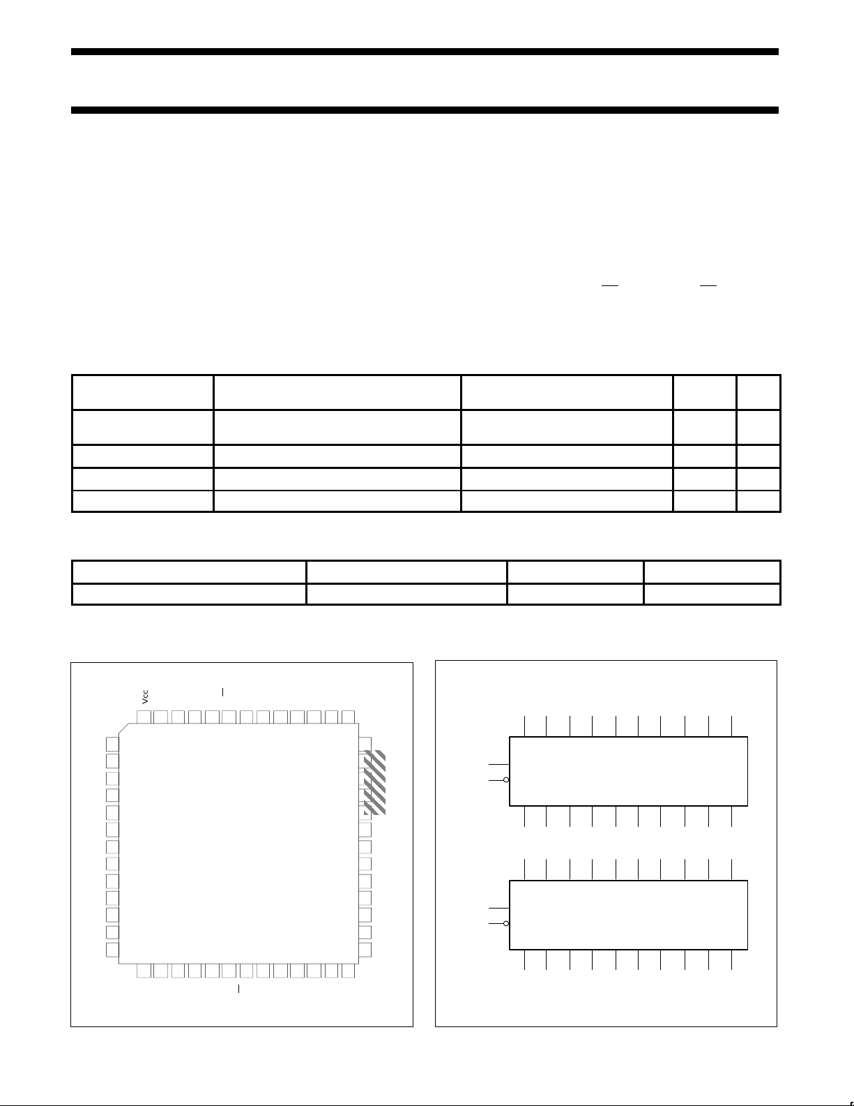
PIN CONFIGURATION LOGIC SYMBOL
5
Vcc
1Q3
1Q2
1Q1
1Q0
1OE
1LE
1D0
1D1
GND
1D2
1D3
Vcc
Vcc
2Q6
2Q7
GND
2Q8
2Q9
2OE
2LE
2D9
2D8
2D7
2D6
Vcc
19 2220 231716 25 26241514 2118
1Q8
2Q1
1Q9
2Q2
GND
1Q6
2Q4
2Q5
2Q3
1Q5
2Q0
1Q7
1Q4
1
2
3
4
6
7
8
9
10
11
12
13
47 4446 434950 41 40425152 4548
1D9
2D2
2D0
GND
1D7
1D6
2D4
2D5
2D3
1D5
2D1
1D8
1D439
38
37
36
35
34
33
32
31
30
29
28
27
MB2841
52-pin PQFP
45 44 42 41 39 38 37 36
1D0 1D1 1D2 1D3 1D4 1D5 1D6 1D7
1Q0 1Q1 1Q2 1Q3 1Q4 1Q5 1Q6 1Q7
48 49 50 51 1 2 3 5
46
47
1LE
1OE
35 34
1D8 1D9
1Q8 1Q9
6 7
33 32 31 29 28 27 25 24
2D0 2D1 2D2 2D3 2D4 2D5 2D6 2D7
2Q0 2Q1 2Q2 2Q3 2Q4 2Q5 2Q6 2Q7
8 9 10 11 12 13 15 16
21
20
2LE
2OE
23 22
2D8 2D9
2Q8 2Q9
18 19
È
È
È
Page 2
Philips Semiconductors Advanced BiCMOS Products Product specification
MB2841Dual 10-bit bus interface latch (3-State)
August 24, 1993
2
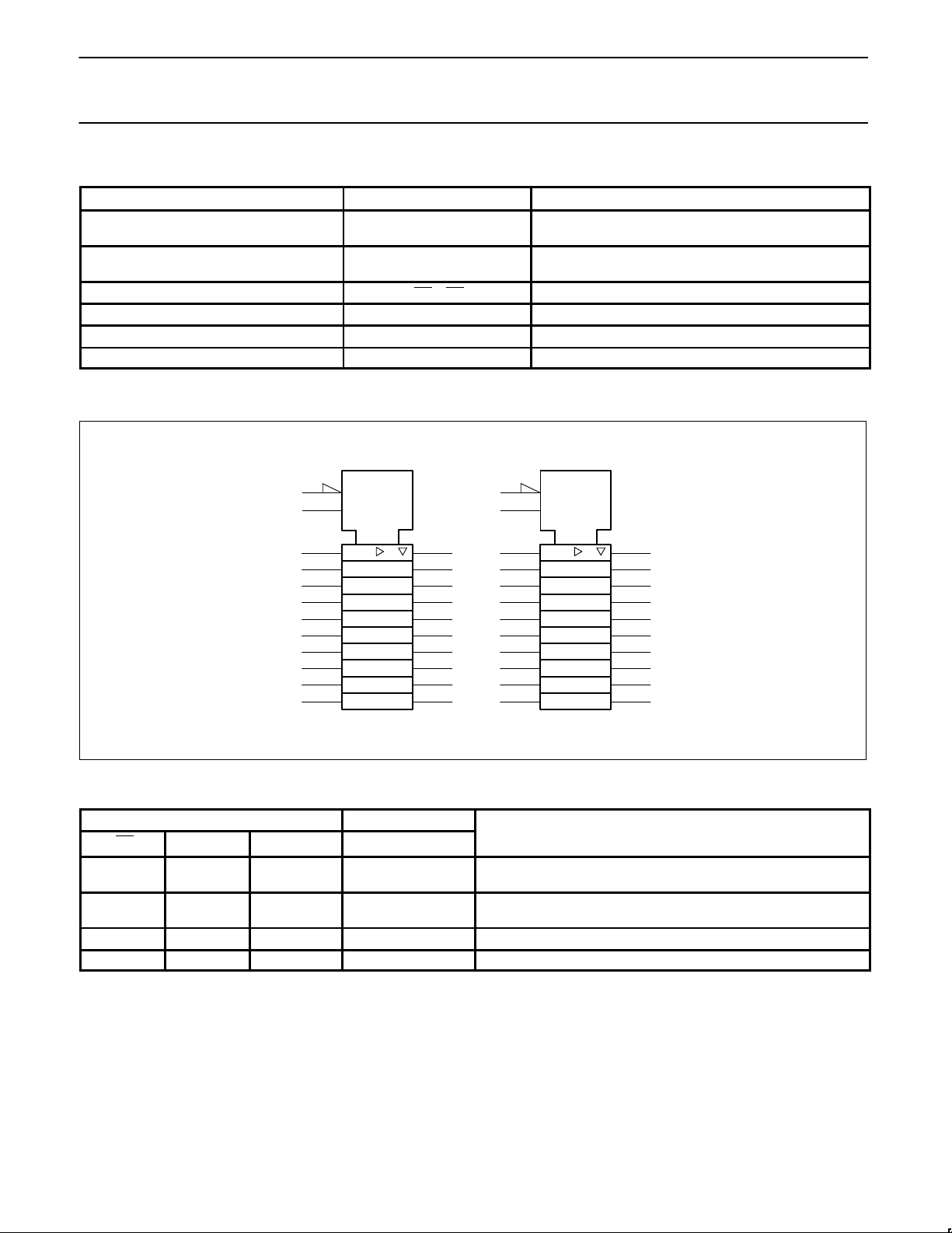
PIN DESCRIPTION
PIN NUMBER SYMBOL FUNCTION
45, 44, 42, 41, 39, 38, 37, 36, 35, 34,
33, 32, 31, 29, 28, 27, 25, 24, 23, 22
1D0 – 1D9
2D0 – 2D9
Data inputs
48, 49, 50, 51, 1, 2, 3, 5, 6, 7, 8, 9,
10, 11, 12, 13, 15, 16, 18, 19
1Q0 – 1Q9
2Q0 – 2Q9
Data outputs
47, 20 1OE, 2OE Output enable inputs (active-Low)
46, 21 1LE, 2LE Latch enable inputs (active rising edge)
4, 17, 30, 43 GND Ground (0V)
14, 26, 40, 52 V
CC
Positive supply voltage
LOGIC SYMBOL (IEEE/IEC)
C1
C1
45 48
44 49
42 50
41 51
39 1
38 2
37 3
36 5
1D
46
EN
47
35 6
34 7
33 8
32 9
31 10
29 11
28 12
27 13
25 15
24 16
1D
21
EN
20
23 18
22 19
FUNCTION TABLE
INPUTS OUTPUTS OPERATING MODE
nOE nLE nDx nQ0 – nQ9
L
L
H
H
L
H
L
H
Transparent
L
L
↓
↓
l
h
L
H
Latched
H X X Z High impedance
L L X NC Hold
H = High voltage level
h = High voltage level one set-up time prior to the High-to-Low LE transition
L = Low voltage level
l = Low voltage level one set-up time prior to the High-to-Low LE transition
↓ = High-to-Low LE transition
NC= No change
X = Don’t care
Z = High impedance “off” state
Page 3
Philips Semiconductors Advanced BiCMOS Products Product specification
MB2841Dual 10-bit bus interface latch (3-State)
August 24, 1993
3
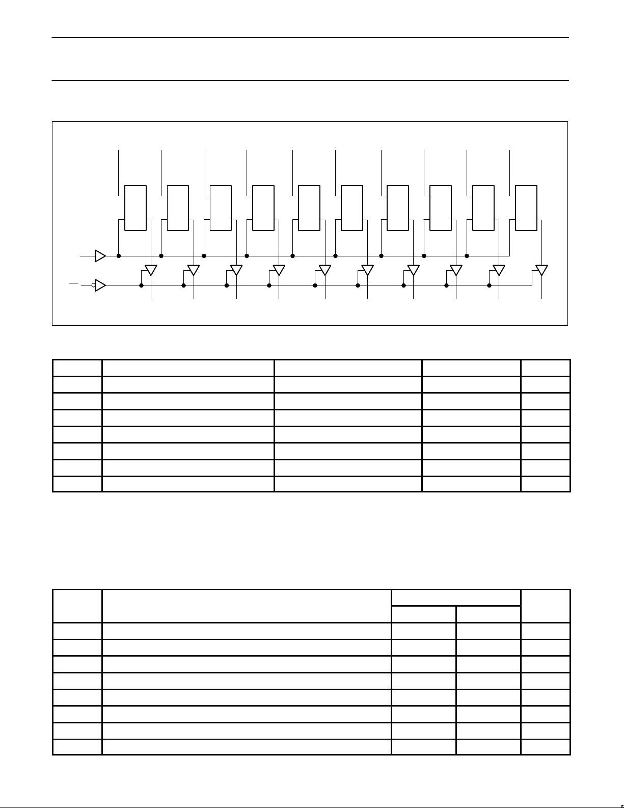
LOGIC DIAGRAM
L Q
D
nD0
nQ0
nLE
nOE
L Q
D
nD1
nQ1
L Q
D
nD2
nQ2
L Q
D
nD3
nQ3
L Q
D
nD4
nQ4
L Q
D
nD5
nQ5
L Q
D
nD6
nQ6
L Q
D
nD7
nQ7
L Q
D
nD8
nQ8
L Q
D
nD9
nQ9
ABSOLUTE MAXIMUM RATINGS
1, 2
SYMBOL
PARAMETER CONDITIONS RATING UNIT
V
CC
DC supply voltage –0.5 to +7.0 V
I
IK
DC input diode current VI < 0 –18 mA
V
I
DC input voltage
3
–1.2 to +7.0 V
I
OK
DC output diode current VO < 0 –50 mA
V
OUT
DC output voltage
3
output in Off or High state –0.5 to +5.5 V
I
OUT
DC output current output in Low state 128 mA
T
stg
Storage temperature range –65 to 150 °C
NOTES:
1. Stresses beyond those listed may cause permanent damage to the device. These are stress ratings only and functional operation of the
device at these or any other conditions beyond those indicated under “recommended operating conditions” is not implied. Exposure to
absolute-maximum-rated conditions for extended periods may affect device reliability.
2. The performance capability of a high-performance integrated circuit in conjunction with its thermal environment can create junction
temperatures which are detrimental to reliability. The maximum junction temperature of this integrated circuit should not exceed 150°C.
3. The input and output voltage ratings may be exceeded if the input and output current ratings are observed.
RECOMMENDED OPERATING CONDITIONS
SYMBOL PARAMETER LIMITS UNIT
Min Max
V
CC
DC supply voltage 4.5 5.5 V
V
I
Input voltage 0 V
CC
V
V
IH
High-level input voltage 2.0 V
V
IL
Low-level Input voltage 0.8 V
I
OH
High-level output current –32 mA
I
OL
Low-level output current 64 mA
∆t/∆v Input transition rise or fall rate 0 5 ns/V
T
amb
Operating free-air temperature range –40 +85 °C
Page 4
Philips Semiconductors Advanced BiCMOS Products Product specification
MB2841Dual 10-bit bus interface latch (3-State)
August 24, 1993
4
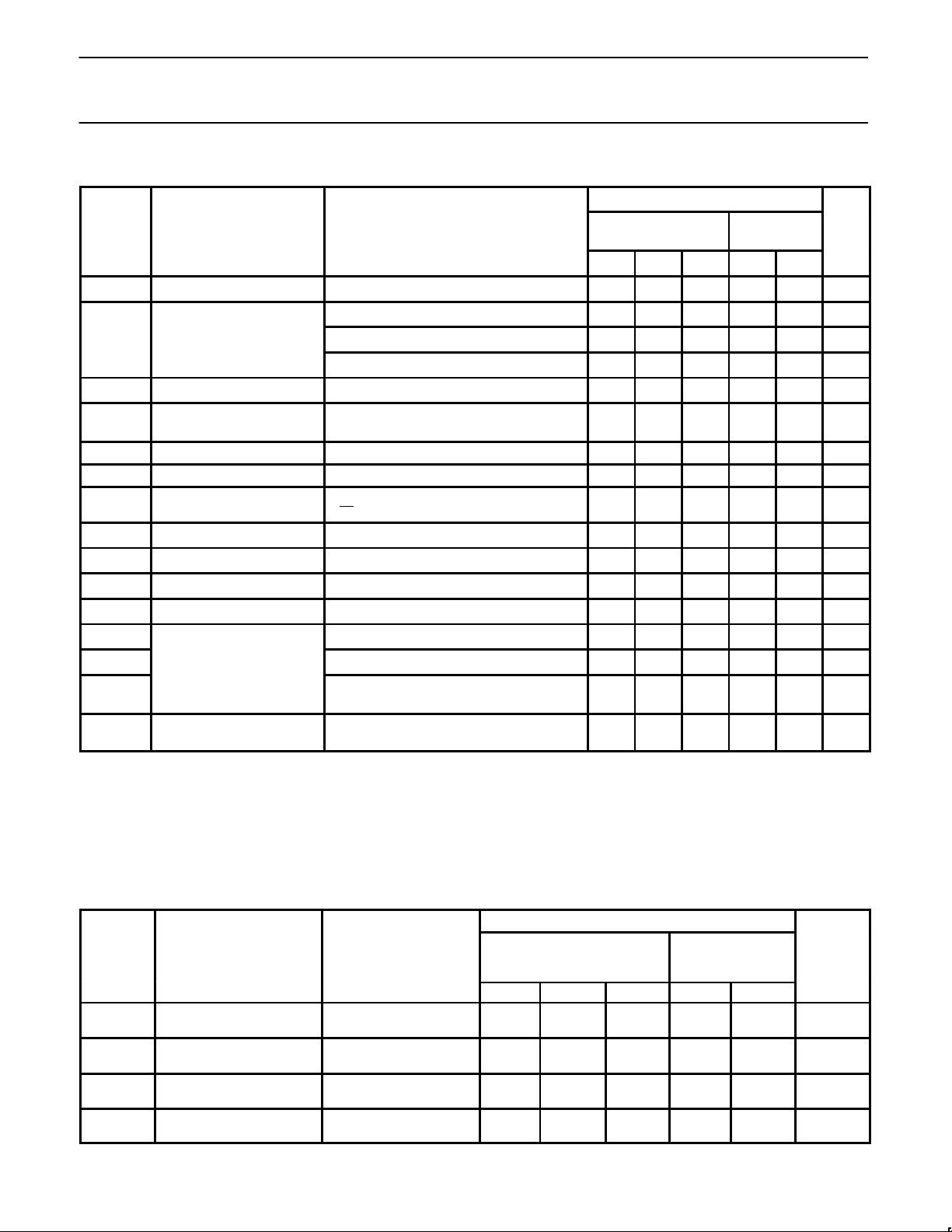
DC ELECTRICAL CHARACTERISTICS
LIMITS
SYMBOL PARAMETER TEST CONDITIONS T
amb
= +25°C
T
amb
= –40°C
to +85°C
UNIT
MIN TYP MAX MIN MAX
V
IK
Input clamp voltage VCC = 4.5V; IIK = –18mA –0.9 –1.2 –1.2 V
VCC = 4.5V; IOH = –3mA; VI = VIL or V
IH
2.5 2.9 2.5 V
V
OH
High-level output voltage VCC = 5.0V; IOH = –3mA; VI = VIL or V
IH
3.0 3.4 3.0 V
VCC = 4.5V; IOH = –32mA; VI = VIL or V
IH
2.0 2.4 2.0 V
V
OL
Low-level output voltage VCC = 4.5V; IOL = 64mA; VI = VIL or V
IH
0.42 0.55 0.55 V
V
RST
Power-up output
voltage
NO TAG
VCC = 5.5V; IO = 1mA; VI = GND or V
CC
0.13 0.55 0.55 V
I
I
Input leakage current VCC = 5.5V; VI = GND or 5.5V ±0.01 ±1.0 ±1.0 µA
I
OFF
Power-off leakage current VCC = 0.0V; VO or VI ≤ 4.5V ±5.0 ±100 ±100 µA
I
PU/PD
Power-up/down 3-State
output current
4
VCC = 2.1V; VO = 0.5V; VI = GND or VCC;
V
OE
= Don’t care
±5.0 ±50 ±50 µA
I
OZH
3-State output High current VCC = 5.5V; VO = 2.7V; VI = VIL or V
IH
5.0 50 50 µA
I
OZL
3-State output Low current VCC = 5.5V; VO = 0.5V; VI = VIL or V
IH
–5.0 –50 –50 µA
I
CEX
Output High leakage current VCC = 5.5V; VO = 5.5V; VI = GND or V
CC
5.0 50 50 µA
I
O
Output current
1
VCC = 5.5V; VO = 2.5V –50 –70 –180 –50 –180 mA
I
CCH
VCC = 5.5V; Outputs High, VI = GND or V
CC
120 250 250 µA
I
CCL
Quiescent supply current VCC = 5.5V; Outputs Low, VI = GND or V
CC
56 76 76 mA
I
CCZ
VCC = 5.5V; Outputs 3-State;
V
I
= GND or V
CC
120 250 250 µA
∆I
CC
Additional supply current per
input pin
2
VCC = 5.5V; one input at 3.4V,
other inputs at V
CC
or GND
0.5 1.5 1.5 mA
NOTES:
1. Not more than one output should be tested at a time, and the duration of the test should not exceed one second.
2. This is the increase in supply current for each input at 3.4V.
3. For valid test results, data must not be loaded into the flip-flops (or latches) after applying the power.
4. This parameter is valid for any V
CC
between 0V and 2.1V with a transition time of up to 10msec. From VCC = 2.1V to VCC = 5V ± 10% a
transition time of up to 100µsec is permitted.
AC CHARACTERISTICS
GND = 0V, tR = tF = 2.5ns, CL = 50pF, RL = 500Ω
LIMITS
SYMBOL PARAMETER WAVEFORM
T
amb
= +25oC
V
CC
= +5.0V
T
amb
= -40 to
+85
o
C
V
CC
= +5.0V ±0.5V
UNIT
MIN TYP MAX MIN MAX
t
PLH
t
PHL
Propagation delay
nDx to nQx
2
1.5
1.7
3.1
3.5
4.4
4.7
1.5
1.7
5.0
5.3
ns
t
PLH
t
PHL
Propagation delay
nLE to nQx
1
2.4
2.9
4.2
4.6
5.7
6.0
2.4
2.9
6.5
6.7
ns
t
PZH
t
PZL
Output enable time
to High and Low level
4
5
1.3
2.3
3.1
4.0
4.2
5.2
1.3
2.3
4.9
5.9
ns
t
PHZ
t
PLZ
Output disable time
from High and Low level
4
5
1.0
1.5
3.3
3.2
4.6
4.5
1.0
1.5
5.1
5.0
ns
Page 5
Philips Semiconductors Advanced BiCMOS Products Product specification
MB2841Dual 10-bit bus interface latch (3-State)
August 24, 1993
5
AC SETUP REQUIREMENTS
GND = 0V, tR = tF = 2.5ns, CL = 50pF, RL = 500Ω
LIMITS
SYMBOL PARAMETER WAVEFORM
T
amb
= +25oC
V
CC
= +5.0V
T
amb
= -40 to
+85
o
C
V
CC
= +5.0V ±0.5V
UNIT
Min Typ Max Min Max
ts(H)
t
s
(L)
Setup time, High or Low
nDx to nLE
3
2.0
1.5
0.8
0.4
2.0
1.5
ns
th(H)
t
h
(L)
Hold time, High or Low
nDx to nLE
3
0.5
0.5
–0.3
–0.7
0.5
0.5
ns
tw(H) nLE pulse width High 1 2.9 1.9 2.9 ns
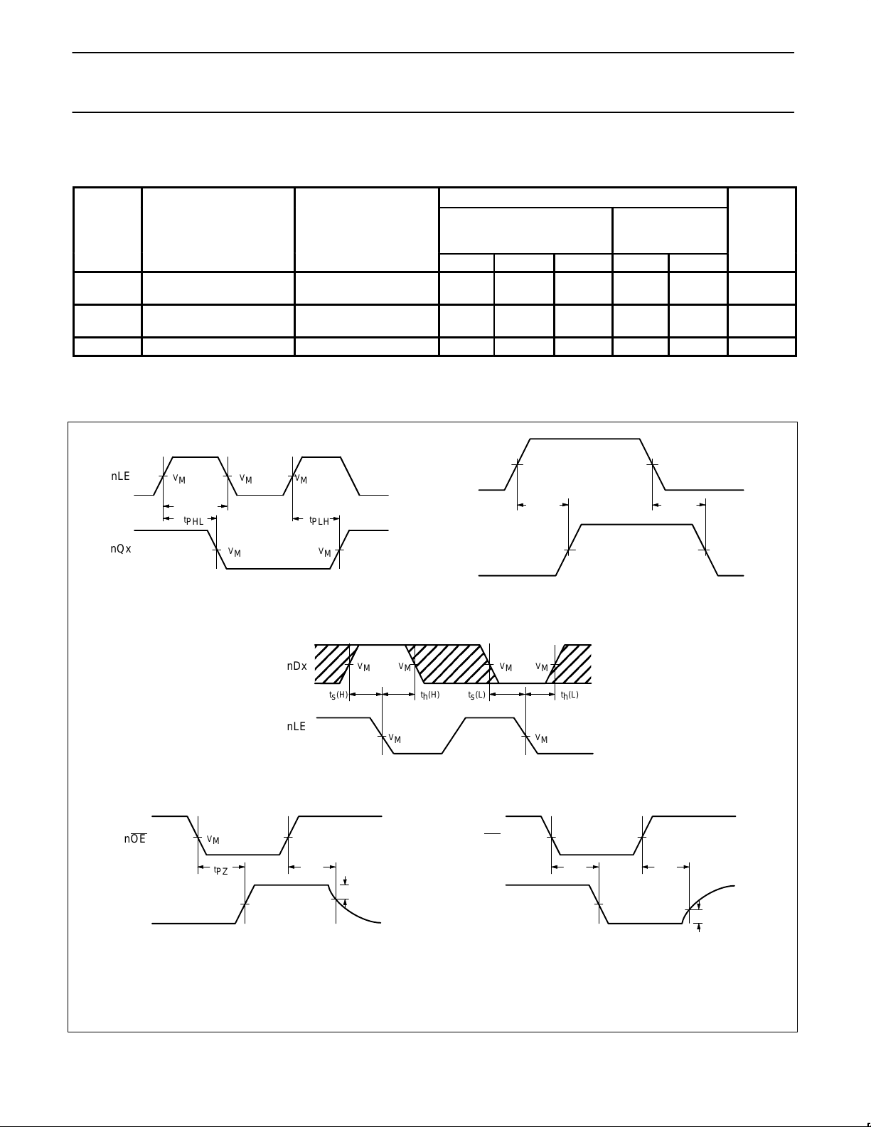
AC WAVEFORMS
VM = 1.5V, VIN = GND to 3.0V
tw(H)
V
M
V
M
V
M
V
M
V
M
t
PHL
t
PLH
nLE
nQx
V
M
nDx
V
M
V
M
V
M
V
MVM
nLE
ts(H) th(H) ts(L) th(L)
nOE
V
M
t
PZH
t
PHZ
0V
V
OH
–0.3V
nQx
nOE
t
PZL
t
PLZ
VOL +0.3V
nQx
V
M
V
M
V
M
V
M
V
M
NOTE: The shaded areas indicate when the input is permitted to change for predictable output performance.
nDx INPUT
V
M
V
M
nQx OUTPUT
V
M
V
M
t
PLH
t
PHL
Waveform 1. Propagation Delay, Latch Enable Input to
Output, and Enable Pulse Width
Waveform 2. Propagation Delay for Data to Outputs
Waveform 3. Data Setup and Hold Times
Waveform 4. 3–State Output Enable Time to High Level
and Output Disable Time from High Level
Waveform 5. 3–State Output Enable Time to Low Level
and Output Disable Time from Low Level
Page 6
Philips Semiconductors Advanced BiCMOS Products Product specification
MB2841Dual 10-bit bus interface latch (3-State)
August 24, 1993
6
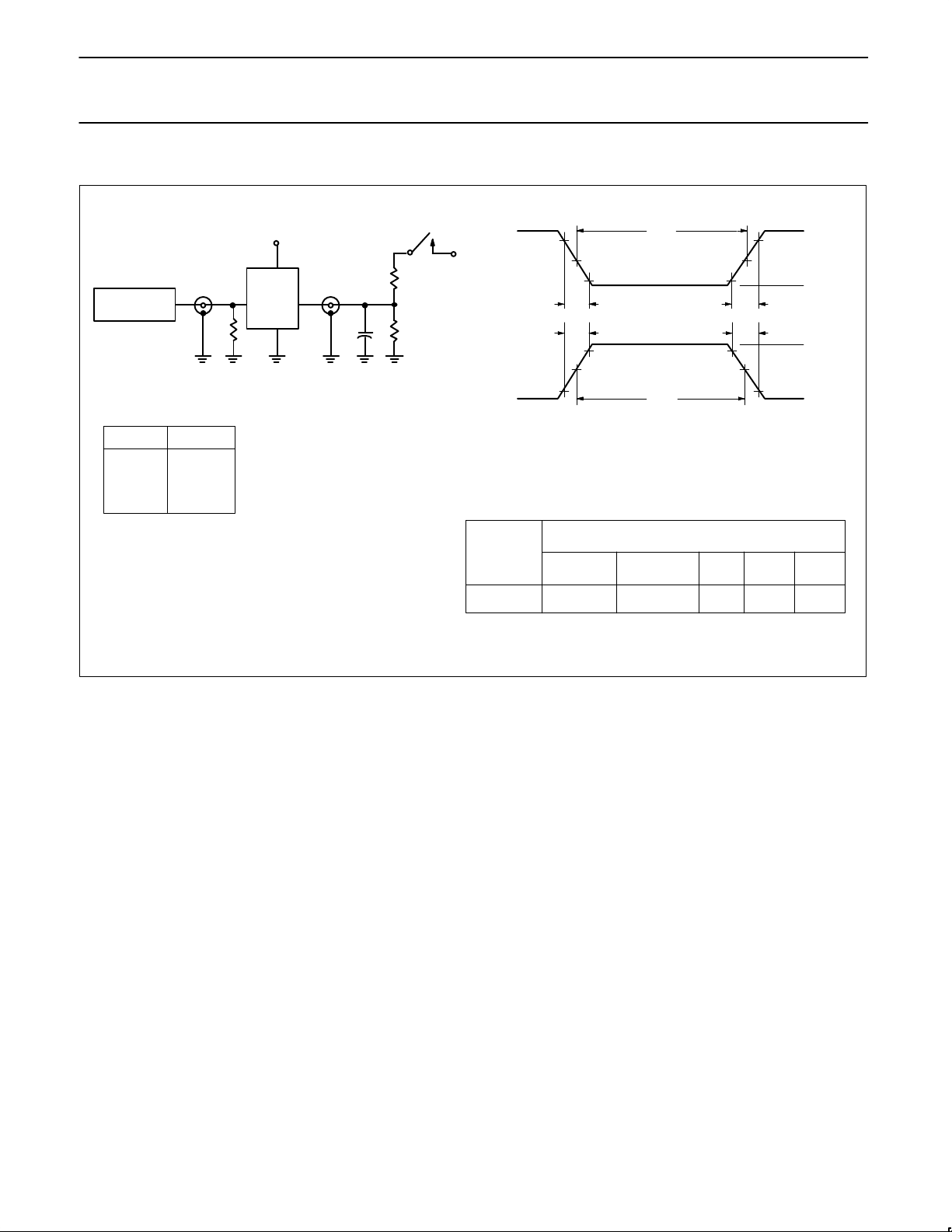
TEST CIRCUIT AND WAVEFORM
PULSE
GENERATOR
R
T
V
IN
D.U.T
V
OUT
C
L
R
L
V
CC
R
L
7.0V
Test Circuit for 3-State Outputs
V
M
V
M
t
W
AMP (V)
NEGATIVE
PULSE
10% 10%
90%
90%
0V
V
M
V
M
t
W
AMP (V)
POSITIVE
PULSE
90% 90%
10%
10%
0V
t
THL
(tF)
t
TLH
(tR) t
THL
(tF)
t
TLH
(tR)
VM = 1.5V
Input Pulse Definition
DEFINITIONS
RL = Load resistor; see AC CHARACTERISTICS for value.
C
L
= Load capacitance includes jig and probe capacitance;
see AC CHARACTERISTICS for value.
R
T
= Termination resistance should be equal to Z
OUT
of
pulse generators.
INPUT PULSE REQUIREMENTS
FAMILY
Amplitude Rep. Rate t
W
t
R
t
F
MB 3.0V 1MHz 500ns 2.5ns 2.5ns
SWITCH POSITION
TEST SWITCH
t
PLZ
closed
t
PZL
closed
All other open
Page 7
Philips Semiconductors Advanced BiCMOS Products Product specification
MB2841Dual 10-bit bus interface latch (3-State)
August 24, 1993
7
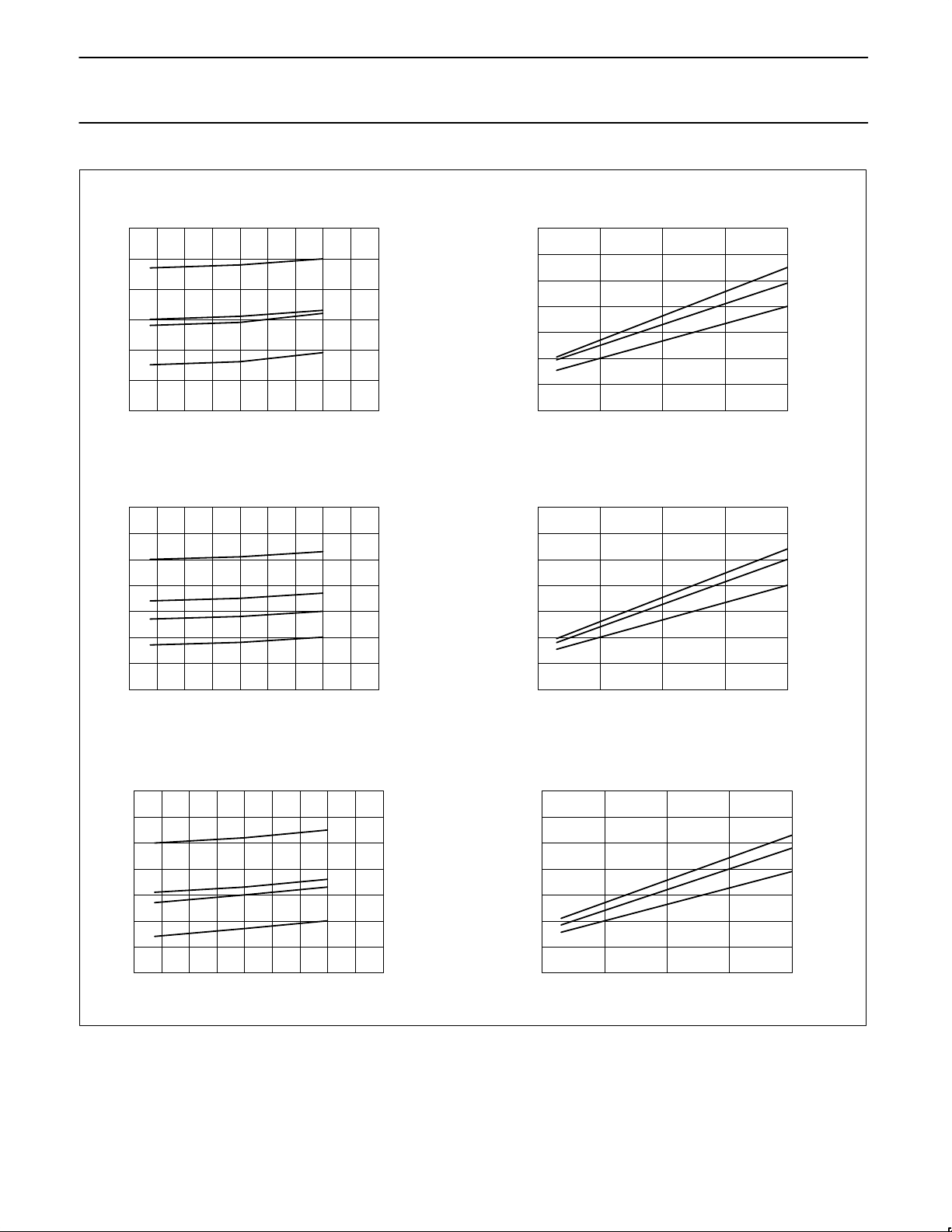
Adjustment of t
PHL
for
Load Capacitance and # of Outputs Switching
nDx to nQx
t
PLH
vs Temperature (T
amb
)
C
L
= 50pF, 1 Output Switching
nDx to nQx
°C
MAX
4.5V
CC
5.5V
CC
MIN
ns
Offset in ns
Adjustment of t
PLH
for
Load Capacitance and # of Outputs Switching
nDx to nQx
pF
20 switching
10 switching
1 switching
ns
Offset in ns
t
PHL
vs Temperature (T
amb
)
C
L
= 50pF, 1 Output Switching
nDx to nQx
°C
MAX
4.5V
CC
5.5V
CC
MIN
pF
20 switching
10 switching
1 switching
ns
Offset in ns
t
PLH
vs Temperature (T
amb
)
C
L
= 50pF, 1 Output Switching
nLE to nQx
°C
MAX
4.5V
CC
5.5V
CC
MIN
Adjustment of t
PLH
for
Load Capacitance and # of Outputs Switching
nLE to nQx
pF
20 switching
10 switching
1 switching
6
5
4
3
2
1
0
–55 –35 –15 5 25 45 65 85 105 125
7
6
5
4
3
2
1
0
–55 –35 –15 5 25 45 65 85 105 125
5
4
3
2
1
0
–1
–2
0 50 100 150 200
5
4
3
2
1
0
–1
–2
0 50 100 150 200
8
7
6
5
4
3
2
1
–55 –35 –15 5 25 45 65 85 105 125
5
4
3
2
1
0
–1
–2
0 50 100 150 200
Page 8
Philips Semiconductors Advanced BiCMOS Products Product specification
MB2841Dual 10-bit bus interface latch (3-State)
August 24, 1993
8
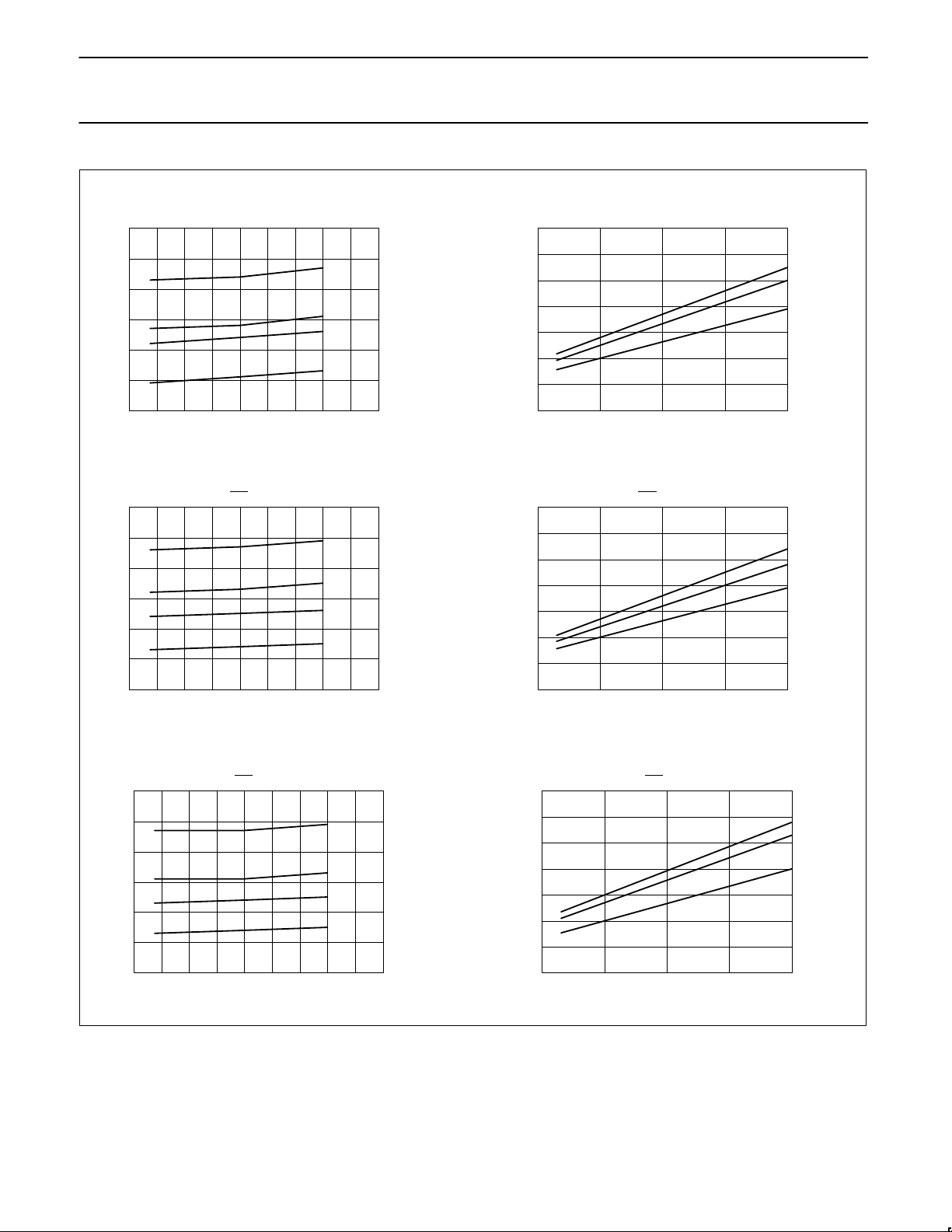
t
PHL
vs Temperature (T
amb
)
C
L
= 50pF, 1 Output Switching
nLE to nQx
°C
MAX
4.5V
CC
5.5V
CC
MIN
ns
Offset in ns
Adjustment of t
PHL
for
Load Capacitance and # of Outputs Switching
nLE to nQx
pF
20 switching
10 switching
1 switching
ns
Offset in ns
t
PZH
vs Temperature (T
amb
)
C
L
= 50pF, 1 Output Switching
nOE
to nQx
°C
MAX
4.5V
CC
5.5V
CC
MIN
Adjustment of t
PZH
for
Load Capacitance and # of Outputs Switching
nOE
to nQx
pF
20 switching
10 switching
1 switching
ns
Offset in ns
t
PZL
vs Temperature (T
amb
)
C
L
= 50pF, 1 Output Switching
nOE
to nQx
°C
MAX
4.5V
CC
5.5V
CC
MIN
Adjustment of t
PZL
for
Load Capacitance and # of Outputs Switching
nOE
to nQx
pF
20 switching
10 switching
1 switching
8
7
6
5
4
3
2
–55 –35 –15 5 25 45 65 85 105 125
6
5
4
3
2
1
0
–55 –35 –15 5 25 45 65 85 105 125
5
4
3
2
1
0
–1
–2
0 50 100 150 200
5
4
3
2
1
0
–1
–2
0 50 100 150 200
7
6
5
4
3
2
1
–55 –35 –15 5 25 45 65 85 105 125
5
4
3
2
1
0
–1
–2
0 50 100 150 200
Page 9
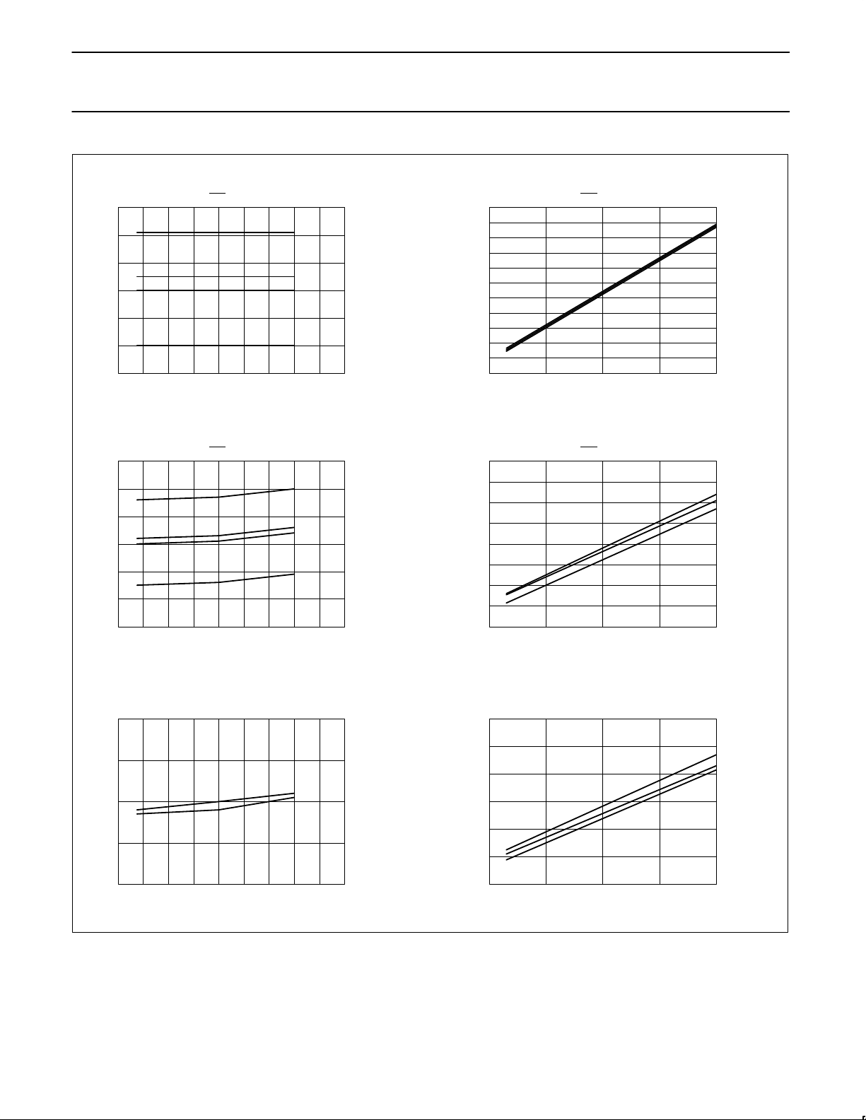
Philips Semiconductors Advanced BiCMOS Products Product specification
MB2841Dual 10-bit bus interface latch (3-State)
August 24, 1993
9
t
PHZ
vs Temperature (T
amb
)
C
L
= 50pF, 1 Output Switching
nOE
to nQx
°C
MAX
4.5V
CC
5.5V
CC
MIN
ns
Offset in ns
Adjustment of t
PHZ
for
Load Capacitance and # of Outputs Switching
nOE
to nQx
pF
20 switching
10 switching
1 switching
ns
Offset in ns
t
PLZ
vs Temperature (T
amb
)
C
L
= 50pF, 1 Output Switching
nOE
to nQx
°C
MAX
4.5V
CC
5.5V
CC
MIN
Adjustment of t
PLZ
for
Load Capacitance and # of Outputs Switching
nOE
to nQx
pF
20 switching
10 switching
1 switching
ns
Offset in ns
t
TLH
vs Temperature (T
amb
)
C
L
= 50pF, 1 Output Switching
°C
4.5V
CC
5.5V
CC
Adjustment of t
TLH
for
Load Capacitance and # of Outputs Switching
pF
20 switching
10 switching
1 switching
6
5
4
3
2
1
0
–55 –35 –15 5 25 45 65 85 105 125
6
5
4
3
2
1
0
–55 –35 –15 5 25 45 65 85 105 125
8
7
6
5
4
3
2
1
0
–1
–2
–3
0 50 100 150 200
6
5
4
3
2
1
0
–1
–2
0 50 100 150 200
4
3
2
1
0
–55 –35 –15 5 25 45 65 85 105 125
9
7
5
3
1
–1
–3
0 50 100 150 200
Page 10
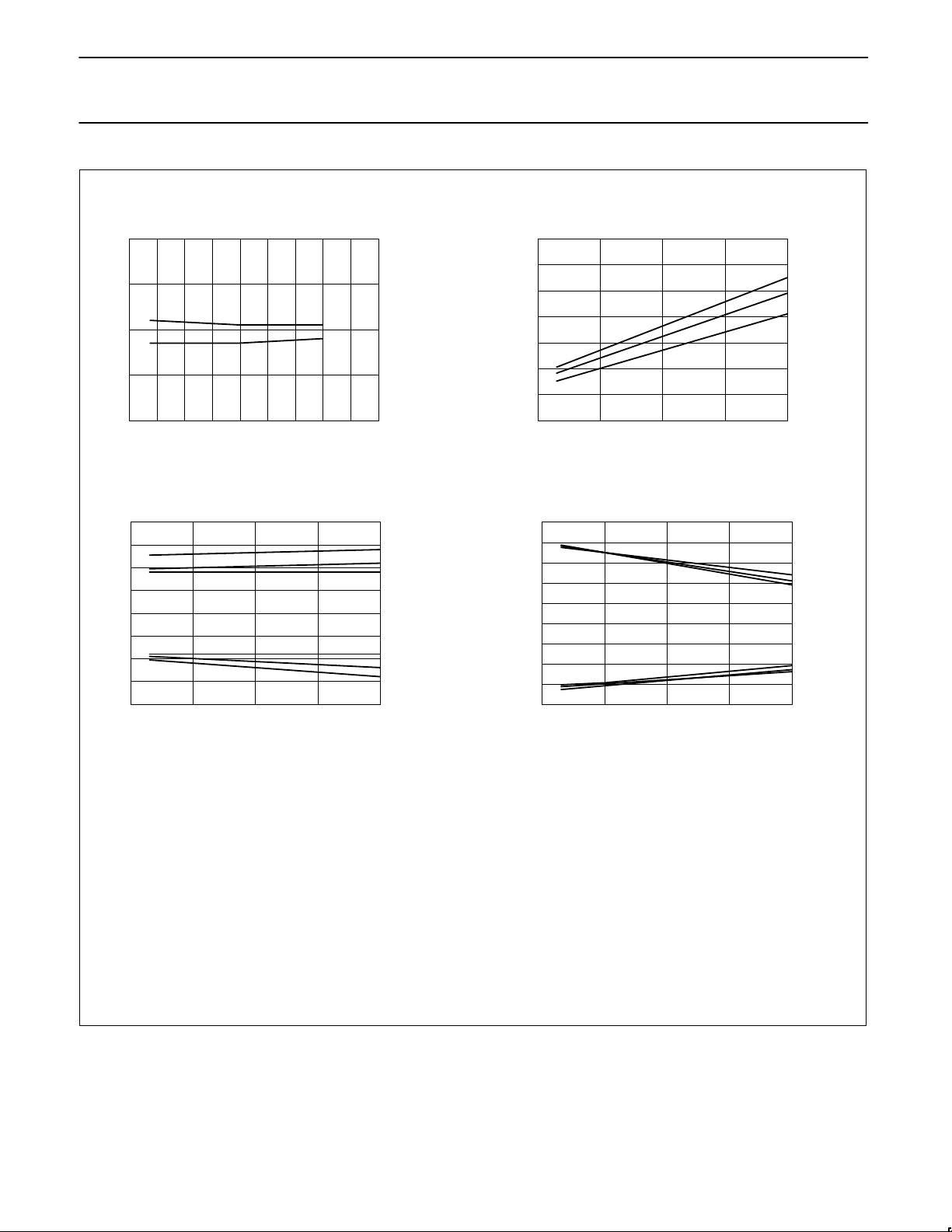
Philips Semiconductors Advanced BiCMOS Products Product specification
MB2841Dual 10-bit bus interface latch (3-State)
August 24, 1993
10
ns
Offset in ns
t
THL
vs Temperature (T
amb
)
C
L
= 50pF, 1 Output Switching
°C
4.5V
CC
5.5V
CC
Adjustment of t
THL
for
Load Capacitance and # of Outputs Switching
pF
20 switching
10 switching
1 switching
Volts
Volts
V
OHV
and V
OLP
vs Load Capacitance
V
CC
= 5V, VIN = 0 to 3V
pF
125°C
25°C
–55°C
V
OHP
and V
OLV
vs Load Capacitance
V
CC
= 5V, VIN = 0 to 3V
pF
125°C
25°C
–55°C
125°C
25°C
–55°C
125°C
25°C
–55°C
4
3
2
1
0
–55 –35 –15 5 25 45 65 85 105 125
4.0
3.5
3.0
2.5
2.0
1.5
1.0
0.5
0
0 50 100 150 200
5
4
3
2
1
0
–1
–2
0 50 100 150 200
6
5
4
3
2
1
0
–1
–2
–3
0 50 100 150 200
 Loading...