

Page 1

INTEGRATED CIRCUITS
MB2541
Dual octal buffer line driver (3-State)
Product specification
Supersedes data of 1993 Aug 18
IC23 Data Handbook
1998 Jan 16
Page 2
Philips Semiconductors Product specification
MB254116-bit buffer/line drivers (3-State)
FEA TURES
•Two 8-bit bus interfaces
•Power-up 3-State
•Multiple V
and GND pins minimize switching noise
CC
•Provides ideal interface and increases fan-out of MOS
Microprocessors
•3-State buffers sink 64mA and source 32mA
•Latch-up protection exceeds 500mA per Jedec Std 17
•ESD protection exceeds 2000 V per MIL STD 883 Method 3015
and 200 V per Machine Model
•Inputs are disabled during 3-State mode
QUICK REFERENCE DATA
SYMBOL PARAMETER
C
t
PLH
t
PHL
C
OUT
I
CCZ
IN
Propagation delay
nIx to nYx
CL = 50pF; VCC = 5V
Input capacitance VI = 0V or V
Output capacitance VO = 0V or VCC; 3-State 7 pF
Total supply current Outputs disabled; VCC =5.5V 65 µA
DESCRIPTION
The MB2541 high-performance BiCMOS device combines low
static and dynamic power dissipation with high speed and high
output drive.
The MB2541 has two 8-bit buffers that are ideal for driving bus lines.
The outputs are all capable of sinking 64mA and sourcing 32mA.
CONDITIONS
T
= 25°C; GND = 0V
amb
CC
TYPICAL UNIT
3.0
3.1
4 pF
ns
ORDERING INFORMATION
PACKAGES TEMPERATURE RANGE OUTSIDE NORTH AMERICA NORTH AMERICA DWG NUMBER
52–pin plastic Quad Flat Pack –40°C to +85°C MB2541 BB MB2541 BB SOT379-1
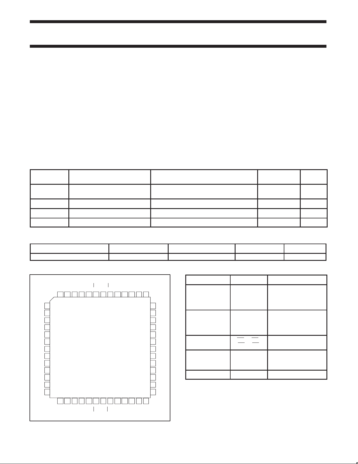
PIN CONFIGURATION
1Y3
1Y2
GND
1Y1
1
V
CC
2
1Y4
1Y5
3
GND
4
1Y6
5
1Y7
6
GND
7
2Y0
8
2Y1
9
GND
10
2Y2
11
2Y3
12
13
V
CC
2Y4
2Y5
2Y6
GND
1Y0
1OE0
GND
47 4446 434950 41 40425152 4548
52–pin PQFP
19 2220 231716 25 26241514 2118
2Y7
2OE0
GND
1OE1
2OE1
1A0
2A7
1A1
2A6
GND
GND
1A2
2A5
1A3
39
38
37
36
35
34
33
32
31
30
29
28
27
2A4
V
CC
1A4
1A5
GND
1A6
1A7
GND
2A0
2A1
GND
2A2
2A3
V
CC
SB00082
PIN DESCRIPTION
PIN NUMBER SYMBOL NAME AND FUNCTION
44, 43, 41, 40,
38, 37, 35, 34,
32, 31, 29, 28,
26, 25, 23, 22
48, 49, 51, 52,
2, 3, 5, 6,
8, 9, 11, 12,
14, 15, 17, 18
47, 45, 19, 21
4, 7, 10, 16,
20, 24, 30, 33,
36, 42, 46, 50
1, 13, 27, 39 V
1A0 – 1A7
2A0 – 2A7
1Y0 – 1Y7,
2Y0 – 2Y7
1OE0, 1OE1,
2OE0, 2OE1
Data inputs
Data outputs
Output enables
GND Ground (0V)
CC
Positive supply voltage
1998 Jan 16 853–1574 18869
2
Page 3
Philips Semiconductors Product specification
MB254116-bit buffer/line drivers (3-State)
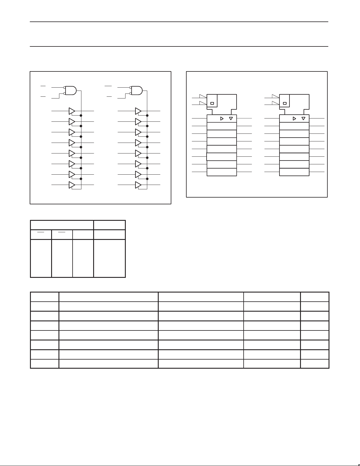
LOGIC SYMBOL
47
0
1OE
45
1
1OE
1A0
1A1
1A2
1A3
1A4
1A5
1A6
1A7
44
43
41
40
38
37
35
34
48
1Y0
49
1Y1
51
1Y2
52
1Y3
2
1Y4
3
1Y5
5
1Y6
6
1Y7
FUNCTION TABLE
INPUTS OUTPUTS
nOE0 nOE1 nIx nYx
L L L L
L L H H
X H X Z
H X X Z
2OE
2OE
0
1
2A0
2A1
2A2
2A3
2A4
2A5
2A6
2A7
LOGIC SYMBOL (IEEE/IEC)
19
21
32
31
29
28
26
25
23
22
8
2Y0
9
2Y1
11
2Y2
12
2Y3
14
2Y4
15
2Y5
17
2Y6
18
2Y7
SB00083
47
45
44
43
41
40
38
37
35
34
&
EN
48
49
51
52
19
&
21
32
31
29
28
26
2
25
3
23
5
22
6
EN
8
9
11
12
14
15
17
18
SB00084
ABSOLUTE MAXIMUM RA TINGS
SYMBOL
V
CC
I
IK
V
I
I
OK
V
OUT
I
OUT
T
stg
DC supply voltage –0.5 to +7.0 V
DC input diode current VI < 0 –18 mA
DC input voltage
DC output diode current VO < 0 –50 mA
DC output voltage
DC output current output in Low state 128 mA
Storage temperature range –65 to 150 °C
PARAMETER CONDITIONS RATING UNIT
3
3
1, 2
–1.2 to +7.0 V
output in Off or High state –0.5 to +5.5 V
NOTES:
1. Stresses beyond those listed may cause permanent damage to the device. These are stress ratings only and functional operation of the
device at these or any other conditions beyond those indicated under “recommended operating conditions” is not implied. Exposure to
absolute-maximum-rated conditions for extended periods may affect device reliability .
2. The performance capability of a high-performance integrated circuit in conjunction with its thermal environment can create junction
temperatures which are detrimental to reliability. The maximum junction temperature of this integrated circuit should not exceed 150°C.
3. The input and output voltage ratings may be exceeded if the input and output current ratings are observed.
1998 Jan 16
3
Page 4
Philips Semiconductors Product specification
MB254116-bit buffer/line drivers (3-State)
RECOMMENDED OPERATING CONDITIONS
SYMBOL PARAMETER LIMITS UNIT
Min Max
V
CC
V
V
V
I
OH
I
OL
∆t/∆v Input transition rise or fall rate 0 10 ns/V
T
amb
DC ELECTRICAL CHARACTERISTICS
SYMBOL PARAMETER TEST CONDITIONS T
V
IK
V
OH
V
OL
I
I
OFF
IPU/I
I
OZH
I
OZL
I
CEX
I
O
I
CCH
I
CCL
I
CCZ
∆I
CC
NOTES:
1. Not more than one output should be tested at a time, and the duration of the test should not exceed one second.
2. This is the increase in supply current for each input at 3.4V.
DC supply voltage 4.5 5.5 V
Input voltage 0 V
I
High-level input voltage 2.0 V
IH
Low-level Input voltage 0.8 V
IL
CC
High-level output current –32 mA
Low-level output current 64 mA
Operating free-air temperature range –40 +85 °C
LIMITS
T
amb
= +25°C
amb
to +85°C
Min Typ Max Min Max
Input clamp voltage VCC = 4.5V; IIK = –18mA –0.9 –1.2 –1.2 V
VCC = 4.5V; IOH = –3mA; VI = VIL or V
High-level output voltage VCC = 5.0V; IOH = –3mA; VI = VIL or V
VCC = 4.5V; IOH = –32mA; VI = VIL or V
Low-level output voltage VCC = 4.5V; IOL = 64mA; VI = VIL or V
Input leakage current VCC = 5.5V; VI = GND or 5.5V ±0.01 ±1.0 ±1.0 µA
I
IH
IH
IH
IH
2.5 2.9 2.5 V
3.0 3.4 3.0 V
2.0 2.4 2.0 V
0.42 0.55 0.55 V
Power-off leakage current VCC = 0.0V; VO or VI ≤ 4.5V ±5.0 ±100 ±100 µA
Power-up/down 3-State
PD
output current
3-State output High current VCC = 5.5V; VO = 2.7V; VI = VIL or V
3-State output Low current VCC = 5.5V; VO = 0.5V; VI = VIL or V
Output high leakage current VCC = 5.5V; VO = 5.5V; VI = GND or V
Output current
1
Quiescent supply current VCC = 5.5V; Outputs Low, VI = GND or V
Additional supply current per
input pin
2
VCC = 2.0V; VO = 0.5V; VI = GND or VCC;
VOE = V
CC
IH
IH
CC
±5.0 ±50 ±50 µA
5.0 50 50 µA
–5.0 –50 –50 µA
5.0 50 50 µA
VCC = 5.5V; VO = 2.5V –50 –70 –180 –50 –180 mA
VCC = 5.5V; Outputs High, VI = GND or V
VCC = 5.5V; Outputs 3-State;
VI = GND or V
CC
Outputs enabled, one input at 3.4V , other
inputs at VCC or GND; VCC = 5.5V
CC
CC
65 250 250 µA
48 60 60 mA
65 250 250 µA
0.5 1.5 1.5 mA
= –40°C
V
UNIT
1998 Jan 16
4
Page 5

Philips Semiconductors Product specification
MB254116-bit buffer/line drivers (3-State)
AC CHARACTERISTICS
GND = 0V; tR = tF = 2.5ns; CL = 50pF, RL = 500Ω
LIMITS
T
SYMBOL PARAMETER WAVEFORM
t
PLH
t
PHL
t
PZH
t
PZL
t
PHZ
t
PLZ
Propagation delay
nIx to nYx
Output enable time
to High and Low level
Output disable time
from High and Low level
1
2
2
AC WAVEFORMS
VM = 1.5V, VIN = GND to 3.0V
= +25°C
amb
VCC = +5.0V
Min Typ Max Min Max
1.2
1.2
1.3
2.1
1.8
1.7
3.0
3.1
3.6
4.7
4.3
4.0
4.5
4.5
5.2
6.1
6.2
5.4
T
= –40°C to +85°C
amb
VCC = +5.0V ±0.5V
1.2
1.2
1.3
2.1
1.8
1.7
5.1
5.1
5.8
7.1
6.8
5.9
UNIT
ns
ns
ns
nIx INPUT
nYx OUTPUT
V
M
t
PLH
V
M
V
M
t
PHL
V
M
SB00085
Waveform 1. W aveforms Showing the Input (An) to Output (Yn)
Propagation Delays
nOEn INPUT
nYx OUTPUT
nYx OUTPUT
V
M
t
PZL
V
M
t
PZH
V
M
V
M
t
PLZ
t
PHZ
3.5V
V
OL
V
OL
V
OH
V
OH
0V
SB00086
+ 0.3V
– 0.3V
Waveform 2. Waveforms Showing the 3-State Output Enable
and Disable Times
1998 Jan 16
5
Page 6

Philips Semiconductors Product specification
MB254116-bit buffer/line drivers (3-State)
TEST CIRCUIT AND WAVEFORMS
V
CC
V
OUT
C
L
PULSE
GENERATOR
V
IN
D.U.T.
R
T
Test Circuit for 3-State Outputs
SWITCH POSITION
TEST SWITCH
t
PLZ
t
PZL
closed
closed
All other open
DEFINITIONS
= Load resistor; see AC CHARACTERISTICS for value.
R
L
C
= Load capacitance includes jig and probe capacitance; see AC
L
CHARACTERISTICS for value.
= Termination resistance should be equal to Z
R
T
of pulse generators.
OUT
t
90%
7.0V
NEGATIVE
R
L
PULSE
V
M
10% 10%
t
R
L
POSITIVE
PULSE
t
90% 90%
V
M
10%
W
V
M
(tF)
THL
(tR)t
TLH
V
M
t
W
= 1.5V
V
M
Input Pulse Definition
90%
10%
AMP (V)
0V
t
(tR)
TLH
(tF)
THL
AMP (V)
0V
INPUT PULSE REQUIREMENTS
FAMILY
Amplitude Rep. Rate t
t
W
t
R
F
MB 3.0V 1MHz 500ns 2.5ns 2.5ns
SB00010
1998 Jan 16
6
Page 7

Philips Semiconductors Product specification
MB254116-bit buffer/line drivers (3-State)
t
vs T emperature (T
PLH
= 50pF, 1 Output Switching
C
L
nIx to nYx
6
amb
)
Load Capacitance and # of Outputs Switching
Adjustment of t
nIx to nYx
PLH
for
4
5
4
3
ns
2
1
0
–55 –35 –15 5 25 45 65 85 105 125
°C
t
vs T emperature (T
PHL
= 50pF, 1 Output Switching
C
L
nIx to nYx
amb
)
7
6
5
4
ns
3
2
1
0
–55 –35 –15 5 25 45 65 85 105 125
°C
MAn
4.5V
5.5V
MIN
MAn
4.5V
5.5V
MIN
3
CC
CC
2
1
Offset in ns
0
16 switching
8 switching
1 switching
–1
–2
0 50 100 150 200
pF
Load Capacitance and # of Outputs Switching
Adjustment of t
nIx to nYx
PHL
for
4
3
2
CC
CC
1
Offset in ns
0
16 switching
8 switching
1 switching
–1
–2
0 50 100 150 200
pF
t
vs T emperature (T
PZH
C
= 50pF, 1 Output Switching
L
nOE
n to nYx
amb
)
7
6
5
4
ns
3
2
1
0
–55 –35 –15 5 25 45 65 85 105 125
°C
MAn
4.5V
5.5V
MIN
Load Capacitance and # of Outputs Switching
Adjustment of t
nOE
n to nYx
PZH
for
5
4
3
CC
CC
2
1
Offset in ns
16 switching
8 switching
1 switching
0
–1
–2
0 50 100 150 200
pF
SB00087
1998 Jan 16
7
Page 8

Philips Semiconductors Product specification
MB254116-bit buffer/line drivers (3-State)
t
vs T emperature (T
PZL
= 50pF, 1 Output Switching
C
L
nOE
n to nYx
8
7
6
5
ns
4
3
2
1
–55 –35 –15 5 25 45 65 85 105 125
°C
t
vs T emperature (T
PHZ
= 50pF, 1 Output Switching
C
L
nOE
n to nYx
8
7
6
5
4
ns
3
2
1
0
–55 –35 –15 5 25 45 65 85 105 125
°C
amb
amb
)
Load Capacitance and # of Outputs Switching
Adjustment of t
n to nYx
nOE
PZL
for
4
MAn
4.5V
5.5V
3
CC
CC
2
1
Offset in ns
0
16 switching
8 switching
1 switching
MIN
–1
–2
0 50 100 150 200
pF
)
Load Capacitance and # of Outputs Switching
Adjustment of t
n to nYx
nOE
PHZ
for
6
MAn
4.5V
5.5V
MIN
5
4
CC
CC
3
2
Offset in ns
1
0
16 switching
8 switching
1 switching
–1
–2
0 50 100 150 200
pF
t
vs T emperature (T
PLZ
C
= 50pF, 1 Output Switching
L
nOE
n to nYx
amb
)
7
6
5
4
ns
3
2
1
0
–55 –35 –15 5 25 45 65 85 105 125
°C
MAn
4.5V
5.5V
MIN
n to nYx
PLZ
for
Load Capacitance and # of Outputs Switching
Adjustment of t
nOE
6
5
4
CC
CC
3
16 switching
8 switching
1 switching
2
Offset in ns
1
0
–1
–2
0 50 100 150 200
pF
SB00088
1998 Jan 16
8
Page 9

Philips Semiconductors Product specification
MB254116-bit buffer/line drivers (3-State)
t
vs T emperature (T
TLH
= 50pF, 1 Output Switching
C
L
4
3
ns
2
1
–55 –35 –15 5 25 45 65 85 105 125
°C
t
vs T emperature (T
THL
= 50pF, 1 Output Switching
C
L
3.0
2.5
2.0
ns
1.5
1
–55 –35 –15 5 25 45 65 85 105 125
°C
amb
amb
)
Load Capacitance and # of Outputs Switching
Adjustment of t
TLH
for
9
4.5V
5.5V
8
7
6
CC
CC
5
4
3
2
Offset in ns
1
16 switching
8 switching
1 switching
0
–1
–2
–3
0 50 100 150 200
pF
)
Load Capacitance and # of Outputs Switching
Adjustment of t
THL
for
5
4
16 switching
8 switching
1 switching
4.5V
5.5V
3
CC
CC
2
1
Offset in ns
0
–1
–2
0 50 100 150 200
pF
and V
V
OHV
vs Load Capacitance
OLP
= 5V, VIN = 0 to 3V
V
CC
4.0
3.5
3.0
2.5
2.0
1.5
volts
1.0
0.5
0.0
–0.5
–1
0 50 100 150 200
pF pF
125°C
25°C
–55°C
125°C
25°C
–55°C
V
and V
OHP
vs Load Capacitance
OLV
= 5V, VIN = 0 to 3V
V
CC
6
5
4
3
2
volts
1
0
–1
–2
0 50 100 150 200
125°C
25°C
–55°C
125°C
25°C
–55°C
SB00089
1998 Jan 16
9
Page 10

Philips Semiconductors Product specification
Dual octal buffer line driver (3-State)
QFP52: plastic quad flat package; 52 leads (lead length 1.6 mm); body 10 x 10 x 2.0 mm SOT379-1
MB2541
1998 Jan 16
10
Page 11

Philips Semiconductors Product specification
Dual octal buffer line driver (3-State)
MB2541
NOTES
1998 Jan 16
11
Page 12

Philips Semiconductors Product specification
Dual octal buffer line driver (3-State)
Data sheet status
Data sheet
status
Objective
specification
Preliminary
specification
Product
specification
Product
status
Development
Qualification
Production
Definition
This data sheet contains the design target or goal specifications for product development.
Specification may change in any manner without notice.
This data sheet contains preliminary data, and supplementary data will be published at a later date.
Philips Semiconductors reserves the right to make chages at any time without notice in order to
improve design and supply the best possible product.
This data sheet contains final specifications. Philips Semiconductors reserves the right to make
changes at any time without notice in order to improve design and supply the best possible product.
[1]
MB2541
[1] Please consult the most recently issued datasheet before initiating or completing a design.
Definitions
Short-form specification — The data in a short-form specification is extracted from a full data sheet with the same type number and title. For
detailed information see the relevant data sheet or data handbook.
Limiting values definition — Limiting values given are in accordance with the Absolute Maximum Rating System (IEC 134). Stress above one
or more of the limiting values may cause permanent damage to the device. These are stress ratings only and operation of the device at these or
at any other conditions above those given in the Characteristics sections of the specification is not implied. Exposure to limiting values for extended
periods may affect device reliability.
Application information — Applications that are described herein for any of these products are for illustrative purposes only. Philips
Semiconductors make no representation or warranty that such applications will be suitable for the specified use without further testing or
modification.
Disclaimers
Life support — These products are not designed for use in life support appliances, devices or systems where malfunction of these products can
reasonably be expected to result in personal injury . Philips Semiconductors customers using or selling these products for use in such applications
do so at their own risk and agree to fully indemnify Philips Semiconductors for any damages resulting from such application.
Right to make changes — Philips Semiconductors reserves the right to make changes, without notice, in the products, including circuits, standard
cells, and/or software, described or contained herein in order to improve design and/or performance. Philips Semiconductors assumes no
responsibility or liability for the use of any of these products, conveys no license or title under any patent, copyright, or mask work right to these
products, and makes no representations or warranties that these products are free from patent, copyright, or mask work right infringement, unless
otherwise specified.
Philips Semiconductors
811 East Arques Avenue
P.O. Box 3409
Sunnyvale, California 94088–3409
Telephone 800-234-7381
Copyright Philips Electronics North America Corporation 1998
All rights reserved. Printed in U.S.A.
print code Date of release: 05-96
Document order number: 9397-750-03512
1998 Jan 16
12
 Loading...