

Page 1

FUJITSU SEMICONDUCTOR
DATA SHEET
DS04-21309-2E
ASSP
Serial Input PLL Frequency
Synthesizer
MB1511
■
DESCRIPTION
The Fujitsu MB1511 is a singl e chip serial input PLL frequenc y synthesizer designed for VHF tuner and cellular
telephone applications.
It contains a 1.1 GHz dual modulus prescaler which enables pulse swallow function, and an analog switch to speed
up lock up time.
It operates supply voltage of 3.0 V typ. and dissipates 7 mA typ. of current realized through the use of Fujitsu's unique
U-ESBIC Bi-CMOS technology.
The MB1511 is housed in SSOP package, this enables high integration.
■
FEATURES
• Low power supply voltage: VCC = 2.7 to 5.5 V
• High operating frequency: f
• Pulse swallow function: 64/65 or 128/129
• Low supply current: I
• Serial input 18-bit programmable divider consisting of:
Binary 7-bit swallow counter: 0 to 127
Binary 11-bit programmable counter: 16 to 2047
• Serial input 15-bit programmable reference divider consisting of:
Binary 14-bit programmable reference counter: 8 to 16383
1-bit switch counter (SW) sets divide ratio of prescaler
■
PACKAGE
CC
IN MAX
= 1.1 GHz (V
= 7 mA typ.
IN MIN
= –10dBm)
20 pin, Plastic SSOP
(Continued)
(FPT-20P-M03)
1
Page 2
MB1511
(Continued)
• On-chip analog switch achieves fast lock up time
• 2 types of phase detector output
On-chip charge pump (Bipolar type)
Output for external charge pump
• Wide operating temperature: –40°C to +85°C
• 20-pin Pl astic Shrink Small Outline Package (Suffix: –PFV)
■
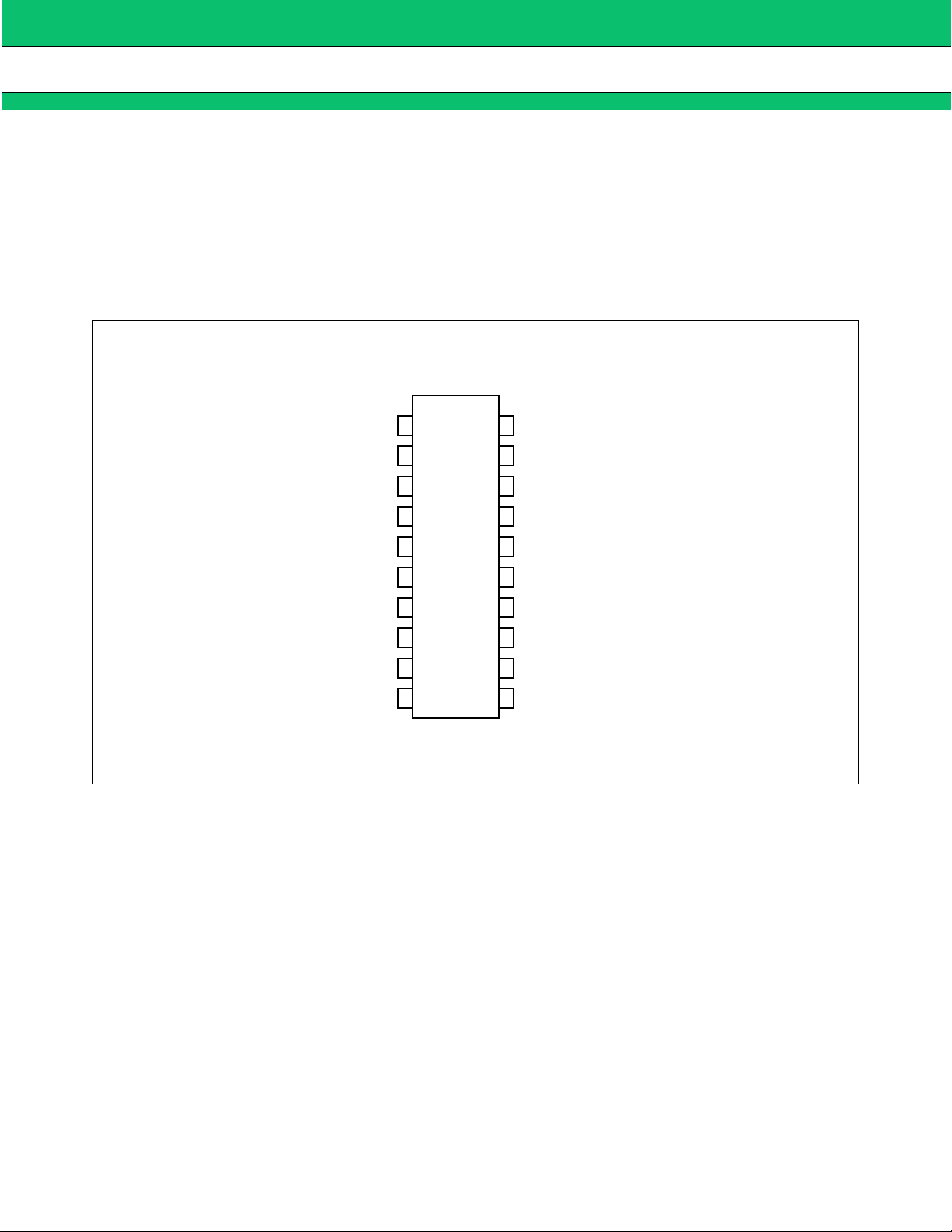
PIN ASSIGNMENT
(TOP VIEW)
1 φR20OSC
IN
2 NC19NC
CC
O
3 φP18OSC
4 fout17
5 BiSW16V
6 FC15D
7 LE14GND
8 Data13LD
9 NC12NC
10 Clock11fin
OUT
V P
(FPT-20P-M03)
2
Page 3
■
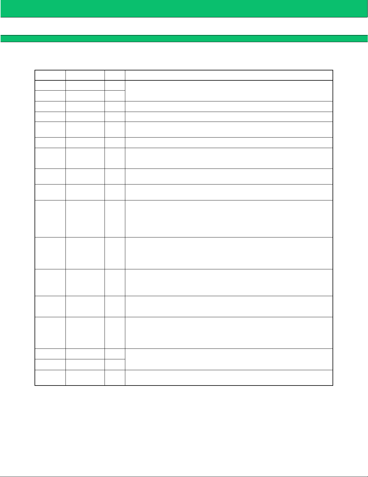
PIN DESCRIPTION
Pin No. Pin Name I/O Functions
1OSC
IN
I Oscillator input.
Oscillator output.
CC
P
O
OUT
O
A crystal is placed between OSC
IN
and OSC
— Power supply input for charge pump and analog switch.
— Power supply voltage input.
Charge pump output.
O
The characteristics of charge pump is reversed depending upon FC input.
3OSC
4V
5V
6D
7 GND — Ground.
OUT
MB1511
.
8LDO
Normally this pin outputs high level. While the phase difference of f
exists, this pin outputs low level.
Phase comparator output.
10 f
IN
11 Clock I
Prescaler input.
I
The connection with an external VCO should be AC connection.
Clock input for 19-bit shift register and 16-bit shift register.
On rising edge of the clock shifts one bit of data into the shift registers.
Binary serial data input.
The last bit of the data is a control bit which specified destination of shift reg-
13 Data I
isters.
When this bit is high level and LE is high level, the data stored in shift register is transferred to 15-bit latch. When this bit is low level and LE is high
level, the data is transferred to 18-bit latch.
Load enable input (with internal pull up resistor).
When LE is high or open, the data stored in shift register is transferred into
14 LE I
latch depending upon the control bit. At the time, internal charge pump output is connected to BISW pin because internal analog switch becomes ON
state.
Phase select input of phase comparator (with internal pull up resistor).
15 FC I
When FC is lo w lev el, the char acteristic s of charge pump , phas e compara tor
is reversed.
FC input signal controls f
Analog switch output.
16 BISW O
Usually BISW pin is set high-impedance state. When internal analog switch
is ON (LE pin is high level), this pin outputs internal charge pump output.
Minitor pin of phase comparator input.
out
pin outputs either programmable reference divider output (fr) or program-
17 f
OUT
f
mable divider ou tput (f
O
FC = H: It is the same as f
FC = L: It is the same as f
out
pin (test pin) output level, fr or fp.
p
) depending upon FC pin input level.
r
output level.
p
output level.
r
and fp
18 φP O Output for external charge pump.
The characteristics are reversed according to FC input.
20 φRO
2, 9
12, 19
NC — No connection.
φP pin is N-channel open drain output.
3
Page 4
MB1511
■
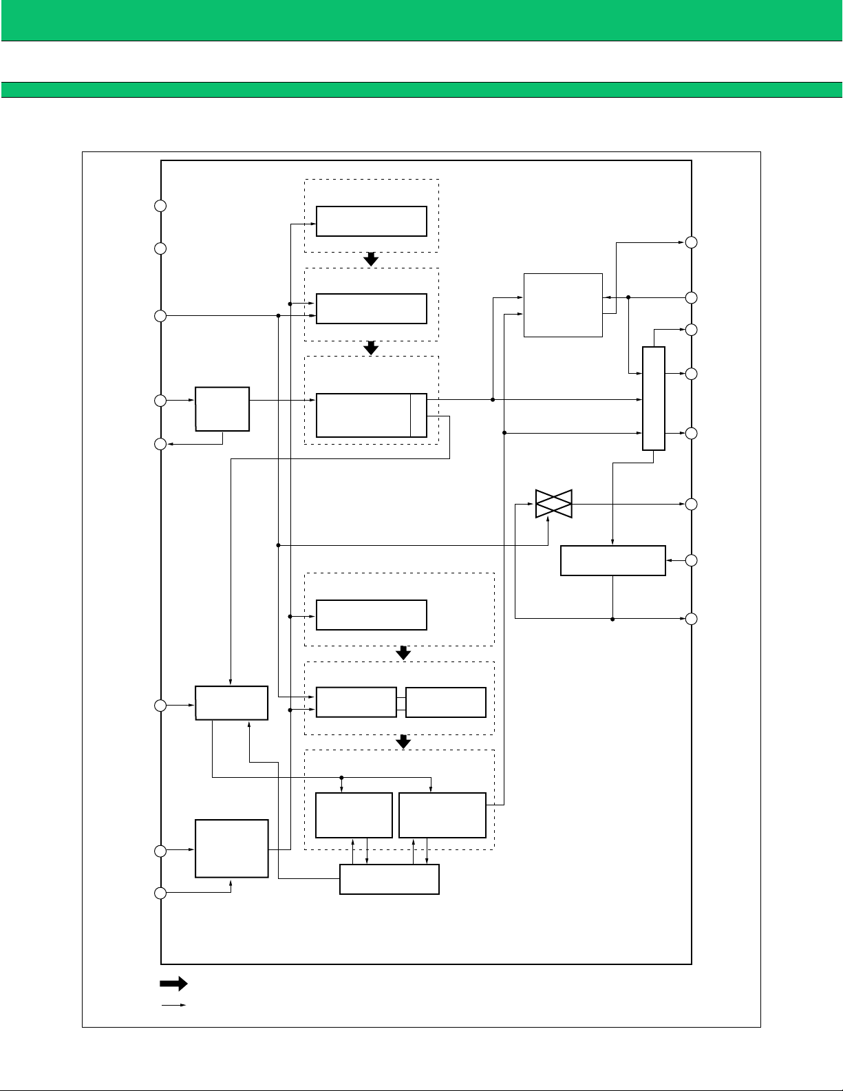
BLOCK DIAGRAM
V
CC
GND
LE
OSC IN
OSC OUT
5
16 bit shift register
16 bit shift register
17
f
7
15 bit latch
14
15 bit latch
Monitor
frequency
changing
circuit
Programmable
reference divider
1
3
Cristal
oscillator
Binary 14-bit
reference counter
S
W
fr
fp
Phase comparator
OUT
15
FC
8
LD
20
φR
18
φP
Analog switch
16
BISW
Charge pump
4
P
V
19 bit shift register
Data
Clock
19 bit shift register
6
D O
18 bit latch
10
fIN
Prescaler
7 bit latch
11 bit latch
Programmable
Binary 7 bit
swallow
counter
13
Control
1 bit latch
Binary 11 bit
programmable
counter
Control circuit
11
: Data signal
: Control signal
4
Page 5

MB1511
■
FUNCTION AL DESCRIPTIONS
1. Pulse Swallow Function
The divide ratio is set using the following equation.
VCO
f
= [(M × N) + A] × f
VCO
: Output frequency of external voltage controlled oscillator (VCO)
f
M : Preset modulus of external dual modulus prescaler (64 or 128)
N : Preset divide ratio of binary 11-bit programmable counter (16 to 2047)
A : Preset divide ratio of binary 7-bit swallow counter (0 ≤ A ≤ 127, A < N)
OSC
f
: Output frequency of the external reference frequency oscillator
R : Preset divide ratio of binary 14-bit programmable reference counter (8 to 16383)
2. Serial Data Input
Serial data input is achieved by three inputs, such as Data pin, Clock pin and LE pin. Serial data input controls 15bit programmable reference divider and 18-bit programmable divider, respectively.
Binary serial data is input to Data pin.
On rising edge of clock shifts one bit of serial data into the internal shift registers and when load enable pin is high
level or open, stored data is transferred into latch depending upon the control bit.
Control data "H" data is transferred into 15-bit latch.
OSC
÷ R
Control data "L" data is transferred into 18-bit latch.
5
Page 6
MB1511
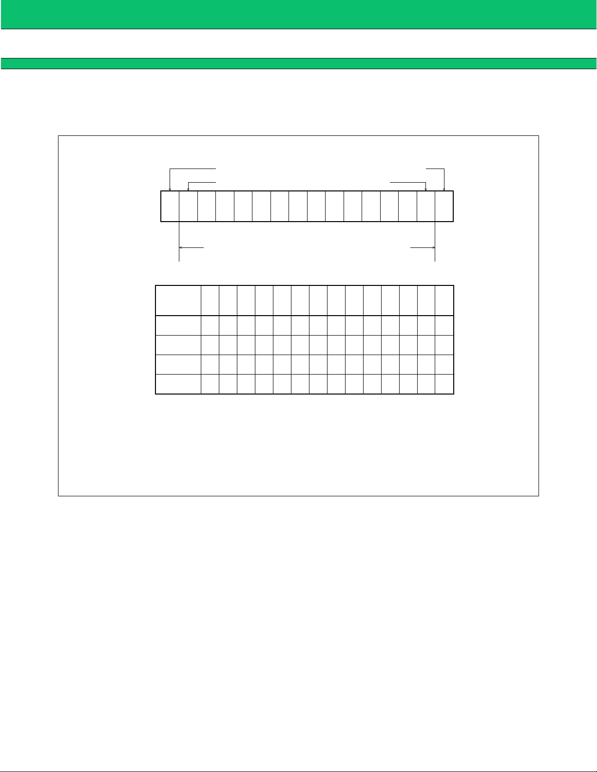
(1) Programmable Reference Divider
Programmable reference divider consists of 16-bit s hift register, 15-bit latch and 14-bit reference counter. Serial
16-bit data format is shown below.
Control bit
LSB
CS1S2S3S4S5S6S7S8S9S10S11S12S13S14S
Divide ratio of programmable reference counter setting bit
• 14-BIT PROGRAMMABLE REFERENCE COUNTER DIVIDE RATIO
Divide Ratio
R
8
9
16383
NOTES:
S14S13S12S11S10S9S8S7S6S5S4S3S2S
00000000001000
00000000001001
…
…
…
…
…
11111111111111
Divide ratio less than 8 is prohibited.
Divide ratio: 8 to 16383
SW: This bit selects divide ratio of prescaler.
SW = H: 64/65
SW = L: 128/129
S1 to S14: These bits select divide ratio of programmable reference divider.
C: Control bit (sets as high level).
Data is input from MSB side.
Divide ratio of prescaler setting bit
…
…
…
…
…
MSB
…
…
W
1
…
…
…
6
Page 7
MB1511
(2) Programmable Divider
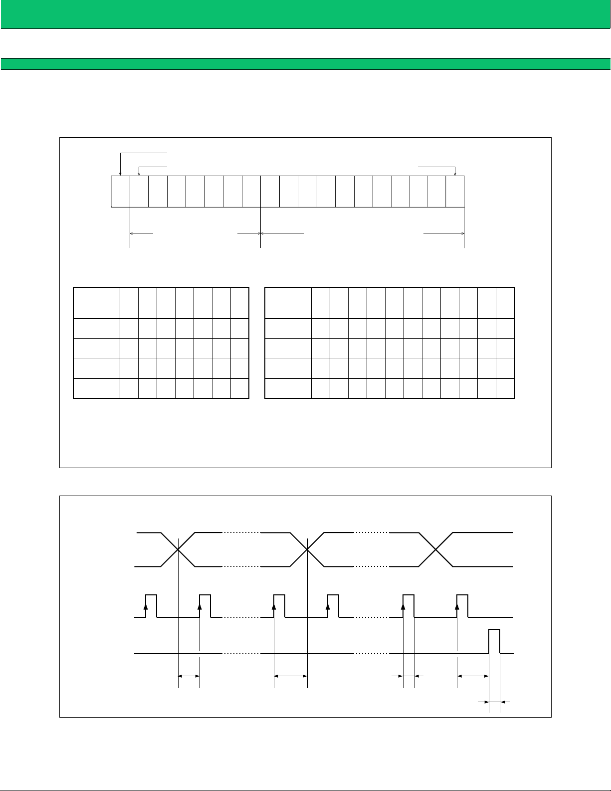
Programmable divider consists of 19-bit shift register, 18-bit latch, 7-bit swallow counter and 11-bit programmable
counter. Serial 19-bit data format is shown following page.
Control bit
LSB
CS1S2S3S4S5S6S7S8S9S10S11S12S13S
MSB
S15S16S17S
14
18
Divide ratio of swallow
counter setting bit
• 7-bit Swallow Counter Divide Ratio
Divide Ratio
A
0
1
127
S7S6S5S4S3S2S
0000000
0000001
…
…
…
…
1111111
3. Serial Data Input Timing
t 1~t
5
≤ 1 µs
Divide ratio of programmable
counter setting bit
• 11-bit Programmable Counter Divide Ratio
Divide Ratio
1
…
…
…
…
N
16
17
2047
Notes:Note: Divide ratio: 0 to 127
S18S17S16S15S14S13S12S11S10S9S
8
00000010001
00000010001
…
…
…
…
…
…
…
…
…
…
…
…
11111111111
Divide ratio less than 16 is prohibited.
Divide ratio: 16 to 2047
S1 to S7: Swallow counter divide ratio setting bit. (0 to 127)
S8 to S18: Programmable counter divide ratio setting bit. (16 to 2047)
C: Control bit (sets as low level).
Data is input from MSB side.
Data
S18 = MSB S17 S10 S9 S1 = LSB C : CONTROL BIT
Clock
LE
t
t
1
2
t
3
Notes:Paranthesis data is used for setting divide ratio of programmable reference divider.
On rising edge of clock shifts one bit of data in the shift register.
(C : CONTROL BIT)(S14)* (SW) (S8) (S7) (S1)
t
4
t
5
7
Page 8
MB1511
4. Phase Characteristics
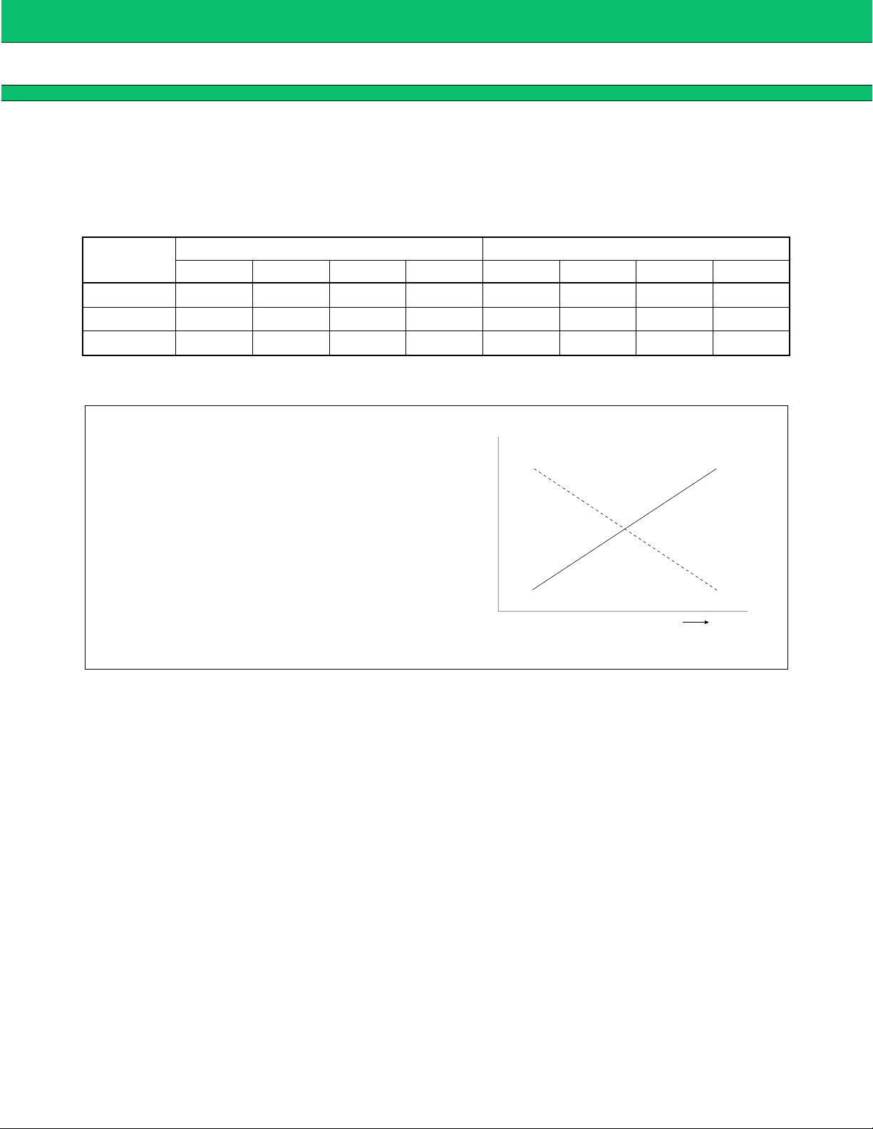
FC pin is provided to change pha se characteristics of phase c om parato r. Characteristics of internal charge pu mp
output level (D
monitor pin (f
O
(D
, φR, φP) and FC input level are shown below.
fr > fp H L L (fr) L H Z (fp)
fr = fp Z L Z (fr) Z L Z (fp)
fr < fp L H Z (fr) H L L (fp)
Note: Z = (High impedance)
Depending upon VCO characteristics, FC pin should be set accordingly:
O
), phase com parator output l evel (φR, φP) are reversed depending upon FC pin i nput level. Also,
OUT
) output level of phase comparator is controlled by FC pin input level. The relation between outputs
FC : “H” or open FC : “L”
φ
D
O
R
φ
Pf
OUT
φ
D
O
R
φ
Pf
OUT
(1)
• When VCO characteri stics are like (1) , FC
should be set High or open circuit; When
VCO characteristics are like (2), FC should
be set Low.
VCO Output Frequency
VCO Input Voltage
(2)
8
Page 9
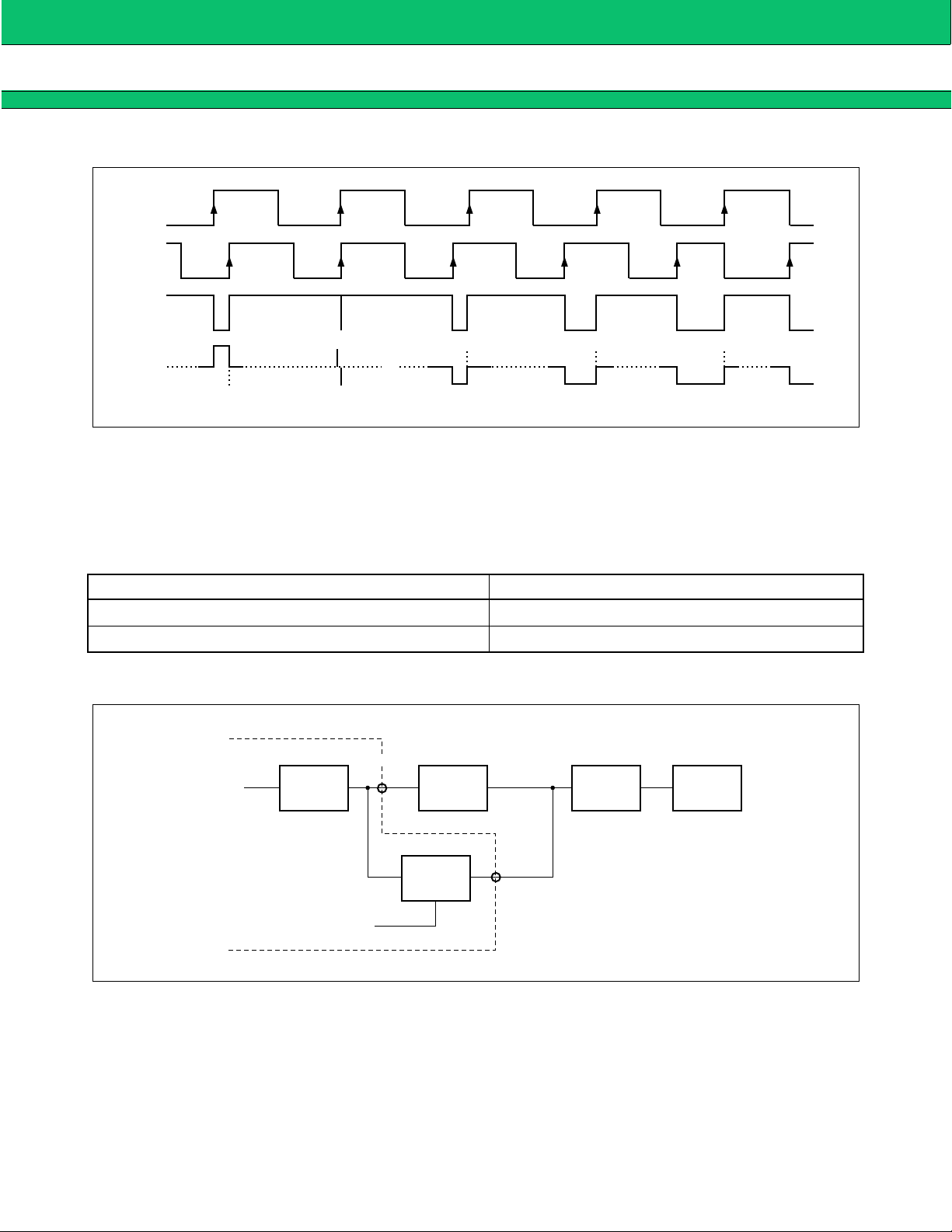
Phase comparator output waveforms are shown below.
fr
fp
LD
H
D
O
fr > fp
fr = fp fr < fp fr < fp fr < fp
Z
MB1511
L
Notes: Phase difference detection range: –2π to +2
Spike appearance depends on charge pump characteristics. Also, the spike is output in order to diminish dead band.
When fr>fp or fr<fp, spike might not appear depending upon charge rump characteristics.
π
5. Analog Switch
ON/OFF of analog switch is co ntrolled by LE input sig nal. When the anal og switch is ON, inter nal charge pu mp
output (D
O
) is connected to BISW pin. When the analog switch is OFF, BISW pin is set to high-impedance state.
LE Analog Switch
H (Changing the divide ratio of internal prescaler) ON
L (Normal operationg mode) OFF
When an analog switch is inser ted between LP1 and LP2, faster lock up times is achieved to reduce LPF time
constant during PLL channal switching.
D
O
CHARGE
PUMP
LPF-1 LPF-2 VCO
BISW
ANALOG
SW
(CONTROL SIGNAL LE)
9
Page 10
MB1511
■
ABSOLUTE MAXIMUM RATINGS (See WARNING)
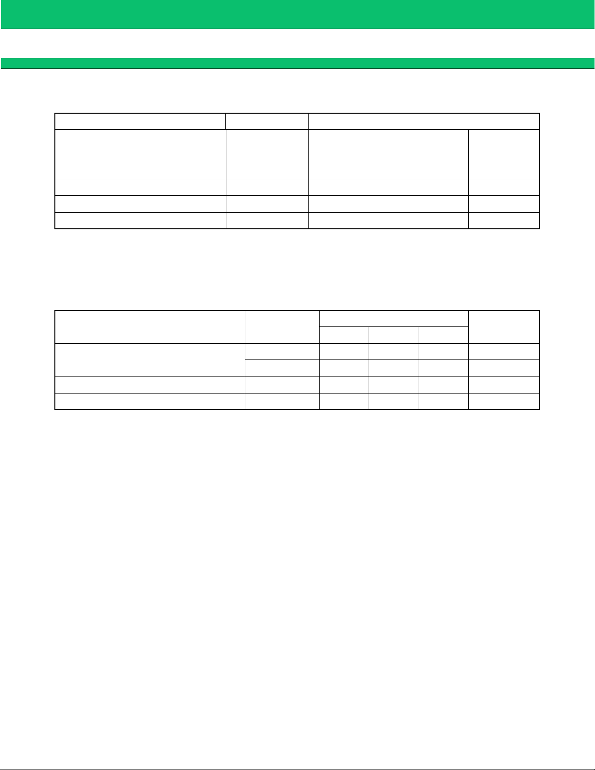
Parameter Symbol Rating Unit
CC
Power supply voltage
Output voltage V
Open-drain voltage V
Output current I
Storage temperature T
V
V
OUT
OOP
OUT
STG
P
–0.5 to 7.0 V
VCC to 10.0 V
–0.5 to VCC +0.5 V
–0.5 to 8.0 V
±10 mA
–55 to +125 °C
WARNING:
Permanent device damage may occur if the above
Absolute Maximum Ratings
are exceeded.
Functional operation sh ould be restri cted to the condition s as detailed in the operationa l sections of
this data sheet. Exposure to absolute maximum rating conditions for extended periods may affect device
reliability.
■
RECOMMENDED OPERATING CONDITIONS
Value
Parameter Symbol
Unit
Min. Typ. Max.
CC
V
2.7 3.0 5.5 V
Power supply voltage
Input voltage V
Operating temperature T
P
V
IN
a
CC
V
GND — V
—8.0 V
CC
–40 — +85 °C
V
HANDLING PRECAUTIONS
• This device should be transported and stored in anti-static containers.
• This is static-se nsitive dev ice; take proper anti -ESD preca utions. E nsure that per sonnel a nd equipme nt are
properly grounded. Cover workbenches with grounded conductive mats.
• Always turn the power supply off before inserting or removing the device from its socket.
• Protect leads with a conductive sheet when handing or transporting PC boards with devices.
10
Page 11
■
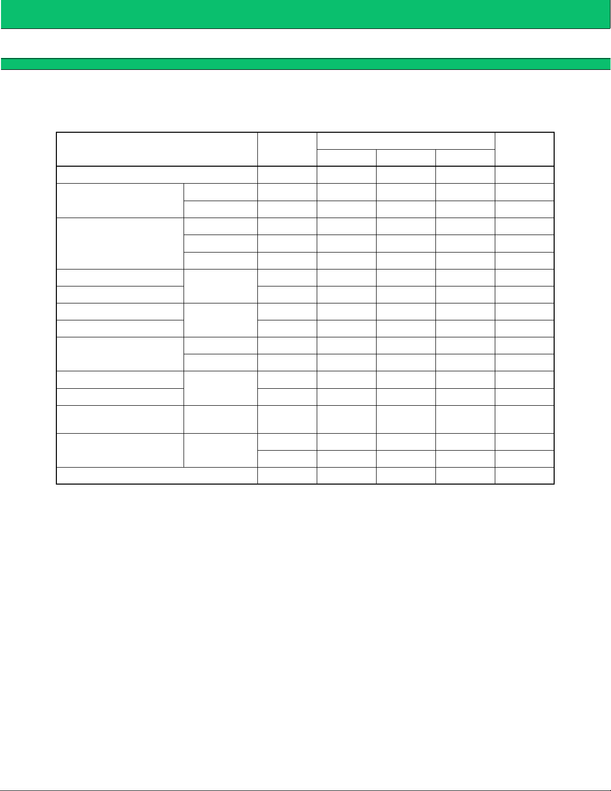
ELECTRICAL CHARACTERINSTICS
MB1511
(VCC = 2.7 V to 5.5 V, Ta = –40°C to +85°C)
Parameter Symbol
Power supply current*
1
2
fin*
Operating frequency
IN
OSC
3
fin-1*
Input sensitivity
High-level input voltage
Low-level input voltage V
4
fin-2*
IN
OSC
Except fin and
IN
OSC
f
V
V
V
High-level input current
Data clock
Low-level input current I
OSC
IN
I
Input current
LE, FC I
High-level output current
Low-level output current V
N-channel open drain
cutoff current
Output current
Except D
and OSC
O
D
Except D
and OSC
, φP*
O
OUT
6
O
OUT
VOH*
I
Analog switch on resistance R
CC
I
f
OSC
OSC
V
I
OSC
OFF
OH
I
I
IN
IH
LE
OL
fin1
fin2
IH
IL
IL
OL
ON
Values
Unit
Min. Typ. Max.
—7.0—mA
10 — 1100 MHz
—1220MHz
–4 — 6 dBm
–10 — 6 dBm
0.5 — — V
p-p
VCC×0.7 — — V
——V
CC
×0.3 V
—1.0—µA
— –1.0 — µA
—±50— µA
—–60—µA
5
2.2 — — V
——0.4V
——1.1µA
–1.0 — — mA
1.0 — — mA
—50—Ω
Notes: *1 fin =1.1 GHz, OSC
*2 AC coupling. Minimum operating frequency is measured when a capacitor 1000pF.
CC
*3 V
*4 V
*5 V
*6 V
=4.0 to 5.5V, 50 Ω
CC
=2.7 to 4.0V, 50 Ω
CC
=3V
P=VCC
to 8V, V
OOP
IN
=12 MHz, VCC=3V. Inputs are grounded and outputs are open.
=GND to 8V
11
Page 12
MB1511
■
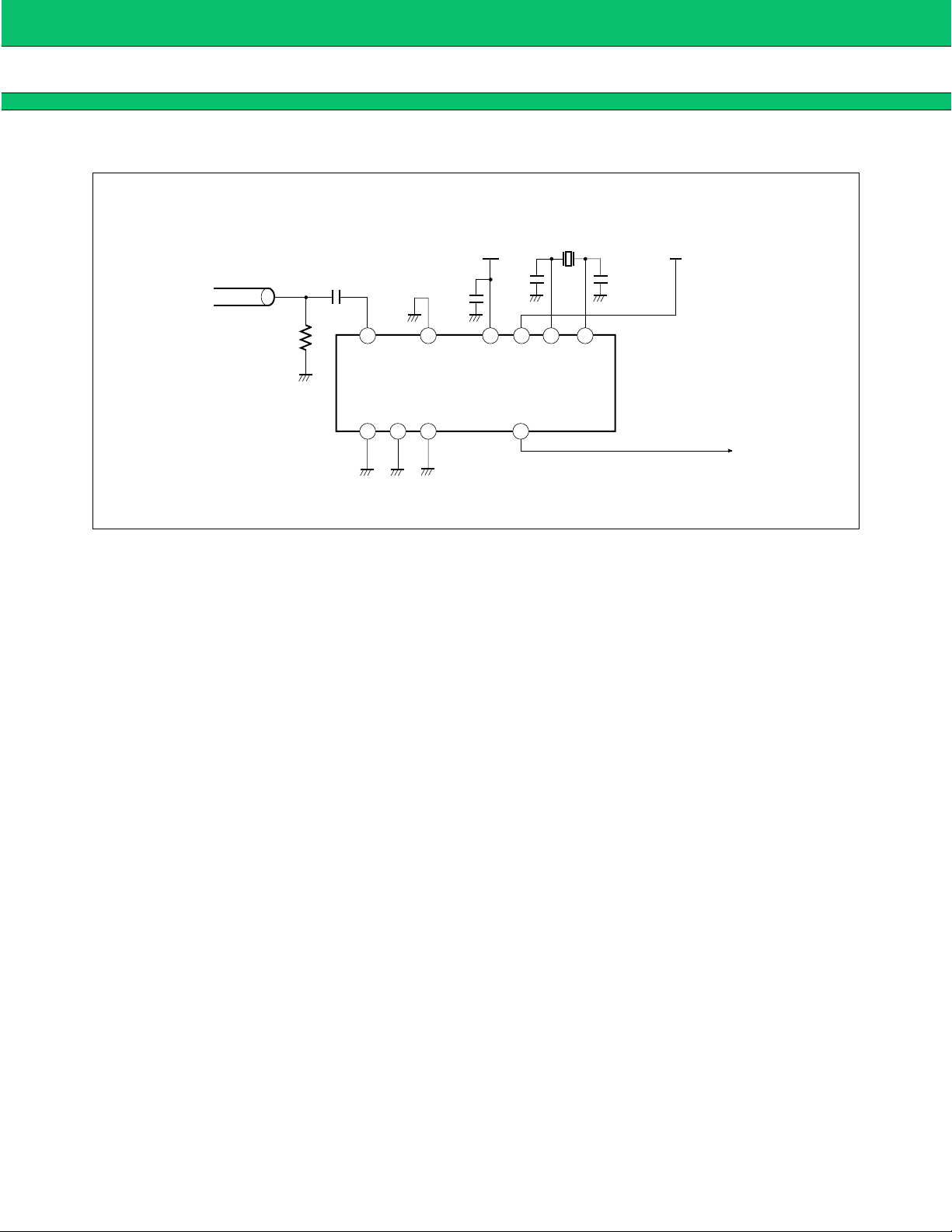
MEASURMENT CIRCUIT
P • G
50 Ω
CC
= 3 V
V
1000 pF
0.1 µF
10 7 5 4 3 1
141311
17
X'tal
VP = 6 V
Oscilloscope
12
Page 13
■
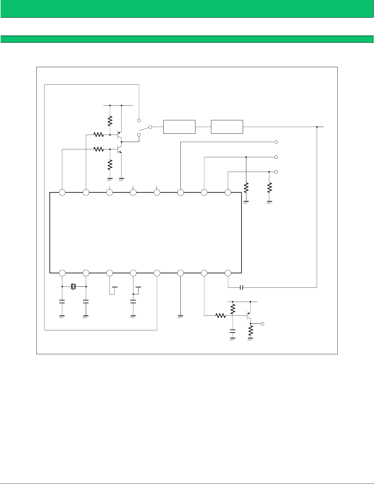
TYPICAL APPLICATION EXAMPLE
VPX (6V)
MB1511
10 kΩ
15
L P F V C O
14
LE
13
Data
100 kΩ
12 kΩ
12 kΩ
10 kΩ
20
φR
OSC
1 3 4 5 6 7 8 10
18
φP
IN OSC OUT V P V CC D O GND LD fin
X'tal
C
1 C 2
17
fout
6 V 3 V
0.1 µF
16
BiSW
FC
MB1511
11
Clock
1000 pF
V
CC (3 V)
OUTPUT
From Controller
47 kΩ 47 kΩ
VPX, VP:8V max.
1
C
, C2: Depends on crystal oscillator
LE, FC : With internal pull up resistor
φP : Open drain output
33 kΩ
0.01 µF
Lock Detector
10 kΩ
13
Page 14
MB1511
■
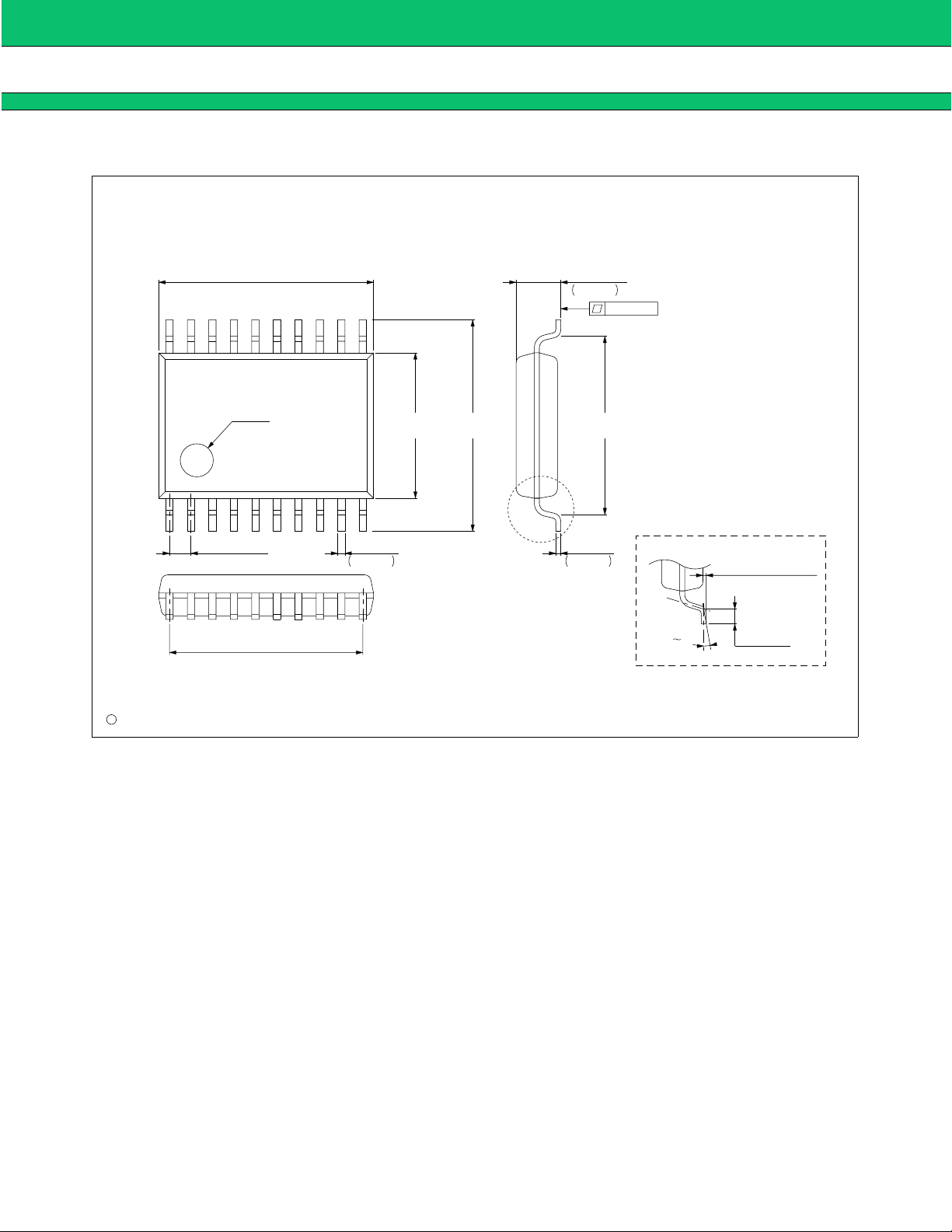
PACKAGE DIMENSION
20 pin, Plastic SSOP
(FPT-20P-M03)
*: This dimension does not include resin protruction.
*
6.50±0.10(.256±.004)
INDEX
0.65±0.12
(.0256±.0047)
5.85(.230)REF
C
1994 FUJITSU LIMITED F20012S-2C-4
0.22
.009
1.25
.049
*
4.40±0.10 5.40(.213)
(.173±.004) (.252±.008) NOM
+0.10
–0.05
+.004
–.002
6.40±0.20
"A"
0.15
.006
+0.20
–0.10
+.008
–.004
0.10(.004)
+0.05
–0.02
+.002
–.001
Details of "A" part
0 10°
Dimensions in mm (inches).
0.10±0.10(.004±.004)
(STAND OFF)
0.50±0.20
(.020±.008)
14
Page 15

MB1511
FUJITSU LIMITED
For further information please contact:
Japan
FUJITSU LIMITED
Corporate Global Business Support Division
Electronic Devices
KAWASAKI PLANT, 4-1-1, Kamikodanaka
Nakahara-ku, Kaw asaki-shi
Kanagawa 211-8588, Japan
Tel: (044) 754-3763
Fax: (044) 754-3329
All Rights Reserved.
The contents of this document are subject to change without
notice. Customers are advised t o consult with FUJITSU sales
representatives before ordering.
http://www.fujitsu.co.jp/
North and South America
FUJITSU MICROELECTRONICS, INC.
Semiconductor Division
3545 North First Street
San Jose, CA 95134-1804, USA
Tel: (408) 922-9000
Fax: (408) 922-9179
Customer Response Center
Mon. - Fri.: 7 am - 5 pm (PST)
Tel: (800) 866-8608
Fax: (408) 922-9179
http://www.fujitsumicro.com/
Europe
FUJITSU MIKROELEKTRONIK GmbH
Am Siebenstein 6-10
D-63303 Dreieich-Buchschlag
Germany
Tel: (06103) 690-0
Fax: (06103) 690-122
http://www.fujitsu-ede.com/
Asia Pacific
FUJITSU MICROELECTRO NICS ASIA PTE LTD
#05-08, 151 Lorong Chuan
New Tech Park
Singapore 556741
Tel: (65) 281-0770
Fax: (65) 281-0220
http://www.fmap.com.sg/
The information and circuit diagrams in this document presented
as examples of semicondu c t or device applications, and ar e not
intended to be incorporated in devices for actual use. Also,
FUJITSU is unable to assume responsibility for infringement of
any patent rights or other righ ts of third pa rtie s arisin g fro m t he
use of this information or circuit diagrams.
FUJITSU semiconductor devices are intended for use in
standard applications (computers, office automation and other
office equipment, industrial, communications, and measurement
equipment, personal or household devices, etc.).
CAUTION:
Customers consideri ng the use of our products in special
applications where failure or abnormal operation may directly
affect human lives or cause physical injury or property damage,
or where extremely high levels of reli ability are demanded (such
as aerospace systems, atomic energy controls, sea floor
repeaters, vehicle operatin g controls, medical devices for life
support, etc.) are requested to consult with FUJITSU sales
representatives before such use. The company will not be
responsible for damages arising from such use without prior
approval.
Any semiconductor devices have inherently a certain rate of
failure. You must protect against injury, damage or loss from
such failures by incorporating sa fet y desi gn meas ures in to y our
facility and equipment su ch as redundancy, fire protection, and
prevention of over-current levels and other abnormal operating
conditions.
If any products descri be d in th is doc um e nt re pr e sen t goods or
technologies subject to certain restrictions on export under the
Foreign Exchange and Foreign Trade Control Law of Japan, the
prior authorization by Japanese government should be required
for export of those products from Japan.
16
F9803
FUJITSU LIMITED Printed in Japan
 Loading...