

Page 1

Click here to ask about the production status of specific part numbers.
MAX78000 Ultra-Low-Power Arm Cortex-M4 Processor
with FPU-Based Microcontroller with
Convolutional Neural Network Accelerator
General Description
Artificial intelligence (AI) requires extreme computational
horsepower, but Maxim is cutting the power cord from
AI insights. The MAX78000 is a new breed of AI microcontroller built to enable neural networks to execute
at ultra-low power and live at the edge of the IoT. This
product combines the most energy-efficient AI processing
with Maxim's proven ultra-low power microcontrollers. Our
hardware-based convolutional neural network (CNN) accelerator enables battery-powered applications to execute
AI inferences while spending only microjoules of energy.
The MAX78000 is an advanced system-on-chip featuring
an Arm®Cortex®-M4 with FPU CPU for efficient system
control with an ultra-low-power deep neural network accelerator. The CNN engine has a weight storage memory of
442KB, and can support 1-, 2-, 4-, and 8-bit weights (supporting networks of up to 3.5 million weights). The CNN
weight memory is SRAM-based, so AI network updates
can be made on the fly. The CNN engine also has 512KB
of data memory. The CNN architecture is highly flexible,
allowing networks to be trained in conventional toolsets
like PyTorch and TensorFlow®, then converted for execution on the MAX78000 using tools provided by Maxim.
In addition to the memory in the CNN engine, the
MAX78000 has large on-chip system memory for the microcontroller core, with 512KB flash and up to 128KB
SRAM. Multiple high-speed and low-power communications interfaces are supported, including I2S and a parallel
camera interface (PCIF).
The device is available in 81-pin CTBGA (8mm x 8mm,
0.8mm pitch) and 130-pin WLP (4.6mm x 3.7mm, 0.35mm
pitch) packages.
Applications
● Object Detection and Classification
● Audio Processing: Multi-Keyword Recognition, Sound
Classification, Noise Cancellation
● Facial Recognition
● Time-Series Data Processing: Heart Rate/Health
Signal Analysis, Multi-Sensor Analysis, Predictive
Maintenance
Benefits and Features
● Dual Core Ultra-Low-Power Microcontroller
• Arm Cortex-M4 Processor with FPU Up to 100MHz
• 512KB Flash and 128KB SRAM
• Optimized Performance with 16KB Instruction
Cache
• Optional Error Correction Code (ECC-SEC-DED)
for SRAM
• 32-Bit RISC-V Coprocessor up to 60MHz
• Up to 52 General-Purpose I/O Pins
• 12-Bit Parallel Camera Interface
• One I2S Master/Slave for Digital Audio Interface
● Neural Network Accelerator
• Highly Optimaized for Deep Convolutional Neural
Networks
• 442k 8bit Weight Capacity with 1,2,4,8-bit Weights
• Programmable Input Image Size up to 1024 x 1024
pixels
• Programmable Network Depth up to 64 Layers
• Programmable per Layer Network Channel Widths
up to 1024 Channels
• 1 and 2 Dimensional Convolution Processing
• Streaming Mode
• Flexibility to Support Other Network Types,
Including MLP and Recurrent Neural Networks
● Power Management Maximizes Operating Time for
Battery Applications
• Integrated Single-Inductor Multiple-Output (SIMO)
Switch-Mode Power Supply (SMPS)
• 2.0V to 3.6V SIMO Supply Voltage Range
• Dynamic Voltage Scaling Minimizes Active Core
Power Consumption
• 22.2μA/MHz While Loop Execution at 3.0V from
Cache (CM4 only)
• Selectable SRAM Retention in Low-Power Modes
with Real-Time Clock (RTC) Enabled
● Security and Integrity
• Available Secure Boot
• AES 128/192/256 Hardware Acceleration Engine
• True Random Number Generator (TRNG) Seed
Generator
Ordering Information appears at end of data sheet.
Arm and Cortex are registered trademarks of Arm Limited (or its subsidiaries) in the US and/or elsewhere.
PyTorch is a trademark of Facebook, Inc.
TensorFlow is a trademark of Google, Inc.
19-100868; Rev 0; 8/20
Page 2
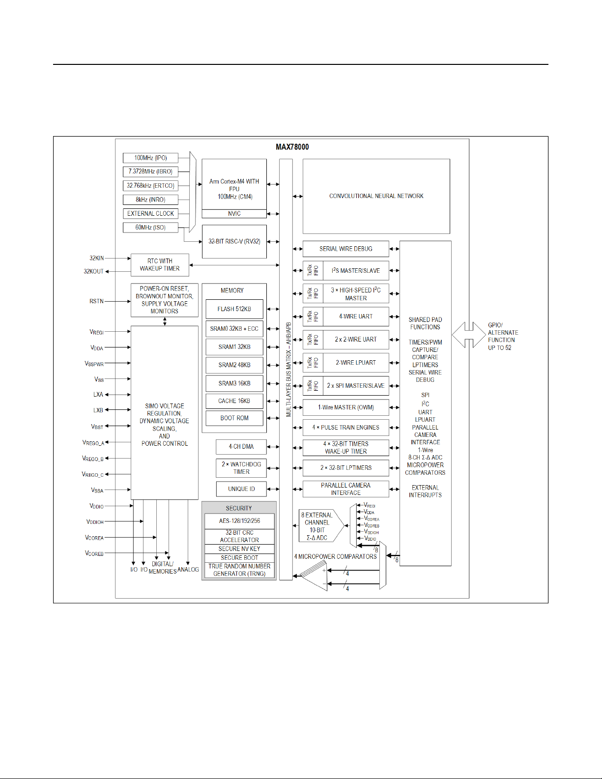
MAX78000 Ultra-Low-Power Arm Cortex-M4 Processor with
FPU-Based Microcontroller with Convolutional
Neural Network Accelerator
Simplified Block Diagram
www.maximintegrated.com
19-100868
Maxim Integrated | 2
Page 3

MAX78000 Ultra-Low-Power Arm Cortex-M4 Processor with
FPU-Based Microcontroller with Convolutional
Neural Network Accelerator
TABLE OF CONTENTS
General Description. . . . . . . . . . . . . . . . . . . . . . . . . . . . . . . . . . . . . . . . . . . . . . . . . . . . . . . . . . . . . . . . . . . . . . . . . . . . . . 1
Applications . . . . . . . . . . . . . . . . . . . . . . . . . . . . . . . . . . . . . . . . . . . . . . . . . . . . . . . . . . . . . . . . . . . . . . . . . . . . . . . . . . . . 1
Benefits and Features . . . . . . . . . . . . . . . . . . . . . . . . . . . . . . . . . . . . . . . . . . . . . . . . . . . . . . . . . . . . . . . . . . . . . . . . . . . . 1
Simplified Block Diagram . . . . . . . . . . . . . . . . . . . . . . . . . . . . . . . . . . . . . . . . . . . . . . . . . . . . . . . . . . . . . . . . . . . . . . . . . 2
Absolute Maximum Ratings. . . . . . . . . . . . . . . . . . . . . . . . . . . . . . . . . . . . . . . . . . . . . . . . . . . . . . . . . . . . . . . . . . . . . . . . 7
Package Information . . . . . . . . . . . . . . . . . . . . . . . . . . . . . . . . . . . . . . . . . . . . . . . . . . . . . . . . . . . . . . . . . . . . . . . . . . . . . 7
81-CTBGA . . . . . . . . . . . . . . . . . . . . . . . . . . . . . . . . . . . . . . . . . . . . . . . . . . . . . . . . . . . . . . . . . . . . . . . . . . . . . . . . . . 7
Electrical Characteristics . . . . . . . . . . . . . . . . . . . . . . . . . . . . . . . . . . . . . . . . . . . . . . . . . . . . . . . . . . . . . . . . . . . . . . . . . 7
Electrical Characteristics—SPI . . . . . . . . . . . . . . . . . . . . . . . . . . . . . . . . . . . . . . . . . . . . . . . . . . . . . . . . . . . . . . . . . . . . 18
Electrical Characteristics—I2C . . . . . . . . . . . . . . . . . . . . . . . . . . . . . . . . . . . . . . . . . . . . . . . . . . . . . . . . . . . . . . . . . . . . 19
Electrical Characteristics—I2S . . . . . . . . . . . . . . . . . . . . . . . . . . . . . . . . . . . . . . . . . . . . . . . . . . . . . . . . . . . . . . . . . . . . 21
Electrical Characteristics—PCIF . . . . . . . . . . . . . . . . . . . . . . . . . . . . . . . . . . . . . . . . . . . . . . . . . . . . . . . . . . . . . . . . . . 22
Electrical Characteristics—1-Wire Master . . . . . . . . . . . . . . . . . . . . . . . . . . . . . . . . . . . . . . . . . . . . . . . . . . . . . . . . . . . 22
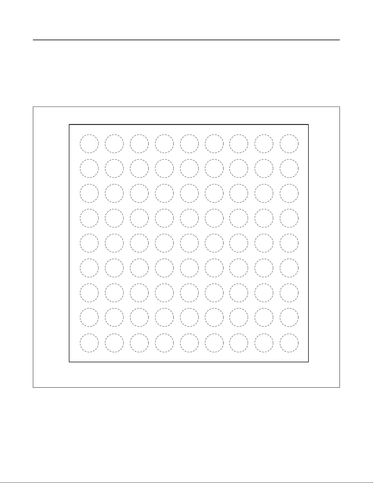
Pin Configuration. . . . . . . . . . . . . . . . . . . . . . . . . . . . . . . . . . . . . . . . . . . . . . . . . . . . . . . . . . . . . . . . . . . . . . . . . . . . . . . 27
81 CTBGA . . . . . . . . . . . . . . . . . . . . . . . . . . . . . . . . . . . . . . . . . . . . . . . . . . . . . . . . . . . . . . . . . . . . . . . . . . . . . . . . . 27
Pin Description . . . . . . . . . . . . . . . . . . . . . . . . . . . . . . . . . . . . . . . . . . . . . . . . . . . . . . . . . . . . . . . . . . . . . . . . . . . . . . . . 28
Detailed Description . . . . . . . . . . . . . . . . . . . . . . . . . . . . . . . . . . . . . . . . . . . . . . . . . . . . . . . . . . . . . . . . . . . . . . . . . . . . 32
Arm Cortex-M4 with FPU Processor and RISC-V RV32 Processor . . . . . . . . . . . . . . . . . . . . . . . . . . . . . . . . . . . . . . 32
Convolutional Neural Network Accelerator (CNN) . . . . . . . . . . . . . . . . . . . . . . . . . . . . . . . . . . . . . . . . . . . . . . . . . . . 32
Memory . . . . . . . . . . . . . . . . . . . . . . . . . . . . . . . . . . . . . . . . . . . . . . . . . . . . . . . . . . . . . . . . . . . . . . . . . . . . . . . . . . . 34
Internal Flash Memory. . . . . . . . . . . . . . . . . . . . . . . . . . . . . . . . . . . . . . . . . . . . . . . . . . . . . . . . . . . . . . . . . . . . . . 34
Internal SRAM . . . . . . . . . . . . . . . . . . . . . . . . . . . . . . . . . . . . . . . . . . . . . . . . . . . . . . . . . . . . . . . . . . . . . . . . . . . . 34
Comparators. . . . . . . . . . . . . . . . . . . . . . . . . . . . . . . . . . . . . . . . . . . . . . . . . . . . . . . . . . . . . . . . . . . . . . . . . . . . . . . . 34
Dynamic Voltage Scaling (DVS) Controller . . . . . . . . . . . . . . . . . . . . . . . . . . . . . . . . . . . . . . . . . . . . . . . . . . . . . . . . 34
Clocking Scheme . . . . . . . . . . . . . . . . . . . . . . . . . . . . . . . . . . . . . . . . . . . . . . . . . . . . . . . . . . . . . . . . . . . . . . . . . . . . 34
General-Purpose I/O and Special Function Pins . . . . . . . . . . . . . . . . . . . . . . . . . . . . . . . . . . . . . . . . . . . . . . . . . . . . 35
Parallel Camera Interface (PCIF) . . . . . . . . . . . . . . . . . . . . . . . . . . . . . . . . . . . . . . . . . . . . . . . . . . . . . . . . . . . . . . . . 36
Analog-to-Digital Converter . . . . . . . . . . . . . . . . . . . . . . . . . . . . . . . . . . . . . . . . . . . . . . . . . . . . . . . . . . . . . . . . . . . . 36
Single-Inductor Multiple-Output Switch-Mode Power Supply (SIMO SMPS) . . . . . . . . . . . . . . . . . . . . . . . . . . . . . . . 36
Power Management . . . . . . . . . . . . . . . . . . . . . . . . . . . . . . . . . . . . . . . . . . . . . . . . . . . . . . . . . . . . . . . . . . . . . . . . . . 37
Power Management Unit. . . . . . . . . . . . . . . . . . . . . . . . . . . . . . . . . . . . . . . . . . . . . . . . . . . . . . . . . . . . . . . . . . . . 37
ACTIVE Mode . . . . . . . . . . . . . . . . . . . . . . . . . . . . . . . . . . . . . . . . . . . . . . . . . . . . . . . . . . . . . . . . . . . . . . . . . . . . 37
SLEEP Mode. . . . . . . . . . . . . . . . . . . . . . . . . . . . . . . . . . . . . . . . . . . . . . . . . . . . . . . . . . . . . . . . . . . . . . . . . . . . . 37
LOW POWER Mode (LPM). . . . . . . . . . . . . . . . . . . . . . . . . . . . . . . . . . . . . . . . . . . . . . . . . . . . . . . . . . . . . . . . . . 37
MICRO POWER Mode (μPM) . . . . . . . . . . . . . . . . . . . . . . . . . . . . . . . . . . . . . . . . . . . . . . . . . . . . . . . . . . . . . . . . 37
STANDBY Mode . . . . . . . . . . . . . . . . . . . . . . . . . . . . . . . . . . . . . . . . . . . . . . . . . . . . . . . . . . . . . . . . . . . . . . . . . . 38
BACKUP Mode . . . . . . . . . . . . . . . . . . . . . . . . . . . . . . . . . . . . . . . . . . . . . . . . . . . . . . . . . . . . . . . . . . . . . . . . . . . 38
POWER DOWN Mode (PDM) . . . . . . . . . . . . . . . . . . . . . . . . . . . . . . . . . . . . . . . . . . . . . . . . . . . . . . . . . . . . . . . . 39
www.maximintegrated.com
19-100868
Maxim Integrated | 3
Page 4

MAX78000 Ultra-Low-Power Arm Cortex-M4 Processor with
FPU-Based Microcontroller with Convolutional
Neural Network Accelerator
TABLE OF CONTENTS (CONTINUED)
Wakeup Sources . . . . . . . . . . . . . . . . . . . . . . . . . . . . . . . . . . . . . . . . . . . . . . . . . . . . . . . . . . . . . . . . . . . . . . . . . . 39
Real-Time Clock. . . . . . . . . . . . . . . . . . . . . . . . . . . . . . . . . . . . . . . . . . . . . . . . . . . . . . . . . . . . . . . . . . . . . . . . . . . . . 39
Programmable Timers . . . . . . . . . . . . . . . . . . . . . . . . . . . . . . . . . . . . . . . . . . . . . . . . . . . . . . . . . . . . . . . . . . . . . . . . 39
32-Bit Timer/Counter/PWM (TMR, LPTMR) . . . . . . . . . . . . . . . . . . . . . . . . . . . . . . . . . . . . . . . . . . . . . . . . . . . . . 40
Watchdog Timer (WDT) . . . . . . . . . . . . . . . . . . . . . . . . . . . . . . . . . . . . . . . . . . . . . . . . . . . . . . . . . . . . . . . . . . . . 41
Pulse Train Engine (PT) . . . . . . . . . . . . . . . . . . . . . . . . . . . . . . . . . . . . . . . . . . . . . . . . . . . . . . . . . . . . . . . . . . . . 41
Serial Peripherals . . . . . . . . . . . . . . . . . . . . . . . . . . . . . . . . . . . . . . . . . . . . . . . . . . . . . . . . . . . . . . . . . . . . . . . . . . . . 41
I2C Interface (I2C) . . . . . . . . . . . . . . . . . . . . . . . . . . . . . . . . . . . . . . . . . . . . . . . . . . . . . . . . . . . . . . . . . . . . . . . . . 41
I2S Interface (I2S) . . . . . . . . . . . . . . . . . . . . . . . . . . . . . . . . . . . . . . . . . . . . . . . . . . . . . . . . . . . . . . . . . . . . . . . . . 42
Serial Peripheral Interface (SPI) . . . . . . . . . . . . . . . . . . . . . . . . . . . . . . . . . . . . . . . . . . . . . . . . . . . . . . . . . . . . . . 42
UART (UART, LPUART) . . . . . . . . . . . . . . . . . . . . . . . . . . . . . . . . . . . . . . . . . . . . . . . . . . . . . . . . . . . . . . . . . . . . 43
1-Wire Master (OWM) . . . . . . . . . . . . . . . . . . . . . . . . . . . . . . . . . . . . . . . . . . . . . . . . . . . . . . . . . . . . . . . . . . . . . . 44
Standard DMA Controller . . . . . . . . . . . . . . . . . . . . . . . . . . . . . . . . . . . . . . . . . . . . . . . . . . . . . . . . . . . . . . . . . . . . . . 44
Security . . . . . . . . . . . . . . . . . . . . . . . . . . . . . . . . . . . . . . . . . . . . . . . . . . . . . . . . . . . . . . . . . . . . . . . . . . . . . . . . . . . 44
AES . . . . . . . . . . . . . . . . . . . . . . . . . . . . . . . . . . . . . . . . . . . . . . . . . . . . . . . . . . . . . . . . . . . . . . . . . . . . . . . . . . . . 44
True Random Number Generator (TRNG) Non-Deterministic Random Bit Generator (NDRBG). . . . . . . . . . . . . 44
CRC Module . . . . . . . . . . . . . . . . . . . . . . . . . . . . . . . . . . . . . . . . . . . . . . . . . . . . . . . . . . . . . . . . . . . . . . . . . . . . . 44
Bootloader . . . . . . . . . . . . . . . . . . . . . . . . . . . . . . . . . . . . . . . . . . . . . . . . . . . . . . . . . . . . . . . . . . . . . . . . . . . . . . . 45
Secure Bootloader. . . . . . . . . . . . . . . . . . . . . . . . . . . . . . . . . . . . . . . . . . . . . . . . . . . . . . . . . . . . . . . . . . . . . . . . . 45
Debug and Development Interface (SWD, JTAG) . . . . . . . . . . . . . . . . . . . . . . . . . . . . . . . . . . . . . . . . . . . . . . . . . . . 45
Applications Information . . . . . . . . . . . . . . . . . . . . . . . . . . . . . . . . . . . . . . . . . . . . . . . . . . . . . . . . . . . . . . . . . . . . . . . . . 46
Bypass Capacitors . . . . . . . . . . . . . . . . . . . . . . . . . . . . . . . . . . . . . . . . . . . . . . . . . . . . . . . . . . . . . . . . . . . . . . . . . . . 46
Ordering Information . . . . . . . . . . . . . . . . . . . . . . . . . . . . . . . . . . . . . . . . . . . . . . . . . . . . . . . . . . . . . . . . . . . . . . . . . . . . 46
Revision History . . . . . . . . . . . . . . . . . . . . . . . . . . . . . . . . . . . . . . . . . . . . . . . . . . . . . . . . . . . . . . . . . . . . . . . . . . . . . . . 47
www.maximintegrated.com
19-100868
Maxim Integrated | 4
Page 5

MAX78000 Ultra-Low-Power Arm Cortex-M4 Processor with
FPU-Based Microcontroller with Convolutional
Neural Network Accelerator
LIST OF FIGURES
Figure 1. SPI Master Mode Timing Diagram . . . . . . . . . . . . . . . . . . . . . . . . . . . . . . . . . . . . . . . . . . . . . . . . . . . . . . . . . . 23
Figure 2. SPI Slave Mode Timing Diagram . . . . . . . . . . . . . . . . . . . . . . . . . . . . . . . . . . . . . . . . . . . . . . . . . . . . . . . . . . . 23
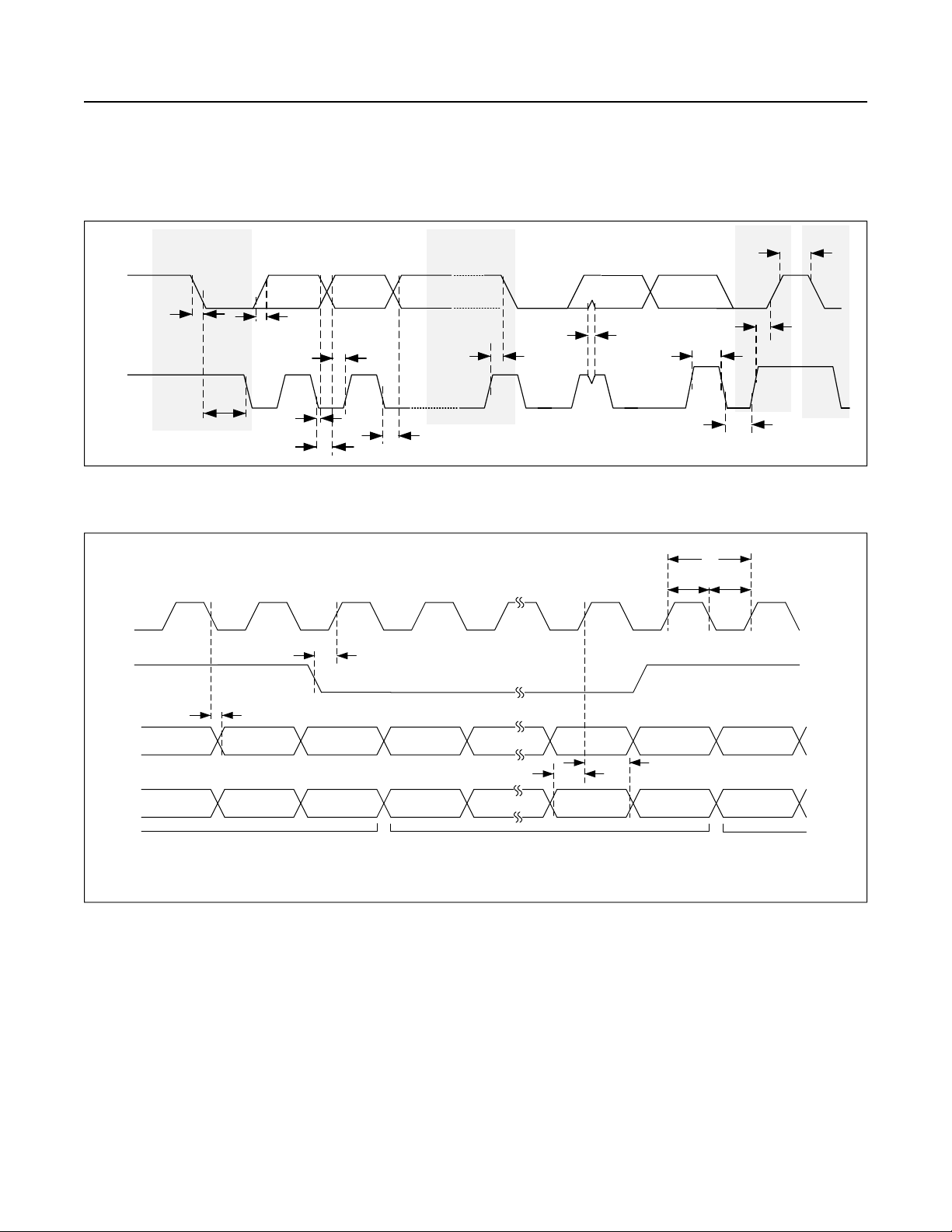
Figure 3. I2C Timing Diagram . . . . . . . . . . . . . . . . . . . . . . . . . . . . . . . . . . . . . . . . . . . . . . . . . . . . . . . . . . . . . . . . . . . . . 24
Figure 4. I2S Timing Diagram . . . . . . . . . . . . . . . . . . . . . . . . . . . . . . . . . . . . . . . . . . . . . . . . . . . . . . . . . . . . . . . . . . . . . 24
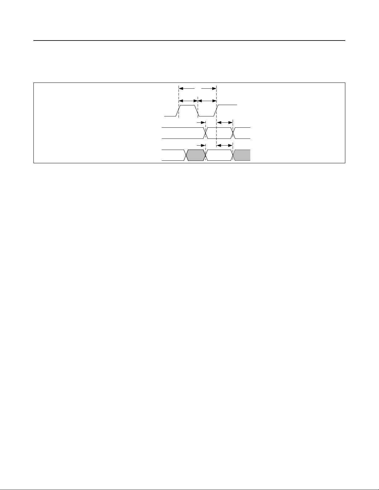
Figure 5. Parallel Camera Interface Timing Diagram . . . . . . . . . . . . . . . . . . . . . . . . . . . . . . . . . . . . . . . . . . . . . . . . . . . 25
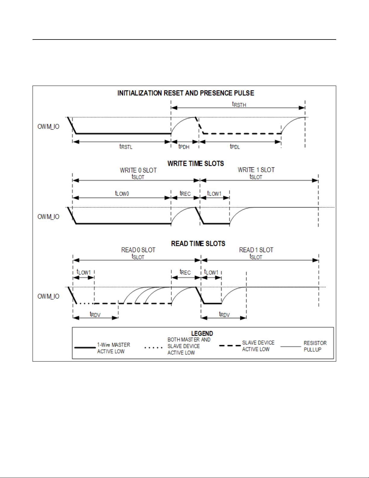
Figure 6. 1-Wire Master Data Timing Diagram . . . . . . . . . . . . . . . . . . . . . . . . . . . . . . . . . . . . . . . . . . . . . . . . . . . . . . . . 26
Figure 7. Clocking Scheme Diagram. . . . . . . . . . . . . . . . . . . . . . . . . . . . . . . . . . . . . . . . . . . . . . . . . . . . . . . . . . . . . . . . 35
www.maximintegrated.com
19-100868
Maxim Integrated | 5
Page 6

MAX78000 Ultra-Low-Power Arm Cortex-M4 Processor with
FPU-Based Microcontroller with Convolutional
Neural Network Accelerator
LIST OF TABLES
Table 1. BACKUP Mode SRAM Retention . . . . . . . . . . . . . . . . . . . . . . . . . . . . . . . . . . . . . . . . . . . . . . . . . . . . . . . . . . . 39
Table 2. Wakeup Sources . . . . . . . . . . . . . . . . . . . . . . . . . . . . . . . . . . . . . . . . . . . . . . . . . . . . . . . . . . . . . . . . . . . . . . . . 39
Table 3. Timer Configuration Options . . . . . . . . . . . . . . . . . . . . . . . . . . . . . . . . . . . . . . . . . . . . . . . . . . . . . . . . . . . . . . . 40
Table 4. Watchdog Timer Configuration Options . . . . . . . . . . . . . . . . . . . . . . . . . . . . . . . . . . . . . . . . . . . . . . . . . . . . . . 41
Table 5. SPI Configuration Options . . . . . . . . . . . . . . . . . . . . . . . . . . . . . . . . . . . . . . . . . . . . . . . . . . . . . . . . . . . . . . . . . 43
Table 6. UART Configuration Options . . . . . . . . . . . . . . . . . . . . . . . . . . . . . . . . . . . . . . . . . . . . . . . . . . . . . . . . . . . . . . . 43
Table 7. Common CRC Polynomials. . . . . . . . . . . . . . . . . . . . . . . . . . . . . . . . . . . . . . . . . . . . . . . . . . . . . . . . . . . . . . . . 45
www.maximintegrated.com
19-100868
Maxim Integrated | 6
Page 7
MAX78000 Ultra-Low-Power Arm Cortex-M4 Processor with
FPU-Based Microcontroller with Convolutional
Neural Network Accelerator
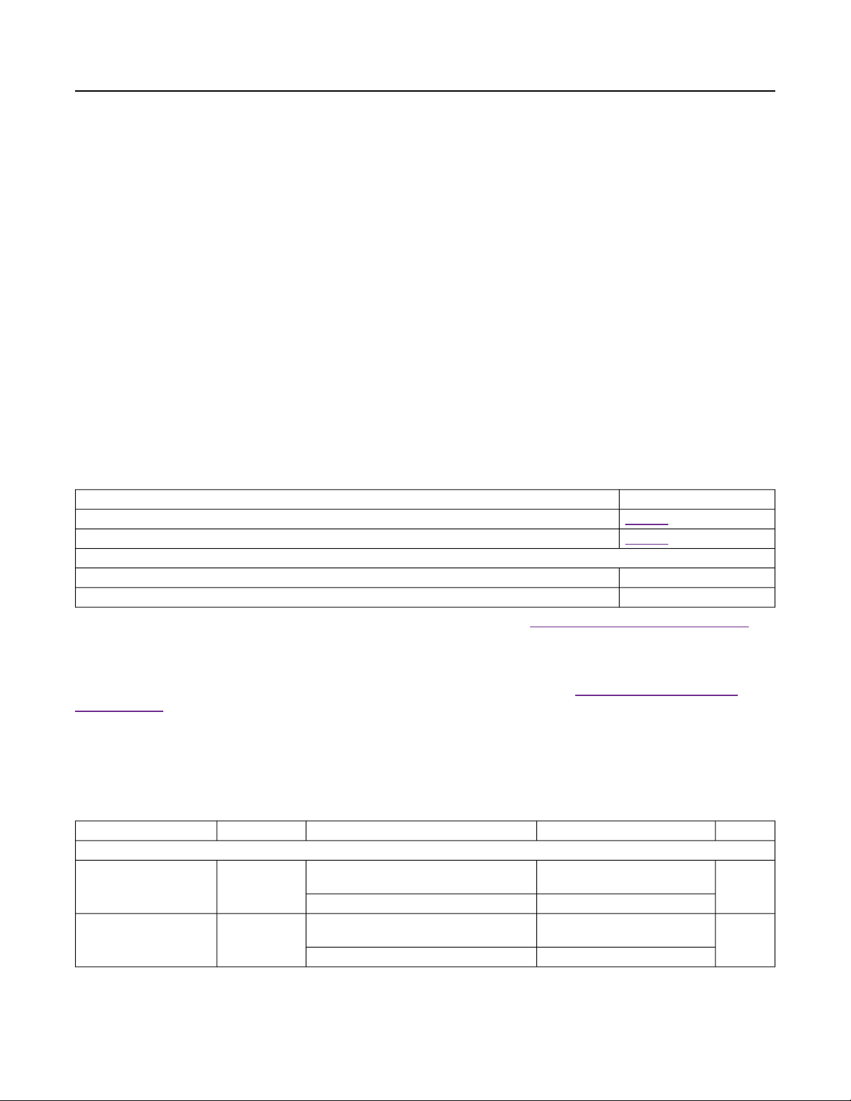
Absolute Maximum Ratings
V
V
V
V
V
GPIO (V
RSTN, GPIO (V
32KIN, 32KOUT ......................................... -0.3V to V
V
V
V
Stresses beyond those listed under “Absolute Maximum Ratings” may cause permanent damage to the device. These are stress ratings only, and functional operation of the
device at these or any other conditions beyond those indicated in the operational sections of the specifications is not implied. Exposure to absolute maximum rating conditions for
extended periods may affect device reliability.
Package Information
81-CTBGA
, V
COREA
.................................................................... -0.3V to +3.6V
DDIO
.................................................................. -0.3V to +3.6V
DDIOH
.................................................................... -0.3V to +3.6V
REGI
................................................................... -0.3V to +1.89V
DDA
DDIO
Combined Pins (sink) ............................................. 100mA
DDIO
Combined Pins (sink)........................................... 100mA
DDIOH
.................................................................................. 100mA
SSA
Package Code X8188+3C
Outline Number 21-0735
Land Pattern Number 90-0460
Thermal Resistance, Four-Layer Board:
Junction-to-Ambient (θJA) 33.55ºC/W
Junction-to-Case Thermal Resistance (θJC) 6.73ºC/W
............................................... -0.3V to +1.21V
COREB
)............................................ -0.3V to V
)............................-0.3V to V
DDIOH
DDIO
DDIOH
DDA
+ 0.5V
+ 0.5V
+ 0.2V
VSS....................................................................................200mA
V
Output Current (sink) by any GPIO Pin................................25mA
Output Current (source) by any GPIO Pin ......................... -25mA
Continuous Package Power Dissipation CTBGA (multilayer
board) TA= +70°C (derate 29.81mW/°C above
+70°C)........................................................................2384.50mW
Operating Temperature Range ...........................-40°C to +105°C
Storage Temperature Range ..............................-65°C to +150°C
Soldering Temperature .....................................................+260°C
.............................................................................100mA
SSPWR
For the latest package outline information and land patterns (footprints), go to www.maximintegrated.com/packages.
Note that a “+”, “#”, or “-” in the package code indicates RoHS status only. Package drawings may show a different
suffix character, but the drawing pertains to the package regardless of RoHS status.
Package thermal resistances were obtained using the method described in JEDEC specification JESD51-7, using a
four-layer board. For detailed information on package thermal considerations, refer to www.maximintegrated.com/
thermal-tutorial.
Electrical Characteristics
(Limits are 100% tested at TA= +25°C and TA= +105°C. TYP specifications are provided for TA= +25°C. Limits over the operating
temperature range and relevant supply voltage range are guaranteed by design and characterization. Specifications marked GBD are
guaranteed by design and not production tested. Specifications to the minimum operating temperature are guaranteed by design and
are not production tested. GPIO are only tested at TA= +105°C.)
PARAMETER SYMBOL CONDITIONS MIN TYP MAX UNITS
POWER SUPPLIES
V
Core Input Supply
Voltage A
Core Input Supply
Voltage B
V
COREA
V
COREB
Falling
Rising 0.9 1.1 1.21
Falling
Rising 0.9 1.1 1.21
COREA
V
RST
V
COREB
V
RST
1.1 1.21
1.1 1.21
V
V
www.maximintegrated.com
19-100868
Maxim Integrated | 7
Page 8
MAX78000 Ultra-Low-Power Arm Cortex-M4 Processor with
FPU-Based Microcontroller with Convolutional
Neural Network Accelerator
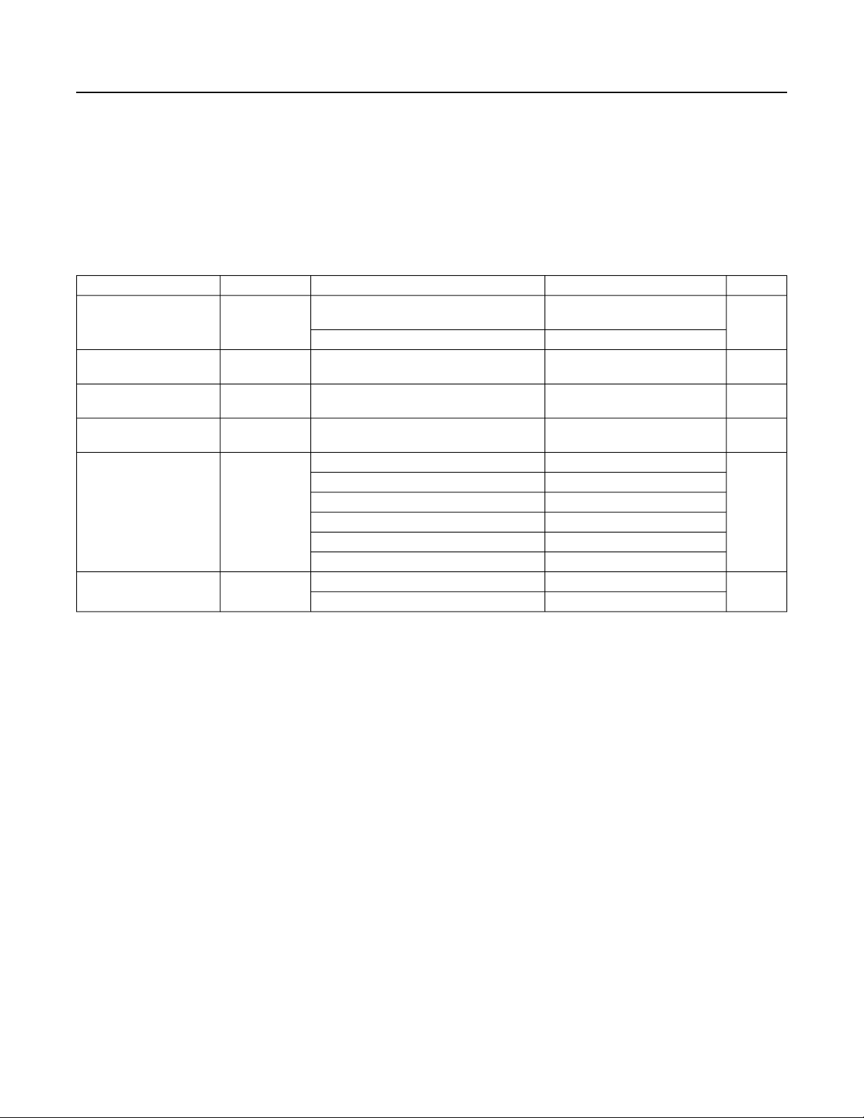
Electrical Characteristics (continued)
(Limits are 100% tested at TA= +25°C and TA= +105°C. TYP specifications are provided for TA= +25°C. Limits over the operating
temperature range and relevant supply voltage range are guaranteed by design and characterization. Specifications marked GBD are
guaranteed by design and not production tested. Specifications to the minimum operating temperature are guaranteed by design and
are not production tested. GPIO are only tested at TA= +105°C.)
PARAMETER SYMBOL CONDITIONS MIN TYP MAX UNITS
V
Input Supply Voltage,
Battery
Input Supply Voltage,
Analog
Input Supply Voltage,
GPIO
Input Supply Voltage,
GPIO (High)
Power-Fail Reset
Voltage
Power-On Reset
Voltage
V
REGI
V
DDA
V
DDIO
V
DDIOH
V
RST
V
POR
Falling
Rising 2.45 3.0 3.6
Monitors V
Monitors V
Monitors V
Monitors V
Monitors V
Monitors V
Monitors V
Monitors V
COREA
COREB
DDA
DDIO
DDIOH
REGI
COREA
DDA
REGI
V
RST
1.71 1.8 1.89 V
1.71 1.8 1.89 V
1.71 3.0 3.6 V
0.72 0.77
1.58 1.64 1.69
1.58 1.64 1.69
1.58 1.64 1.69
1.91 1.98 2.08
3.0 3.6
0.76
0.63
1.25
V
V
V
www.maximintegrated.com
19-100868
Maxim Integrated | 8
Page 9

MAX78000 Ultra-Low-Power Arm Cortex-M4 Processor with
FPU-Based Microcontroller with Convolutional
Neural Network Accelerator
Electrical Characteristics (continued)
(Limits are 100% tested at TA= +25°C and TA= +105°C. TYP specifications are provided for TA= +25°C. Limits over the operating
temperature range and relevant supply voltage range are guaranteed by design and characterization. Specifications marked GBD are
guaranteed by design and not production tested. Specifications to the minimum operating temperature are guaranteed by design and
are not production tested. GPIO are only tested at TA= +105°C.)
PARAMETER SYMBOL CONDITIONS MIN TYP MAX UNITS
V
Current, ACTIVE
REGI
Mode
I
REGI_DACT
I
REGI_FACT
Dynamic, IPO enabled, f
100MHz, total current into V
V
= 3.0V, V
REGI
COREA
SYS_CLK(MAX)
REGI
= V
COREB
1.1V, CM4 in Active mode executing
CoreMark®, RV32 in ACTIVE mode
executing While(1), ECC disabled, all
CNN quadrants disabled, all CNN
memory disabled; inputs tied to VSS,
V
DDIO
, or V
; outputs source/sink
DDIOH
0mA
Dynamic, IPO enabled, f
100MHz, total current into V
V
= 3.0V, V
REGI
COREA
SYS_CLK(MAX)
REGI
= V
COREB
1.1V, CM4 and RV32 in ACTIVE mode
executing While(1), ECC disabled, all
CNN quadrants disabled, all CNN
memory disabled; inputs tied to VSS,
V
DDIO
, or V
; outputs source/sink
DDIOH
0mA
Dynamic, IPO enabled, f
100MHz, total current into V
V
= 3.0V, V
REGI
COREA
SYS_CLK(MAX)
REGI
= V
COREB
1.1V, CM4 in ACTIVE mode executing
While(1), RV32 in SLEEP mode, ECC
disabled, all CNN quadrants disabled, all
CNN memory disabled; inputs tied to
VSS, V
DDIO
, or V
; outputs source/
DDIOH
sink 0mA
Dynamic, total current into V
V
= 3.0V, V
REGI
COREA
= V
REGI
COREB
1.1V, CM4 in SLEEP mode, RV32 in
ACTIVE mode running from ISO, ECC
disabled, all CNN quadrants disabled, all
CNN memory disabled; inputs tied to
VSS, V
DDIO
, or V
; outputs source/
DDIOH
sink 0mA
Fixed, IPO enabled, ISO enabled, total
current into V
V
COREA
= V
REGI
COREB
, V
REGI
= 3.0V,
= 1.1V, CM4 in
ACTIVE mode 0MHz, RV32 in ACTIVE
mode 0MHz, all CNN quadrants disabled,
all CNN memory disabled; inputs tied to
VSS, V
DDIO
, or V
; outputs source/
DDIOH
sink 0mA
=
pin,
=
41.9
=
pin,
=
38
μA/MHz
=
pin,
=
22.2
pin,
=
22.9
744 μA
www.maximintegrated.com
19-100868
Maxim Integrated | 9
Page 10

MAX78000 Ultra-Low-Power Arm Cortex-M4 Processor with
FPU-Based Microcontroller with Convolutional
Neural Network Accelerator
Electrical Characteristics (continued)
(Limits are 100% tested at TA= +25°C and TA= +105°C. TYP specifications are provided for TA= +25°C. Limits over the operating
temperature range and relevant supply voltage range are guaranteed by design and characterization. Specifications marked GBD are
guaranteed by design and not production tested. Specifications to the minimum operating temperature are guaranteed by design and
are not production tested. GPIO are only tested at TA= +105°C.)
PARAMETER SYMBOL CONDITIONS MIN TYP MAX UNITS
V
Current, SLEEP
REGI
Mode
V
Current, LOW
REGI
POWER Mode
V
Current, MICRO
REGI
POWER Mode
V
Current,
REGI
STANDBY Mode
I
REGI_DSLP
I
REGI_FSLP
I
REGI_DLP
I
REGI_FLP
I
REGI_DMP
I
REGI_STBY
Dynamic, IPO enabled, f
SYS_CLK(MAX)
100MHz, ISO enabled, total current into
V
REGI
V
COREB
pins, V
= 1.1V, CM4 in SLEEP mode,
REGI
= 3.0V, V
COREA
RV32 in SLEEP mode, ECC disabled, all
CNN quadrants disabled, all CNN
memory disabled, standard DMA with 2
channels active; inputs tied to VSS,
V
DDIO
, or V
; outputs source/sink
DDIOH
0mA
Fixed, IPO enabled, ISO enabled, total
current into V
V
COREA
= V
REGI
COREB
pins, V
REGI
= 1.1V, CM4 in
= 3.0V,
SLEEP mode, RV32 in SLEEP mode,
ECC disabled, all CNN quadrants
disabled, all CNN memory disabled;
inputs tied to VSS, V
DDIO
, or V
DDIOH
outputs source/sink 0mA
Dynamic, ISO enabled, total current into
V
pins, V
REGI
V
= 1.1V, CM4 powered off, RV32
COREB
in ACTIVE mode, f
= 3.0V, V
REGI
SYS_CLK(MAX)
COREA
60MHz, all CNN quadrants disabled, all
CNN memory disabled; inputs tied to
VSS, V
DDIO
, or V
; outputs source/
DDIOH
sink 0mA
Fixed, ISO enabled, total current into
V
REGI
V
COREB
pins, V
= 1.1V, CM4 powered off, RV32
REGI
= 3.0V, V
COREA
in ACTIVE mode 0MHz, all CNN
quadrants disabled, all CNN memory
disabled; inputs tied to VSS, V
V
; outputs source/sink 0mA
DDIOH
DDIO
Dynamic, ERTCO enabled, IBRO
enabled, total current into V
V
= 3.0V, V
REGI
COREA
1.1V, LPUART active, f
REGI
= V
COREB
LPUART
32.768kHz, all CNN quadrants disabled,
all CNN memory disabled; inputs tied to
VSS, V
DDIO
, or V
; outputs source/
DDIOH
sink 0mA
Fixed, total current into V
V
= 3.0V, V
REGI
COREA
REGI
= V
pins,
COREB
1.1V, all CNN quadrants disabled, all
CNN memory disabled; inputs tied to
VSS, V
DDIO
, or V
; outputs source/
DDIOH
sink 0mA
=
=
, or
pins,
=
=
=
=
22.5 μA/MHz
1.5 mA
;
=
18.3 μA/MHz
=
0.64 mA
230 μA
11.3 μA
www.maximintegrated.com
19-100868
Maxim Integrated | 10
Page 11
MAX78000 Ultra-Low-Power Arm Cortex-M4 Processor with
FPU-Based Microcontroller with Convolutional
Neural Network Accelerator
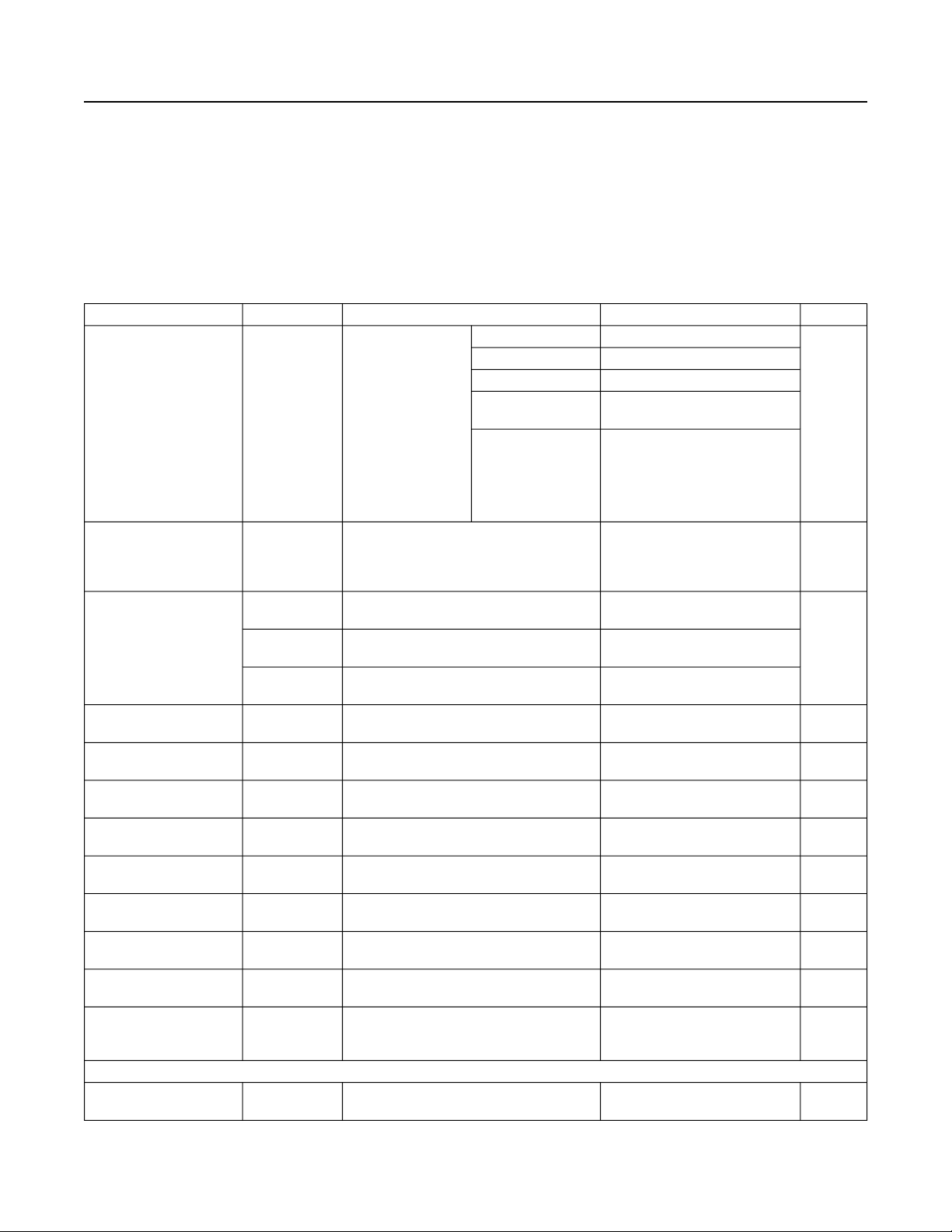
Electrical Characteristics (continued)
(Limits are 100% tested at TA= +25°C and TA= +105°C. TYP specifications are provided for TA= +25°C. Limits over the operating
temperature range and relevant supply voltage range are guaranteed by design and characterization. Specifications marked GBD are
guaranteed by design and not production tested. Specifications to the minimum operating temperature are guaranteed by design and
are not production tested. GPIO are only tested at TA= +105°C.)
PARAMETER SYMBOL CONDITIONS MIN TYP MAX UNITS
V
Current,
REGI
BACKUP Mode
V
Current, POWER
REGI
DOWN Mode
V
REGO_X
Output
Current
V
REGO_X
Output
Current Combined
V
REGO_X
Output
Voltage Range
V
REGO_X
Efficiency V
SLEEP Mode Resume
Time
LOW-POWER Mode
Resume Time
MICROPOWER Mode
Resume Time
STANDBY Mode
Resume Time
BACKUP Mode Resume
Time
POWER-DOWN Mode
Resume Time
CLOCKS
System Clock
Frequency
I
REGI_BK
I
REGI_PDM
V
REGO_A_IOU
T
V
REGO_B_IOU
T
V
REGO_C_IOU
T
V
REGO_X_IOU
T_TOT
V
REGO_X_RA
NGE
REGO_X_EFF
t
SLP_ON
t
LP_ON
t
MP_ON
t
STBY_ON
t
BKU_ON
t
PDM_ON
f
SYS_CLK
Total current into
V
pins, V
REGI
= 3.0V, V
V
COREB
REGI
COREA
= 1.1V,
RTC disabled, all
CNN quadrants
disabled, all CNN
memory disabled;
inputs tied to VSS,
V
, or V
DDIO
DDIOH
outputs source/sink
0mA
Total current into V
3.0V, V
COREA
tied to VSS, V
DDIO
source/sink 0mA
V
REGO_A
V
REGO_B
V
REGO_C
All three V
V
REGI
V
REGI
output current 5 50
output current 5 50
output current 10 100
REGO_X
≥ V
REGO_X
= 2.7V, V
30mA
Time from power mode exit to execution
of first user instruction
Time from power mode exit to execution
of first user instruction
Time from power mode exit to execution
of first user instruction
Time from power mode exit to execution
of first user instruction
Time from power mode exit to execution
of first user instruction
Time from power mode exit to execution
of first user instruction. Includes
bootloader execution time.
All SRAM retained 11.1
No SRAM retention 9
=
SRAM0 retained 9.6
SRAM0 and
SRAM1 retained
10.1
SRAM0, SRAM1,
= V
and SRAM2
;
retained
pins, V
REGI
COREB
, or V
DDIOH
=
REGI
= 1.1V; inputs
; outputs
10.6
0.17 μA
outputs combined 20 100 mA
+ 200mV 0.5 1.0 1.85 V
REGO_X
= 1.1 V, load =
90 %
0.67 μs
9.5 μs
31 us
35 μs
0.14 ms
5 ms
0.0625 100,000 kHz
μA
mA
www.maximintegrated.com
19-100868
Maxim Integrated | 11
Page 12
MAX78000 Ultra-Low-Power Arm Cortex-M4 Processor with
FPU-Based Microcontroller with Convolutional
Neural Network Accelerator
Electrical Characteristics (continued)
(Limits are 100% tested at TA= +25°C and TA= +105°C. TYP specifications are provided for TA= +25°C. Limits over the operating
temperature range and relevant supply voltage range are guaranteed by design and characterization. Specifications marked GBD are
guaranteed by design and not production tested. Specifications to the minimum operating temperature are guaranteed by design and
are not production tested. GPIO are only tested at TA= +105°C.)
PARAMETER SYMBOL CONDITIONS MIN TYP MAX UNITS
1/
System Clock Period t
Internal Primary
Oscillator (IPO)
Internal Secondary
Oscillator (ISO)
Internal Baud Rate
Oscillator (IBRO)
Internal Nano-Ring
Oscillator (INRO)
External RTC Oscillator
(ERTCO)
RTC Operating Current I
RTC Power-Up Time t
External I2S Clock Input
Frequency
External System Clock
Input Frequency
External Low Power
Timer 1 Clock Input
Frequency
External Low Power
Timer 2 Clock Input
Frequency
CONVOLUTIONAL NEURAL NETWORK
CNN Active Energy Ε
SYS_CLK
f
IPO
f
ISO
f
IBRO
f
INRO
f
ERTCO
RTC
RTC_ ON
f
EXT_I2S_CLK
f
EXT_CLK
f
EXT_LPTMR1_
CLK
f
EXT_LPTMR2_
CLK
J_CNN
8kHz selected 8
30kHz selected 32
32kHz watch crystal, CL= 6pF, ESR <
90kΩ, C0≤ 2pF
All power modes, RTC enabled 0.3 μA
I2S_CLKEXT selected 25 MHz
EXT_CLK selected 80 MHz
LPTMR1_CLK selected 8 MHz
LPTMR2_CLK selected 8 MHz
Max power
network, random
data, and random
mask configuration
x16 Quadrant 0, 1,
2, and 3 enabled
f
SYS_CL
K
100 MHz
60 MHz
7.3728 MHz
32.768 kHz
250 ms
4.02 pJ/MAC
ns
kHz16kHz selected 16
www.maximintegrated.com
19-100868
Maxim Integrated | 12
Page 13
MAX78000 Ultra-Low-Power Arm Cortex-M4 Processor with
FPU-Based Microcontroller with Convolutional
Neural Network Accelerator
Electrical Characteristics (continued)
(Limits are 100% tested at TA= +25°C and TA= +105°C. TYP specifications are provided for TA= +25°C. Limits over the operating
temperature range and relevant supply voltage range are guaranteed by design and characterization. Specifications marked GBD are
guaranteed by design and not production tested. Specifications to the minimum operating temperature are guaranteed by design and
are not production tested. GPIO are only tested at TA= +105°C.)
PARAMETER SYMBOL CONDITIONS MIN TYP MAX UNITS
x16 Quadrant 0
enabled; x16
Quadrant 1, 2, and
3 powered down
and isolated
x16 Quadrant 0, 1,
2, and 3 enabled
x16 Quadrant 0
enabled; x16
Quadrant 1, 2, and
3 powered down
and isolated
x16 Quadrant 0, 1,
2, and 3 enabled.
External power
supply must be
used for V
since the on-board
SIMO will not
supply above
100mA.
x16 Quadrant 0
enabled; x16
Quadrant 1, 2, and
3 powered down
and isolated
x16 Quadrant 0, 1,
2, and 3 enabled.
External power
supply must be
used for VCOREA
since the on-board
SIMO will not
supply above
100mA.
x16 Quadrant 0
only; x16 Quadrant
1, 2, and 3
powered down and
isolated
x16 Quadrant 0, 1,
2, and 3 enabled
COREA
10.1
29
31.7
118
mA
38.5
146
6.625
μA
26.5
V
Current
V
Retention Current
COREA
Mask Memory
REGI
CNN Active
I
COREA_CNN_
MNISTA
I
COREA_CNN_
MNISTB
I
COREA_CNNM
PRA
I
COREA_CNNM
PRB
I
COREA_CNNM
PA
I
COREA_CNNM
PB
I
REGI_CNNMRVCOREB
MNIST Standard
dataset, optimized
network
Max power
network, random
data, and random
mask configuration
Max power
network, data,
mask configuration
= 1.0V
www.maximintegrated.com
19-100868
Maxim Integrated | 13
Page 14
MAX78000 Ultra-Low-Power Arm Cortex-M4 Processor with
FPU-Based Microcontroller with Convolutional
Neural Network Accelerator
Electrical Characteristics (continued)
(Limits are 100% tested at TA= +25°C and TA= +105°C. TYP specifications are provided for TA= +25°C. Limits over the operating
temperature range and relevant supply voltage range are guaranteed by design and characterization. Specifications marked GBD are
guaranteed by design and not production tested. Specifications to the minimum operating temperature are guaranteed by design and
are not production tested. GPIO are only tested at TA= +105°C.)
PARAMETER SYMBOL CONDITIONS MIN TYP MAX UNITS
x16 Quadrant 0
enabled; x16
V
CNN Inactive
REGI
Current
GENERAL-PURPOSE I/O
Input Low Voltage for All
GPIO Except P3.0 and
P3.1
Input Low Voltage for All
GPIO
Input Low Voltage for
RSTN
Input High Voltage for
All GPIO Except P3.0
and P3.1
Input High Voltage for
All GPIO
Input High Voltage for
RSTN
CNN enabled/
I
REGI_CNNIA
V
IL_VDDIO
V
IL_VDDIOHVDDIOH
V
IL_RSTN
V
IH_VDDIO
V
IH_VDDIOHVDDIOH
V
IH_RSTN
inactive, clocks
disabled
P3.0 and P3.1 can
only use V
as I/O supply and
cannot use V
as I/O supply
P3.0 and P3.1 can
only use V
as I/O supply and
cannot use V
as I/O supply
Quadrant 1, 2, and
3 powered down
and isolated
x16 Quadrant 0, 1,
2, and 3 enabled
DDIOH
DDIO
selected as I/O supply
DDIOH
DDIO
selected as I/O supply
V
DDIO
I/O supply
V
DDIO
I/O supply
selected as
selected as
0.7 ×
V
DDIO
0.7 ×
V
DDIOH
264
790.4
0.5 x
V
DDIOH
0.5 x
V
DDIOH
0.3 ×
V
DDIO
0.3 ×
V
DDIOH
μA
V
V
V
V
V
V
www.maximintegrated.com
19-100868
Maxim Integrated | 14
Page 15
MAX78000 Ultra-Low-Power Arm Cortex-M4 Processor with
FPU-Based Microcontroller with Convolutional
Neural Network Accelerator
Electrical Characteristics (continued)
(Limits are 100% tested at TA= +25°C and TA= +105°C. TYP specifications are provided for TA= +25°C. Limits over the operating
temperature range and relevant supply voltage range are guaranteed by design and characterization. Specifications marked GBD are
guaranteed by design and not production tested. Specifications to the minimum operating temperature are guaranteed by design and
are not production tested. GPIO are only tested at TA= +105°C.)
PARAMETER SYMBOL CONDITIONS MIN TYP MAX UNITS
V
selected as
DDIO
Output Low Voltage for
All GPIO Except P3.0
and P3.1
Output Low Voltage for
All GPIO
Combined IOL, All GPIO I
V
OL_VDDIO
V
OL_VDDIOH
OL_TOTAL
I/O supply, V
= 1.71V,
GPIOn_DS_SEL[1:
0] = 00, IOL= 1mA
V
DDIO
I/O supply, V
P3.0 and P3.1 can
only use V
DDIOH
as I/O supply and
cannot use V
DDIO
as I/O supply
= 1.71V,
GPIOn_DS_SEL[1:
0] = 01, IOL= 2mA
V
DDIO
I/O supply, V
= 1.71V,
GPIOn_DS_SEL[1:
0] = 10, IOL= 4mA
V
DDIO
I/O supply, V
= 1.71V,
GPIOn_DS_SEL[1:
0] = 11, IOL= 8mA
V
selected as I/O supply, V
DDIOH
= 1.71V, GPIOn_DS_SEL[1:0] = 00, I
= 1mA
V
selected as I/O supply, V
DDIOH
= 1.71V, GPIOn_DS_SEL[1:0] = 01, I
= 2mA
V
selected as I/O supply, V
DDIOH
= 1.71V, GPIOn_DS_SEL[1:0] = 10, I
= 4mA
V
selected as I/O supply, V
DDIOH
= 1.71V, GPIOn_DS_SEL[1:0] = 11, I
= 8mA
DDIO
selected as
DDIO
selected as
DDIO
selected as
DDIO
DDIOH
OL
DDIOH
OL
DDIOH
OL
DDIOH
OL
0.2 0.4
0.2 0.4
V
0.2 0.4
0.2 0.4
0.2 0.4
0.2 0.4
V
0.2 0.4
0.2 0.4
48 mA
www.maximintegrated.com
19-100868
Maxim Integrated | 15
Page 16
MAX78000 Ultra-Low-Power Arm Cortex-M4 Processor with
FPU-Based Microcontroller with Convolutional
Neural Network Accelerator
Electrical Characteristics (continued)
(Limits are 100% tested at TA= +25°C and TA= +105°C. TYP specifications are provided for TA= +25°C. Limits over the operating
temperature range and relevant supply voltage range are guaranteed by design and characterization. Specifications marked GBD are
guaranteed by design and not production tested. Specifications to the minimum operating temperature are guaranteed by design and
are not production tested. GPIO are only tested at TA= +105°C.)
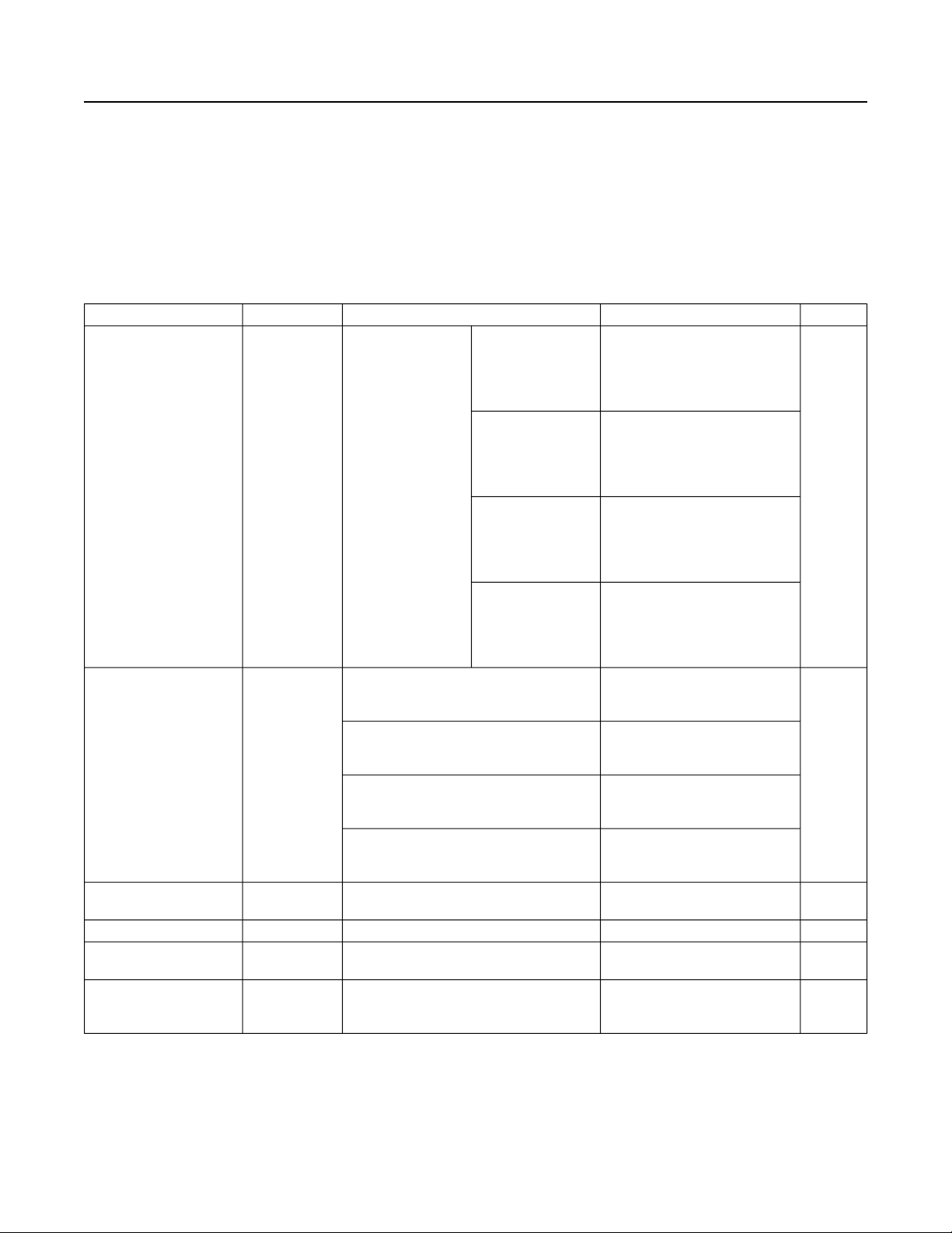
PARAMETER SYMBOL CONDITIONS MIN TYP MAX UNITS
V
selected as
DDIO
Output High Voltage for
All GPIO Except P3.0
and P3.1
Output High Voltage for
All GPIO Except P3.0
and P3.1
Output High Voltage for
P3.0 and P3.1
Combined IOH, All GPIO I
Input Hysteresis
(Schmitt)
Input Leakage Current
Low
V
OH_VDDIO
V
OH_VDDIOH
V
OH_VDDIOH
OH_TOTAL
V
IHYS
I
IL
I/O supply, V
= 1.71V,
GPIOn_DS_SEL[1:
0] = 00, IOL= -1mA
V
DDIO
I/O supply, V
P3.0 and P3.1 can
only use V
DDIOH
as I/O supply and
cannot use V
DDIO
as I/O supply
= 1.71V,
GPIOn_DS_SEL[1:
0] = 01, IOL= -2mA
V
DDIO
I/O supply, V
= 1.71V,
GPIOn_DS_SEL[1:
0] = 10, IOL= -4mA
V
DDIO
I/O supply, V
= 1.71V,
GPIOn_DS_SEL[1:
0] = 11, IOL= -8mA
V
selected as I/O supply, V
DDIOH
= 1.71V, GPIOn_DS_SEL[1:0] = 00, I
= -1mA
V
selected as I/O supply, V
DDIOH
= 1.71V, GPIOn_DS_SEL[1:0] = 01, I
= -2mA
V
selected as I/O supply, V
DDIOH
= 1.71V, GPIOn_DS_SEL[1:0] = 10, I
= -4mA
V
selected as I/O supply, V
DDIOH
= 1.71V, GPIOn_DS_SEL[1:0] = 11, I
= -8mA
V
= 1.71V, GPIOn_DS_SEL[1:0]
DDIOH
fixed at 00, IOL= -1mA
V
DDIO
= 1.89V, V
DDIOH
= 3.6V, V
selected as I/O supply, VIN= 0V, internal
pullup disabled
DDIO
selected as
DDIO
selected as
DDIO
selected as
DDIO
DDIOH
OL
DDIOH
OL
DDIOH
OL
DDIOH
OL
DDIOH
V
-
DDIO
0.4
V
-
DDIO
0.4
V
-
DDIO
0.4
V
-
DDIO
0.4
V
DDIOH
- 0.4
V
DDIOH
- 0.4
V
DDIOH
- 0.4
V
DDIOH
- 0.4
V
DDIOH
- 0.4
-48 mA
300 mV
-100 +100 nA
V
V
V
www.maximintegrated.com
19-100868
Maxim Integrated | 16
Page 17
MAX78000 Ultra-Low-Power Arm Cortex-M4 Processor with
FPU-Based Microcontroller with Convolutional
Neural Network Accelerator
Electrical Characteristics (continued)
(Limits are 100% tested at TA= +25°C and TA= +105°C. TYP specifications are provided for TA= +25°C. Limits over the operating
temperature range and relevant supply voltage range are guaranteed by design and characterization. Specifications marked GBD are
guaranteed by design and not production tested. Specifications to the minimum operating temperature are guaranteed by design and
are not production tested. GPIO are only tested at TA= +105°C.)
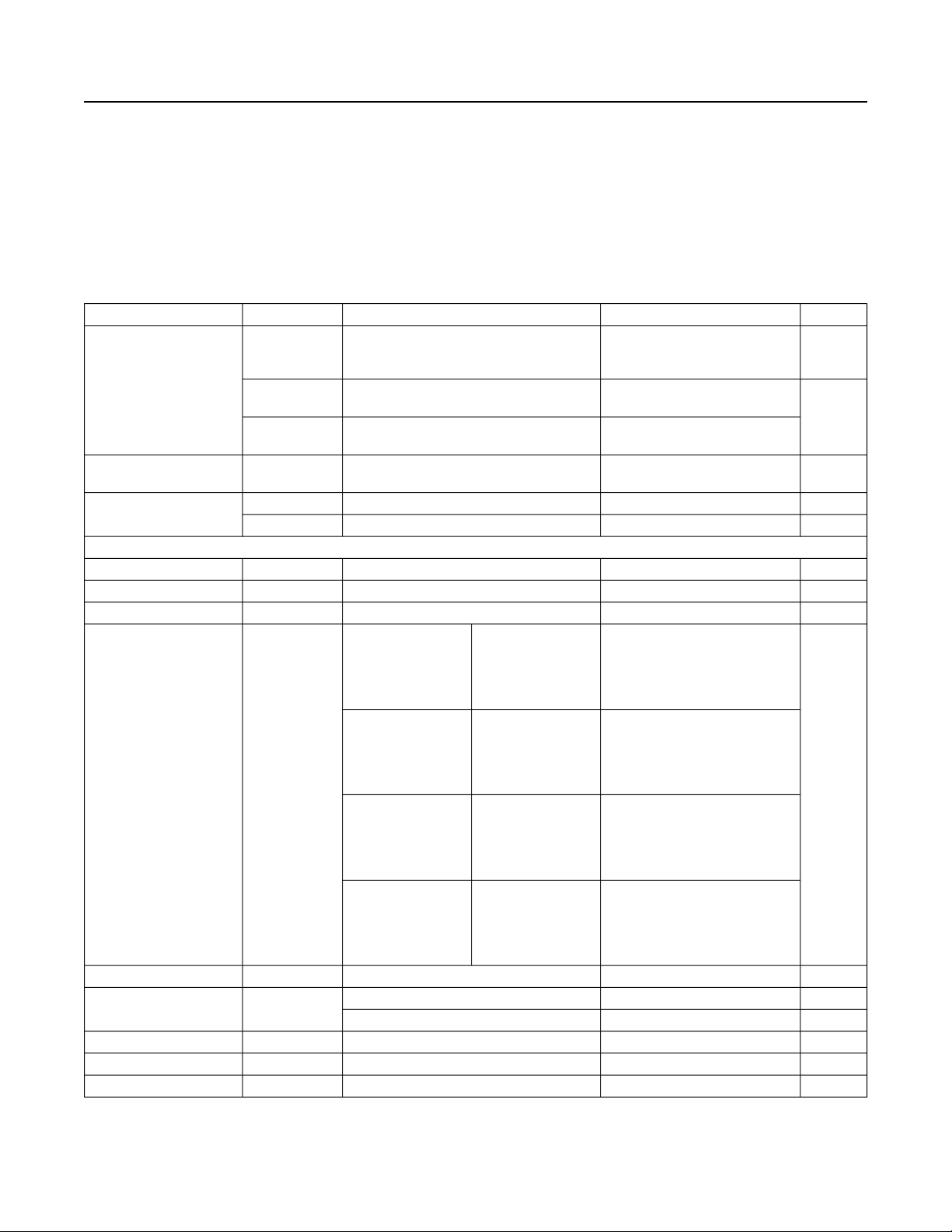
PARAMETER SYMBOL CONDITIONS MIN TYP MAX UNITS
V
= 1.89V, V
I
IH
DDIO
selected as I/O supply, VIN= 3.6V,
internal pulldown disabled
Input Leakage Current
High
Input Pullup Resistor
RSTN
Input Pullup/Pulldown
Resistor for All GPIO
I
I
R
R
R
OFF
IH3V
PU_R
PU1
PU2
V
= 0V, V
DDIO
DDIOH
selected as I/O supply, VIN< 1.89V
V
= V
DDIO
DDIOH
selected as I/O supply, VIN= 3.6V
Pullup to V
DDIOH
Normal resistance, P1M = 0 25 kΩ
Highest resistance, P1M = 1 1 MΩ
ADC (SIGMA-DELTA)
Resolution 10 Bits
ADC Clock Rate f
ADC Clock Period t
ACLK
ACLK
AIN[7:0],
ADC_DIVSEL =
[00],
ADC_CH_SEL =
[7:0]
AIN[7:0],
ADC_DIVSEL =
[01],
ADC_CH_SEL =
Input Voltage Range V
AIN
[7:0]
AIN[7:0],
ADC_DIVSEL =
[10],
ADC_CH_SEL =
[7:0]
AIN[7:0],
ADC_DIVSEL =
[11],
ADC_CH_SEL =
[7:0]
Input Impedance R
Analog Input
Capacitance
AIN
C
AIN
Fixed capacitance to V
Dynamically switched capacitance 250 fF
Integral Nonlinearity INL Measured at +25°C ±2 LSb
Differential Nonlinearity DNL Measured at +25°C ±1 LSb
Offset Error V
OS
= 3.6V, V
DDIOH
= 0V, V
DDIO
= 1.71V, V
DDIO
REF_SEL = 0,
INPUT_SCALE = 0
REF_SCALE = 0,
INPUT_SCALE = 0
REF_SCALE = 0,
INPUT_SCALE =
0, V
DDIOH
as the I/O supply
REF_SEL = 0,
INPUT_SCALE =
0, V
DDIOH
as the I/O supply
SSA
DDIOH
selected
selected
-800 +800 nA
-1 +1
-2 +2
25 kΩ
0.1 8 MHz
1/f
ACLK
V
+
V
V
V
SSA
0.05
SSA
0.05
SSA
0.05
SSA
0.05
+
+
+
V
2 x V
V
DDIOH
V
DDIOH
BG
BG
30 kΩ
1 pF
±1 LSb
μA
μs
V
www.maximintegrated.com
19-100868
Maxim Integrated | 17
Page 18
MAX78000 Ultra-Low-Power Arm Cortex-M4 Processor with
FPU-Based Microcontroller with Convolutional
Neural Network Accelerator
Electrical Characteristics (continued)
(Limits are 100% tested at TA= +25°C and TA= +105°C. TYP specifications are provided for TA= +25°C. Limits over the operating
temperature range and relevant supply voltage range are guaranteed by design and characterization. Specifications marked GBD are
guaranteed by design and not production tested. Specifications to the minimum operating temperature are guaranteed by design and
are not production tested. GPIO are only tested at TA= +105°C.)
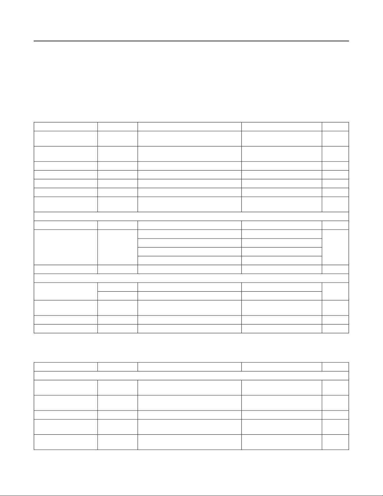
PARAMETER SYMBOL CONDITIONS MIN TYP MAX UNITS
ADC Active Current I
ADC Setup Time t
ADC Output Latency t
ADC Sample Rate f
ADC Input Leakage I
Full-Scale Voltage V
Bandgap Temperature
Coefficient
ADC
ADC_SU
ADC
ADC
ADC_LEAK
FS
V
TEMPCO
COMPARATORS
Input Offset Voltage V
Input Hysteresis V
Input Voltage Range V
OFFSET
HYST
IN_CMP
FLASH MEMORY
t
Flash Erase Time
Flash Programming
Time per Word
M_ERASE
t
P_ERASE
t
PROG
Flash Endurance 10 kcycles
Data Retention t
RET
ADC active, reference buffer enabled,
input buffer disabled
Any power-up of ADC clock or ADC bias
to CpuAdcStart
102 µA
10 µs
1067 t
ACLK
7.8 ksps
ADC inactive or channel not selected 10 nA
ADC code = 0x3FF 1.2 V
Box method 30 ppm
±1 mV
AINCOMPHYST[1:0] = 00 ±23
AINCOMPHYST[1:0] = 01 ±50
AINCOMPHYST[1:0] = 10 ±2
mV
AINCOMPHYST[1:0] = 11 ±7
Common-mode range 0.6 1.35 V
Mass erase 20
Page erase 20
32-bit programming mode, f
1MHz
FLC_CLK
=
42 μs
ms
TA= +105°C 10 years
Electrical Characteristics—SPI
(Timing specifications are guaranteed by design and not production tested.)
PARAMETER SYMBOL CONDITIONS MIN TYP MAX UNITS
MASTER MODE
SPI Master Operating
Frequency for SPI0
SPI Master Operating
Frequency for SPI1
SPI Master SCK Period t
SCK Output PulseWidth High/Low
MOSI Output Hold Time
After SCK Sample Edge
www.maximintegrated.com
t
MCH
f
MCK0
f
MCK1
MCKX
, t
t
MOH
MCL
f
SYS_CLK
f
SYS_CLK
f
SYS_CLK
f
SYS_CLK
= 100MHz, f
/2
= 100MHz, f
/4
19-100868
MCK0(MAX)
MCK1(MAX)
=
=
1/f
MCKX
t
/2 ns
MCKX
t
/2 ns
MCX
50 MHz
25 MHz
Maxim Integrated | 18
ns
Page 19
MAX78000 Ultra-Low-Power Arm Cortex-M4 Processor with
FPU-Based Microcontroller with Convolutional
Neural Network Accelerator
Electrical Characteristics—SPI (continued)
(Timing specifications are guaranteed by design and not production tested.)
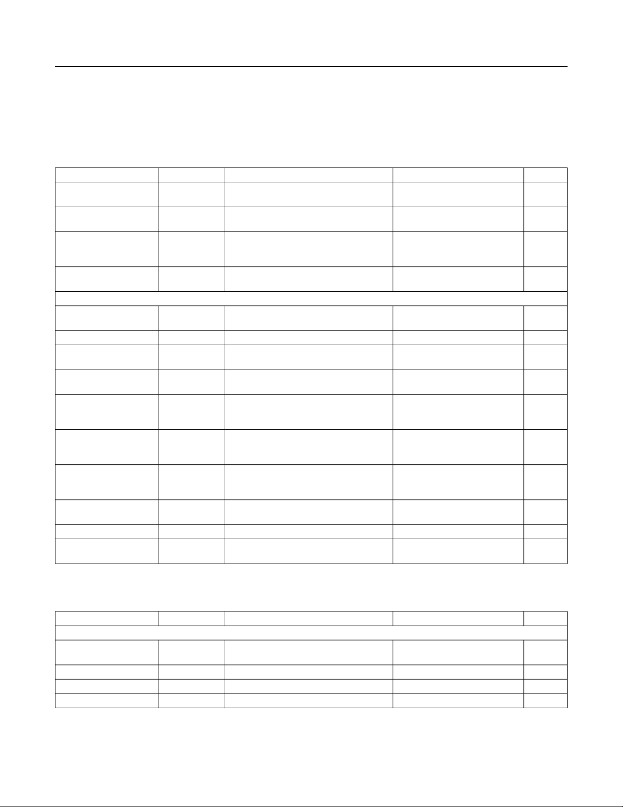
PARAMETER SYMBOL CONDITIONS MIN TYP MAX UNITS
MOSI Output Valid to
Sample Edge
MOSI Output Hold Time
After SCK Low Idle
MISO Input Valid to
SCK Sample Edge
Setup
MISO Input to SCK
Sample Edge Hold
SLAVE MODE
SPI Slave Operating
Frequency
SPI Slave SCK Period t
SCK Input Pulse-Width
High/Low
SSx Active to First Shift
Edge
MOSI Input to SCK
Sample Edge Rise/Fall
Setup
MOSI Input from SCK
Sample Edge Transition
Hold
MISO Output Valid After
SCLK Shift Edge
Transition
SCK Inactive to SSx
Inactive
SSx Inactive Time t
MISO Hold Time After
SSx Deassertion
t
SCH
t
MOV
t
MLH
t
MIS
t
MIH
f
SCK
SCK
t
SSE
t
SIS
t
SIH
t
SOV
t
SSD
SSH
t
SLH
t
/2 ns
MCKX
t
/2 ns
MCKX
5 ns
t
/2 ns
MCKX
50 MHz
1/f
SCK
, t
SCL
t
SCK
/2
ns
10 ns
5 ns
1 ns
5 ns
10 ns
1/f
SCK
μs
10 ns
Electrical Characteristics—I2C
(Timing specifications are guaranteed by design and not production tested.)
PARAMETER SYMBOL CONDITIONS MIN TYP MAX UNITS
STANDARD MODE
Output Fall Time t
SCL Clock Frequency f
Low Period SCL Clock t
High Time SCL Clock t
www.maximintegrated.com
OF
SCL
LOW
HIGH
Standard mode, from V
V
IL(MAX)
19-100868
IH(MIN)
to
150 ns
0 100 kHz
4.7 μs
4.0 μs
Maxim Integrated | 19
Page 20
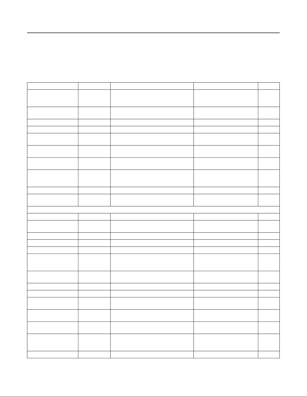
MAX78000 Ultra-Low-Power Arm Cortex-M4 Processor with
FPU-Based Microcontroller with Convolutional
Neural Network Accelerator
Electrical Characteristics—I2C (continued)
(Timing specifications are guaranteed by design and not production tested.)
PARAMETER SYMBOL CONDITIONS MIN TYP MAX UNITS
Setup Time for
Repeated Start
Condition
Hold Time for Repeated
Start Condition
Data Setup Time t
Data Hold Time t
Rise Time for SDA and
SCL
Fall Time for SDA and
SCL
Setup Time for a Stop
Condition
Bus Free Time Between
a Stop and Start
Condition
Data Valid Time t
Data Valid Acknowledge
Time
FAST MODE
Output Fall Time t
Pulse Width Suppressed
by Input Filter
SCL Clock Frequency f
Low Period SCL Clock t
High Time SCL Clock t
Setup Time for
Repeated Start
Condition
Hold Time for Repeated
Start Condition
Data Setup Time t
Data Hold Time t
Rise Time for SDA and
SCL
Fall Time for SDA and
SCL
Setup Time for a Stop
Condition
Bus Free Time Between
a Stop and Start
Condition
Data Valid Time t
t
SU;STA
t
HD;STA
SU;DAT
HD;DAT
t
R
t
F
t
SU;STO
t
BUS
VD;DAT
t
VD;ACK
OF
t
SP
SCL
LOW
HIGH
t
SU;STA
t
HD;STA
SU;DAT
HD;DAT
t
R
t
F
t
SU;STO
t
BUS
VD;DAT
From V
IH(MIN)
to V
IL(MAX)
4.7 μs
4.0 μs
300 ns
10 ns
800 ns
200 ns
4.0 μs
4.7 μs
3.45 μs
3.45 μs
150 ns
75 ns
0 400 kHz
1.3 μs
0.6 μs
0.6 μs
0.6 μs
125 ns
10 ns
30 ns
30 ns
0.6 μs
1.3 μs
0.9 μs
www.maximintegrated.com
19-100868
Maxim Integrated | 20
Page 21
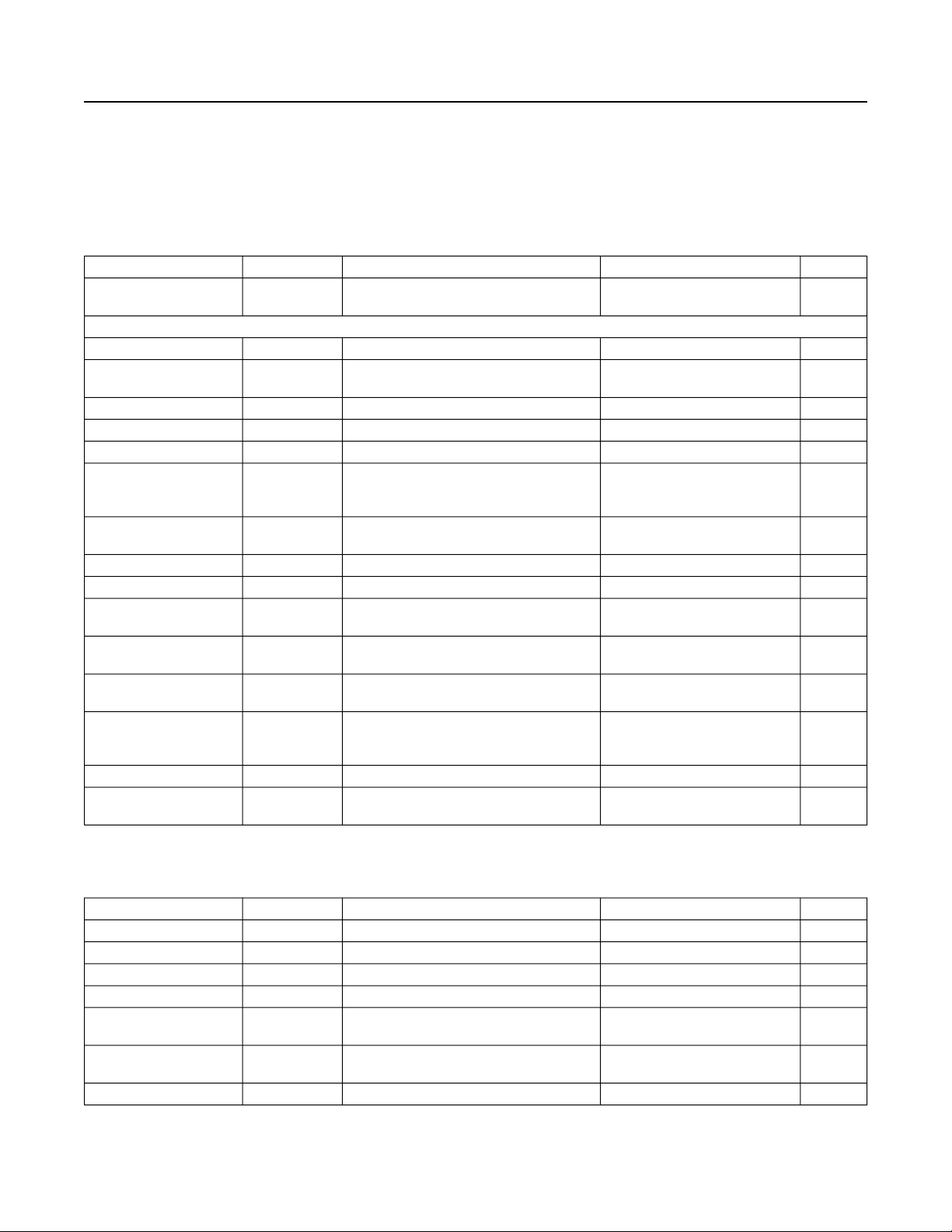
MAX78000 Ultra-Low-Power Arm Cortex-M4 Processor with
FPU-Based Microcontroller with Convolutional
Neural Network Accelerator
Electrical Characteristics—I2C (continued)
(Timing specifications are guaranteed by design and not production tested.)
PARAMETER SYMBOL CONDITIONS MIN TYP MAX UNITS
Data Valid Acknowledge
Time
FAST MODE PLUS
Output Fall Time t
Pulse Width Suppressed
by Input Filter
SCL Clock Frequency f
Low Period SCL Clock t
High Time SCL clock t
Setup Time for
Repeated Start
Condition
Hold Time for Repeated
Start Condition
Data Setup Time t
Data Hold Time t
Rise Time for SDA and
SCL
Fall Time for SDA and
SCL
Setup Time for a Stop
Condition
Bus Free Time Between
a Stop and Start
Condition
Data Valid Time t
Data Valid Acknowledge
Time
t
VD;ACK
OF
t
SP
SCL
LOW
HIGH
t
SU;STA
t
HD;STA
SU;DAT
HD;DAT
t
R
t
F
t
SU;STO
t
BUS
VD;DAT
t
VD;ACK
From V
IH(MIN)
to V
IL(MAX)
0.9 μs
80 ns
75 ns
0 1000 kHz
0.5 μs
0.26 μs
0.26 μs
0.26 μs
50 ns
10 ns
50 ns
30 ns
0.26 μs
0.5
μs
0.45 μs
0.45 μs
Electrical Characteristics—I2S
(Timing specifications are guaranteed by design and not production tested.)
PARAMETER SYMBOL CONDITIONS MIN TYP MAX UNITS
Bit Clock Frequency f
BCLK High Time t
BCLK
WBCLKH
0.5 1/f
BCLK Low Time 0.5 1/f
LRCLK Setup Time t
Delay Time, BCLK to
SD (Output) Valid
Setup Time for SD
(Input)
Hold Time SD (Input) t
www.maximintegrated.com
LRCLK_BLCK
t
BCLK_SDO
t
SU_SDI
HD_SDI
19-100868
25 ns
12 ns
6 ns
3 ns
25 MHz
Maxim Integrated | 21
BCLK
BCLK
Page 22
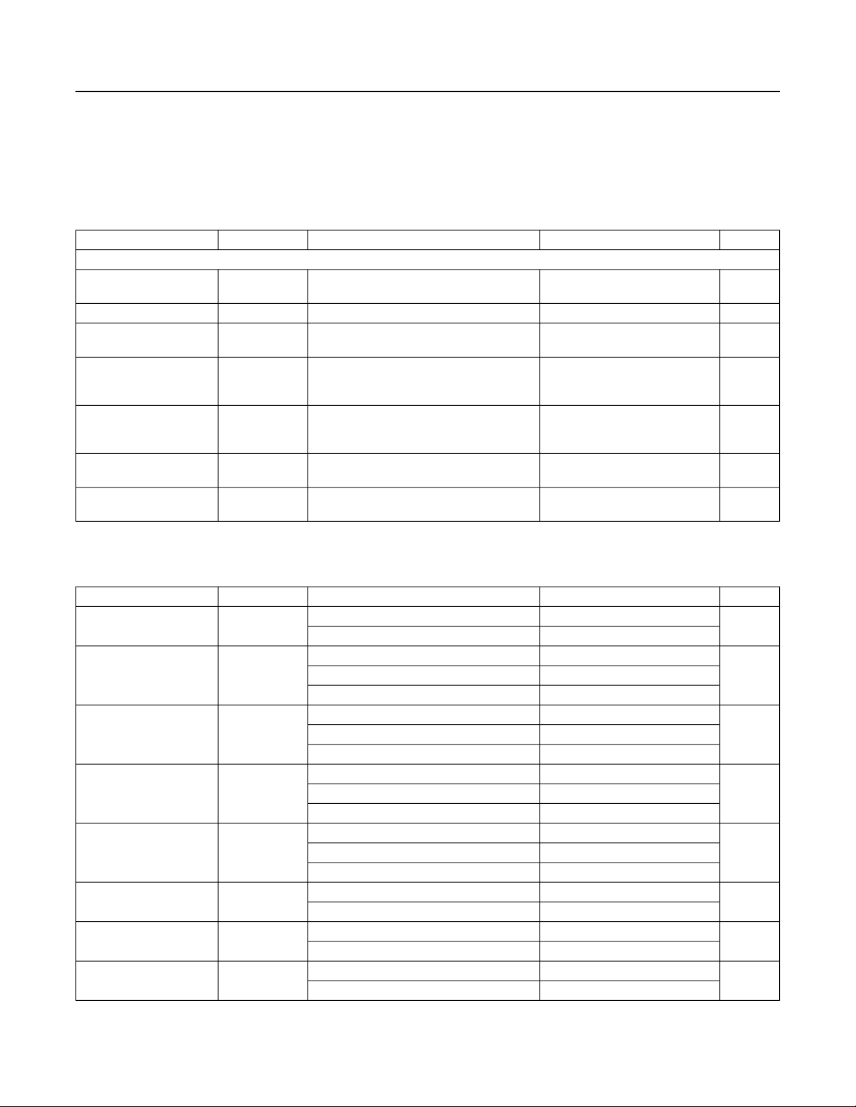
MAX78000 Ultra-Low-Power Arm Cortex-M4 Processor with
FPU-Based Microcontroller with Convolutional
Neural Network Accelerator
Electrical Characteristics—PCIF
(Timing specifications are guaranteed by design and not production tested.)
PARAMETER SYMBOL CONDITIONS MIN TYP MAX UNITS
PCIF
PCIF Operating
Frequency
PCIF Clock Period t
PCIF_PCLK Output
Pulse-Width High/Low
PCIF_VSYNC,
PCIF_HSYNC Setup
Time
PCIF_VSYNC,
PCIF_HSYNC Hold
Time
PCIF_D0-PCIF_D11
Setup TIme
PCIF_D0_PCIF_D11
Hold Time
t
WCH
f
CLK
CLK
t
SSU
t
SHLD
t
DSU
t
DHLD
, t
WCL
10 MHz
1/f
CLK
t
/2 ns
CLK
5 ns
5 ns
5 ns
5 ns
ns
Electrical Characteristics—1-Wire Master
(Timing specifications are guaranteed by design and not production tested.)
PARAMETER SYMBOL CONDITIONS MIN TYP MAX UNITS
Write 0 Low Time t
Write 1 Low Time t
Presence Detect
Sample
Read Data Value t
Recovery Time t
Reset Time High t
Reset Time Low t
Time Slot t
W0L
W1L
t
MSP
MSR
REC0
RSTH
RSTL
SLOT
Standard 60
Overdrive 8
Standard 6
Overdrive 1
Standard 70
Overdrive 9
Standard 15
Overdrive 3
Standard 10
Overdrive 4
Standard 480
Overdrive 58
Standard 600
Overdrive 70
Standard 70
Overdrive 12
μs
μsStandard, Long Line mode 8
μsStandard, Long Line mode 85
μsStandard, Long Line mode 24
μsStandard, Long Line mode 20
μs
μs
μs
www.maximintegrated.com
19-100868
Maxim Integrated | 22
Page 23
MAX78000 Ultra-Low-Power Arm Cortex-M4 Processor with
FPU-Based Microcontroller with Convolutional
Neural Network Accelerator
SHIFT SAMPLE SHIFT SAMPLE
SSx
(SHOWN ACTIVE LOW)
t
SCK
CKPOL/CKPHA
0/1 OR 1/0
SCK
CKPOL/CKPHA
0/0 OR 1/1
MOSI/SDIOx
(OUTPUT)
MISO/SDIOx
(INPUT)
MCK
t
MCH
t
t
MOH
MCL
t
MSB MSB-1
t
MIS
MSB MSB-1
MOV
t
MIH
LSB
LSB
t
MLH
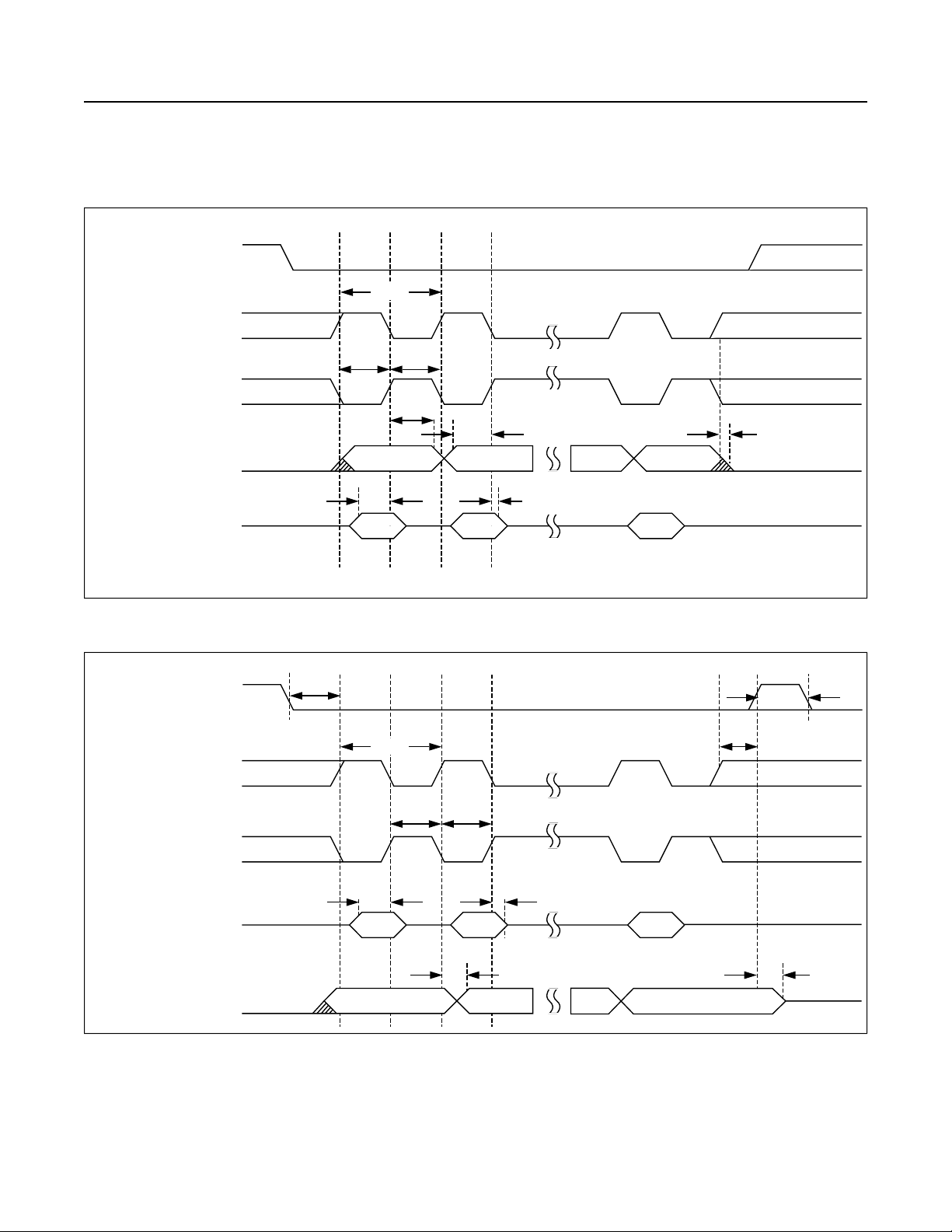
Figure 1. SPI Master Mode Timing Diagram
t
SSx
SSE
(SHOWN ACTIVE LOW)
SCK
CKPOL/CKPHA
0/1 OR 1/0
SCK
CKPOL/CKPHA
0/0 OR 1/1
MOSI/SDIOx
(INPUT)
MISO/SDIOx
(OUTPUT)
Figure 2. SPI Slave Mode Timing Diagram
SHIFT SAMPLE SHIFT SAMPLE
t
SCK
t
SCHtSCL
t
SIS
MSB MSB-1
t
SOV
MSB MSB-1
t
SIH
LSB
LSB
t
SSD
t
SSH
t
SLH
www.maximintegrated.com
19-100868
Maxim Integrated | 23
Page 24
MAX78000 Ultra-Low-Power Arm Cortex-M4 Processor with
FPU-Based Microcontroller with Convolutional
Neural Network Accelerator
START
SDA
t
OF
SCL
t
HD;STA
Figure 3. I2C Timing Diagram
BCLK
LRCLK
t
HD;DAT
t
VD;DAT
t
R
t
SU;DAT
t
LRCLK_BCLK
t
SU;STA
t
VD;ACK
START
REPEAT
STOP
t
BUS
t
t
SP
t
HIGH
SU;STO
t
LOW
t
BLK
t
WBCLKHtWBCLKL
START
t
SD
(OUTPUT)
SD
(INPUT)
WORD N-1 RIGHT CHANNEL WORD N LEFT CHANNEL WORD N RIGHT CHANNEL
Figure 4. I2S Timing Diagram
www.maximintegrated.com
BCLK_SDO
LSB MSB
LSB MSB
CONDITIONS: I2S_LJ = 0; I2S_MONO = 0;
CPOL = 0; CPHA = 0
19-100868
t
SU_SDI
t
HD_SDI
LSB MSB
LSB MSB
Maxim Integrated | 24
Page 25
MAX78000 Ultra-Low-Power Arm Cortex-M4 Processor with
FPU-Based Microcontroller with Convolutional
Neural Network Accelerator
t
CLK
t
WCHtWCL
PCIF_PCLK
t
SHLD
t
SSU
PCIF_VSYNC,
PCIF_HSYNC
t
DHLD
t
DSU
PCIF_D0—
PCIF_D11
Figure 5. Parallel Camera Interface Timing Diagram
Not
Valid
Not
Valid
www.maximintegrated.com
19-100868
Maxim Integrated | 25
Page 26
MAX78000 Ultra-Low-Power Arm Cortex-M4 Processor with
FPU-Based Microcontroller with Convolutional
Neural Network Accelerator
Figure 6. 1-Wire Master Data Timing Diagram
www.maximintegrated.com
19-100868
Maxim Integrated | 26
Page 27
MAX78000 Ultra-Low-Power Arm Cortex-M4 Processor with
FPU-Based Microcontroller with Convolutional
Neural Network Accelerator
Pin Configuration
81 CTBGA
TOP VIEW
1 2 3 4 5 6 7 8 9
MAX78000
A
B
C
D
E
F
G
H
V
SS
P1.8
P1.6 P1.9 P3.1 RSTN 32KIN LXA
V
V
DDIOH
V
COREA
DDIO
P1.7 P3.0 V
P1.4 P1.5 P0.21 P0.16 P0.11 P2.0
P1.3 P0.26 P0.20 P0.15 P0.10 P2.2 P2.1
P1.1 P1.2 P0.25 P0.19 P0.14 P0.9 P2.5 P2.4 P2.3
P1.0 P0.31 P0.24 P0.18 P0.13 P0.8 P0.6 P2.6 P2.7
P0.30 P0.28 P0.23 P0.17 P0.12 P0.7 P0.5 P0.3 P0.1
V
DDIOH
V
DDIO
V
SS
32KOUT
SS
V
SS
V
SSA
V
REGI
V
REGO_B
V
REGO_C
V
LXB
V
REGO_A
V
V
BST
COREB
DDA
V
V
V
SSPWR
REGI
COREA
V
SS
A
B
C
D
E
F
G
H
J
P0.29 P0.27 P0.22 P0.4 P0.2 P0.0
www.maximintegrated.com
V
DDIOH
V
DDIO
V
SS
1 2 3 4 5 6 7 8 9
81 CTBGA81 CTBGA
8mm X 8mm8mm X 8mm
19-100868
J
Maxim Integrated | 27
Page 28
MAX78000 Ultra-Low-Power Arm Cortex-M4 Processor with
FPU-Based Microcontroller with Convolutional
Neural Network Accelerator
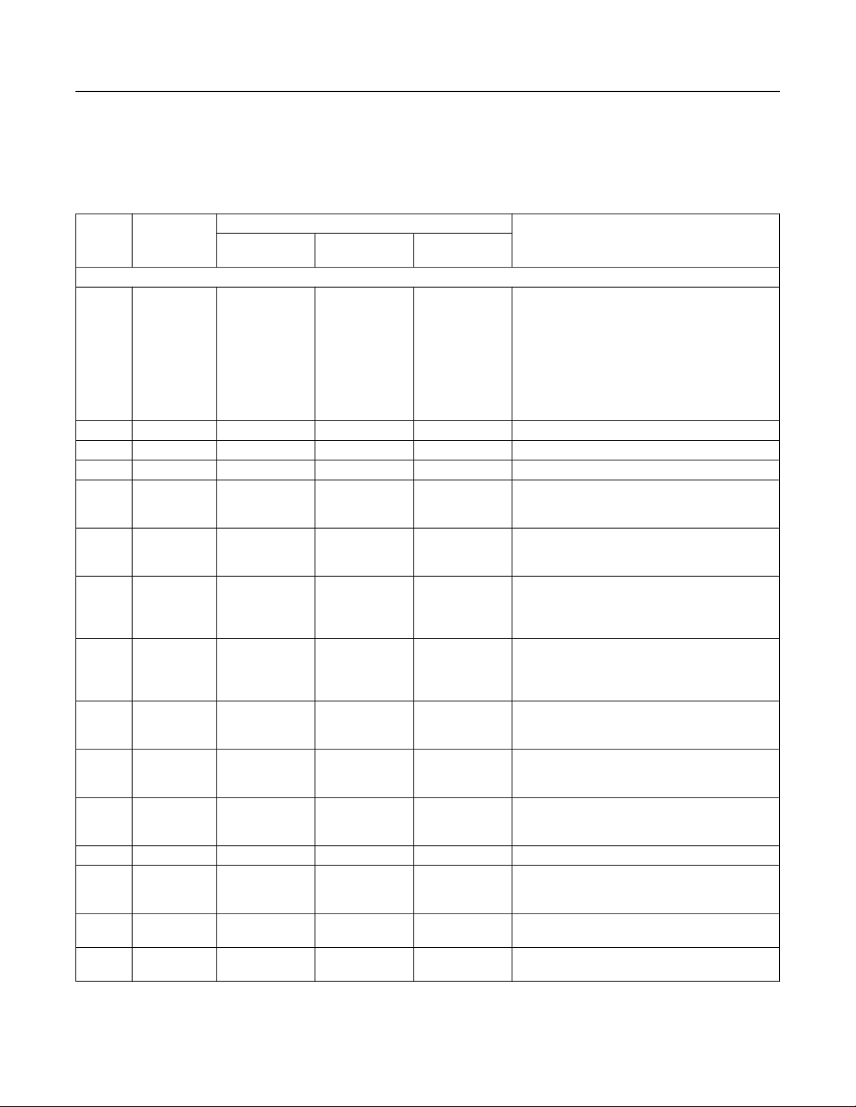
Pin Description
FUNCTION MODE
PIN NAME
Primary Signal
(Default)
Alternate
Function 1
Alternate
Function 2
POWER (See the Applications Information section for bypass capacitor recommendations.)
Battery Power Supply for the SIMO Switchmode
Power Supply (SMPS). Bypass device pin C9
with 2 x 47μF capacitors placed as close as
possible to the device pin C9 and V
C9, C6 V
REGI
— — —
for applications using a coin cell as the battery.
See Bypass Capacitors for more information. If
power to the device is cycled, the voltage
applied to this device pin must reach
V
REGI_POR
C7 V
D9, E1 V
D8 V
DDA
COREA
COREB
— — — 1.8V Analog Power Supply
— — — Digital Core Supply Voltage A
— — — Digital Core Supply Voltage B
Boosted Supply Voltage for the Gate Drive of
C8 V
BST
— — —
High-Side Switches. Bypass V
3.3nF capacitor.
Buck Converter A Voltage Output. Bypass
B8 V
REGO_A
— — —
V
REGO_A
with a 22μF capacitor to VSSplaced
as close as possible to the V
Buck Converter B Voltage Output. Bypass
A7 V
REGO_B
— — —
V
REGO_B
as close as possible to the closest V
with a 22μF capacitor to VSSplaced
device pin.
Buck Converter C Voltage Output. Bypass
B7 V
REGO_C
— — —
V
REGO_C
as close as possible to the closest V
with a 22μF capacitor to VSSplaced
device pin.
A4, D1,
J5
A3, C1,
J4
V
DDIO
V
DDIOH
— — —
— — —
GPIO Supply Voltage. Bypass this pin to V
with a 1.0μF capacitor placed as close as
possible to the package.
GPIO Supply Voltage, High. V
Bypass this pin to VSSwith a 1.0μF capacitor
placed as close as possible to the package.
A1, A6,
C4, C5,
V
SS
— — — Digital Ground
E9, J6
B6 V
SSA
— — — Analog Ground
Ground for the SIMO Switchmode Power Supply
A9 V
SSPWR
B9 LXA — — —
A8 LXB — — —
— — —
(SMPS). This device pin is the return path for
the V
REGI
Switching Inductor Input A. Connect a 2.2μH
inductor between LXA and LXB.
Switching Inductor Input B. Connect a 2.2μH
inductor between LXA and LXB.
FUNCTION
.
BST
DDA
DDIOH
device pins C6 and C9.
SSPWR
to LXB with a
device pin.
COREB
COREA
SS
≥ V
DDIO
pins
.
www.maximintegrated.com
19-100868
Maxim Integrated | 28
Page 29
MAX78000 Ultra-Low-Power Arm Cortex-M4 Processor with
FPU-Based Microcontroller with Convolutional
Neural Network Accelerator
81 CTBGA
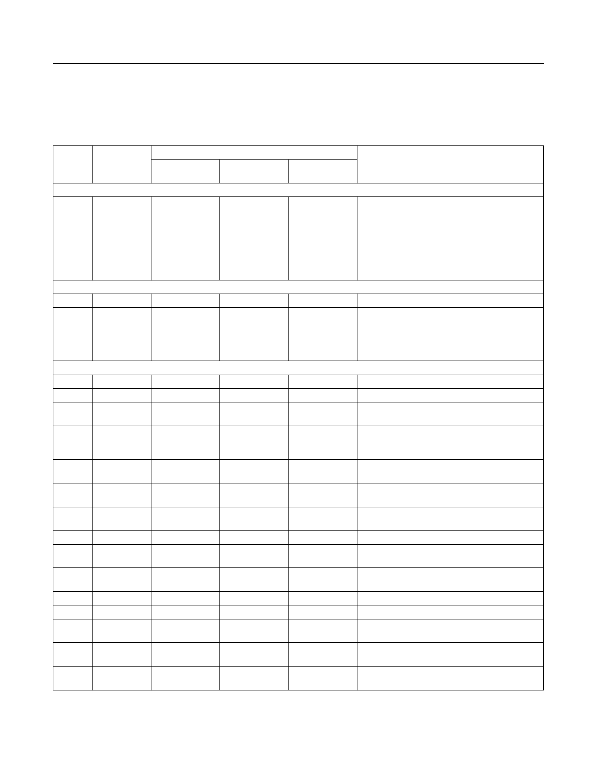
FUNCTION MODE
PIN NAME
RESET AND CONTROL
B4 RSTN — — —
CLOCK
A5 32KOUT — — — 32kHz Crystal Oscillator Output
B5 32KIN — — —
GPIO AND ALTERNATE FUNCTION (See the Applications Information section for GPIO and Alternate Function Matrices.)
J9 P0.0 P0.0 UART0A_RX — UART0 Receive Port Map A
H9 P0.1 P0.1 UART0A_TX — UART0 Transmit Port Map A
J8 P0.2 P0.2 TMR0A__IOA UART0B_CTS
H8 P0.3 P0.3
J7 P0.4 P0.4 SPI0_SS0 TMR0B_IOAN
H7 P0.5 P0.5 SPI0_MOSI TMR0B_IOBN
G7 P0.6 P0.6 SPI0_MISO OWM_IO
H6 P0.7 P0.7 SPI0_SCK OWM_PE SPI0 Clock; 1-Wire Master Pullup Enable Output
G6 P0.8 P0.8 SPI0_SDIO2 TMR0B_IOA
F6 P0.9 P0.9 SPI0_SDIO3 TMR0B_IOB
E6 P0.10 P0.10 I2C0_SCL SPI0_SS2 I2C0 Clock; SPI0 Slave Select 2
D6 P0.11 P0.11 I2C0_SDA SPI0_SS1 I2C0 Serial Data; SPI0 Slave Select 1
H5 P0.12 P0.12 UART1A_RX TMR1B_IOAN
G5 P0.13 P0.13 UART1A_TX TMR1B_IOBN
F5 P0.14 P0.14 TMR1A_IOA I2S_CLKEXT
Primary Signal
(Default)
Alternate
Function 1
EXT_CLK/
TMR0A_IOB
Alternate
Function 2
UART0B_RTS
Active-Low, External System Reset Input. The
device remains in reset while this pin is in its
active state. When the pin transitions to its
inactive state, the device performs a POR reset
(resetting all logic on all supplies except for RTC
circuitry) and begins execution.
This pin has an internal pullup to the V
supply.
32kHz Crystal Oscillator Input. Connect a 32kHz
crystal between 32KIN and 32KOUT for RTC
operation. Optionally, this pin can be configured
as the input for an external CMOS-level clock
source.
Timer 0 I/O 32 Bits or Lower 16 Bits Port Map A;
UART0 Clear to Send Port Map B
External Clock for Use as SYS_OSC/Timer 0
I/O Upper 16 Bits Port Map A; UART0 Request
to Send Port Map B
SPI0 Slave Select 0; Timer 0 Inverted Output
Port Map B
SP0 Master-Out Slave-In Serial Data 0; Timer 0
Inverted Output Upper 16 Bits Port Map B
SPI0 Master-In Slave-Out Serial Data 1; 1-Wire
Master Data I/O
SPI0 Data 2 I/O; Timer 0 I/O 32 Bits or Lower 16
Bits Port Map B
SPI0 Data 3 I/O; Timer 0 I/O Upper 16 Bits Port
Map B
UART1 Receive Port Map A; Timer 1 Inverted
Output Port Map B
UART1 Transmit Port Map A; Timer 1 Inverted
Output Upper 16 Bits Port Map B
Timer 1 I/O 32 Bits or Lower 16 Bits Port Map A;
I2S External Clock Input
FUNCTION
DDIOH
www.maximintegrated.com
19-100868
Maxim Integrated | 29
Page 30
MAX78000 Ultra-Low-Power Arm Cortex-M4 Processor with
FPU-Based Microcontroller with Convolutional
Neural Network Accelerator
81 CTBGA
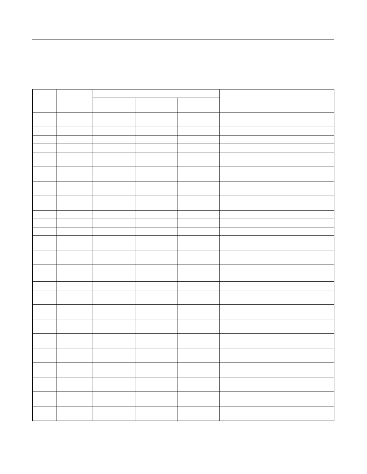
FUNCTION MODE
PIN NAME
E5 P0.15 P0.15 TMR1A_IOB PCIF_VSYNC
D5 P0.16 P0.16 I2C1_SCL PT2 I2C1 Clock; Pulse Train 2
H4 P0.17 P0.17 I2C1_SDA PT3 I2C1 Serial Data; Pulse Train 3
G4 P0.18 P0.18 PT0 OWM_IO Pule Train 0; 1-Wire Master Data I/O
F4 P0.19 P0.19 PT1 OWM_PE
E4 P0.20 P0.20 SPI1_SS0 PCIF_D0
D4 P0.21 P0.21 SPI1_MOSI PCIF_D1
J3 P0.22 P0.22 SPI1_MISO PCIF_D2
H3 P0.23 P0.23 SPI1_SCK PCIF_D3 SPI1 Clock; Parallel Camera Interface Data 3
G3 P0.24 P0.24 SPI1_SDIO2 PCIF_D4 SPI1 Data 2; Parallel Camera Interface Data 4
F3 P0.25 P0.25 SPI1_SDIO3 PCIF_D5 SPI1 Data 3; Parallel Camera Interface Data 5
E3 P0.26 P0.26 TMR2A_IOA PCIF_D6
J2 P0.27 P0.27 TMR2A_IOB PCIF_D7
H2 P0.28 P0.28 SWDIO — Serial Wire Debug Data I/O
J1 P0.29 P0.29 SWCLK — Serial Wire Debug Clock
H1 P0.30 P0.30 I2C2_SCL PCIF_D8 I2C2 Clock; Parallel Camera Interface Data 8
G2 P0.31 P0.31 I2C2_SDA PCIF_D9
G1 P1.0 P1.0 UART2A_RX RV_TCK
F1 P1.1 P1.1 UART2A_TX RV_TMS
F2 P1.2 P1.2 I2S_SCK RV_TDI
E2 P1.3 P1.3 I2S_WS RV_TDO
D2 P1.4 P1.4 I2S_SDI TMR3B_IOA
D3 P1.5 P1.5 I2S_SDO TMR3B_IOB
B1 P1.6 P1.6 TMR3A_IOA PCIF_D10
C2 P1.7 P1.7 TMR3A_IOB PCIF_D11
Primary Signal
(Default)
Alternate
Function 1
Alternate
Function 2
Timer 1 I/O Upper 16 Bits Port Map A; Parallel
Camera Interface Vertical Sync
Pulse Train 1; 1-Wire Master Pullup Enable
Output
SPI1 Slave Select 0; Parallel Camera Interface
Data 0
SPI1_Master Out Slave In Serial Data 0; Parallel
Camera Interface Data 1
SPI1 Master In Slave Out Serial Data 1; Parallel
Camera Interface Data 2
Timer 2 I/O 32 Bits or Lower 16 Bits Port Map A;
Parallel Camera Interface Data 6
Timer 2 I/O Upper 16 Bits Port Map A; Parallel
Camera Interface Data 7
I2C2 Serial Data; Parallel Camera Interface
Data 9
UART2 Receive Port Map A; 32-bit RISC-V Test
Port Clock
UART2 Transmit Port Map A; 32-bit RISC-V
Test Port Select
I2S Bit Clock; 32-bit RISC-V Test Port Data
Input
I2S Left/Right Clock; 32-bit RISC-V Test Port
Data Output
I2S Serial Data Input; Timer 3 I/O 32 Bits or
Lower 16 Bits Port Map B
I2S Serial Data Output; Timer 3 I/O Upper 16
Bits Port Map B
Timer 3 I/O 32 Bits or Lower 16 Bits Port Map A;
Parallel Camera Interface Data 10
Timer 3 I/O Upper 16 Bits Port Map A; Parallel
Camera Interface Data 11
FUNCTION
www.maximintegrated.com
19-100868
Maxim Integrated | 30
Page 31
MAX78000 Ultra-Low-Power Arm Cortex-M4 Processor with
FPU-Based Microcontroller with Convolutional
Neural Network Accelerator
81 CTBGA
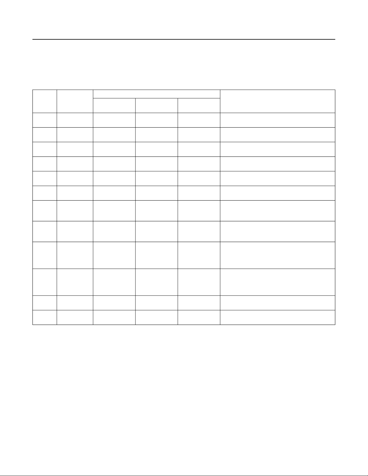
FUNCTION MODE
PIN NAME
A2 P1.8 P1.8 PCIF_HSYNC RXEV0
B2 P1.9 P1.9 PCIF_PCLK TXEV0
D7 P2.0 P2.0 AIN0/AINON —
E8 P2.1 P2.1 AIN1/AIN0P —
E7 P2.2 P2.2 AIN2/AIN1N —
F9 P2.3 P2.3 AIN3/AIN1P —
F8 P2.4 P2.4 AIN4/AIN2N LPTMR0B_IOA
F7 P2.5 P2.5 AIN5/AIN2P LPTMR1_IOA
G8 P2.6 P2.6
G9 P2.7 P2.7
C3 P3.0 P3.0 PDOWN WAKEUP
B3 P3.1 P3.1 SQWOUT WAKEUP
Primary Signal
(Default)
Alternate
Function 1
LPTMR0_CLK/
AIN6/AIN3N
LPTMR1_CLK/
AIN7/AIN3P
Alternate
Function 2
LPUARTB_RX
LPUARTB_TX
Parallel Camera Interface Horizontal Sync; CM4
RX Event Input
Parallel Camera Interface Pixel Clock; CM4 TX
Event Output
Analog to Digital Converter Input 0/Comparator
0 Negative Input
Analog to Digital Converter Input 1/Comparator
0 Positive Input
Analog to Digital Converter Input 2/Comparator
1 Negative Input
Analog to Digital Converter Input 3/Comparator
1 Positive Input
Analog to Digital Converter Input 4/Comparator
2 Negative Input; Low-Power Timer 0 I/O Port
Map B
Analog to Digital Converter Input 5/Comparator
2 Positive Input; Low-Power Timer 1 I/O Port
Map B
Low-Power Timer 0 External Clock Input/Analog
to Digital Converter Input 6/Comparator 3
Negative Input; Low-Power UART 0 Receive
Port Map B
Low-Power Timer 1 External Clock Input/Analog
to Digital Converter Input 7/Comparator 3
Positive Input; Low-Power UART Transmit Port
Map B
Power-Down Output; Wakeup Input. This device
pin can only be powered by V
Square-Wave Output; Wakeup Input. This
device pin can only be powered by V
FUNCTION
DDIOH
.
DDIOH
.
www.maximintegrated.com
19-100868
Maxim Integrated | 31
Page 32

MAX78000 Ultra-Low-Power Arm Cortex-M4 Processor with
FPU-Based Microcontroller with Convolutional
Neural Network Accelerator
Detailed Description
The MAX78000 is the first of a new breed of low-power microcontrollers built to thrive in the rapidly evolving AI at the edge
market. These products include Maxim's proven ultra-low power MCU IP along with deep neural network AI acceleration.
The MAX78000 is an advanced system-on-chip featuring an Arm®Cortex®-M4 with FPU CPU for efficient computation of
complex functions and algorithms with integrated power management. It also includes a 442KB-weight CNN accelerator.
The devices offer large on-chip memory with 512KB flash and up to 128KB SRAM. Multiple high-speed and lowpower communication interfaces are supported including high-speed SPI, high-speed I2C serial interface, and LPUART.
Additional low-power peripherals include flexible LPTIMER and analog comparators. A PCIF is included for capturing
images from an image sensor for processing by the CNN. An I2S interface is included for interfacing to an audio codec
for capturing audio samples also for processing by the CNN.
Arm Cortex-M4 with FPU Processor and RISC-V RV32 Processor
The Arm Cortex-M4 with FPU processor CM4 is ideal for the artificial intelligence system control. The architecture
combines high-efficiency signal processing functionality with low power, low cost, and ease of use.
The Arm Cortex-M4 with FPU DSP supports single instruction, multiple data (SIMD) path DSP extensions, providing:
● Four parallel 8-bit add/sub
● Floating point single precision
● Two parallel 16-bit add/sub
● Two parallel MACs
● 32- or 64-bit accumulate
● Signed, unsigned, data with or without saturation
The addition of a 32-bit RISC-V coprocessor RV32 provides the system with ultra-low power consumption signal
processing.
Convolutional Neural Network Accelerator (CNN)
The CNN accelerator consists of 64 parallel processors with 512KB of SRAM-based storage. Each processor includes a
pooling unit and a convolutional engine with dedicated weight memory. Four processors share one data memory. These
are further organized into groups of 16 processors that share common controls. A group of 16 processors operates as
a slave to another group or independently. Data is read from SRAM associated with each processor and written to any
data memory located within the accelerator. Any given processor has visibility of its dedicated weight memory and to the
data memory instance it shares with the three others.
The features of the CNN accelerator include:
● 512KB SRAM data storage
• Configured as 8Kx8-bit integers x64 channels or 32Kx8-bit integers x4 channels for input layers
• Hardware load and unload assist
● 64 parallel physical channel processors
• Organized as 4x16 processors
• 8-bit integer data path with option for 32-bit integers on the output layer
• Per-channel processor enable/disable
• Expandable to 1024 parallel logical channel processors
● 1x1 or 3x3 2D kernel sizes
● Configurable 1D kernel size to 1x9
● Full resolution sum-of-product arithmetic for 1024 8-bit integer channels
● Operating frequency up to 50MHz
● Nominal 1 output channel per clock, maximum 4 output channels per clock (passthru)
● Configurable input layer image size
www.maximintegrated.com
19-100868
Maxim Integrated | 32
Page 33

MAX78000 Ultra-Low-Power Arm Cortex-M4 Processor with
FPU-Based Microcontroller with Convolutional
Neural Network Accelerator
• 32K pixels, 16 channels, non-streaming
• 8K pixels, 4 channels, non-streaming
• 1024 x 1024 pixels, 4 channels, streaming
● Hidden layers
• Up to 8K 8-bit integer data per channel, x64 channels, non-streaming
• 8K bytes can be split equally across 1 to 16 logical channels, non-streaming
• 1M 8-bit integer data per channel, x64 channels, streaming
• 1M bytes can be split equally across eight layers, streaming
● Optional interrupt on CNN completion
● User-accessible BIST on all SRAM storage
● User-accessible zeroization of all SRAM storage
● Single-step operation with full data SRAM access for CNN operation debug
● Flexible power management
• Independent x16 processor supply enables
• Independent x16 processor mask retention enables
• Independent x16 data path clock enables
• Active Arm peripheral bus clock gating with per x16 processor override
• CNN clock frequency scaling (divide by 2, 4, 8, 16)
• Chip-level voltage control for performance power optimization
● Configurable weight storage
• SRAM-based weight storage with selectable data retention
• Configurable from 442K 8-bit integer weights to 3.456M 1-bit logical weights
• Organized as 768X9X64 8-bit integer weights to 768x72x64 1-bit logical weights
• Can be configured on a per-layer basis
• Programmable per x16 processor weight RAM start address, start pointer, and mask count
• Optional weight load hardware assist for packed weight storage
● 32 independently configurable layer groups
• Each group can contain element-wise, and/or pooling, and/or convolution operations for a minimum of 32 and a
maximum of 96 layers
• Processor and mask enables (16 channels)
• Input data format
• Per-layer data streaming
• Stream start - relative to prior stream
• Dual-stream processing delay counters - 1 column, 1 row delta counter
• Data SRAM circular buffer size
• Input data size (row, column)
• Row and column padding 0 to 4 bytes
• Number of input channels 1 to 1024
• Kernel bit width size (1, 2, 4, 8)
• Kernel SRAM start pointer and count
• Inflight input image pooling
• Pool mode - none, maximum or average
• Pool size - 1x1 to 16x16
• Stride - 1 row, 1 column to 4 rows, 4 columns
• Data SRAM read pointer base address
• Data SRAM write pointer configuration
• Base address
• Independent offsets for output channel storage in SRAM
• Programmable stride increment offset
• Bias - 2048 8-bit integers with option for 512 32-bit integers
• Pre-activation output scaling from 0 to 8 bits
www.maximintegrated.com
19-100868
Maxim Integrated | 33
Page 34

MAX78000 Ultra-Low-Power Arm Cortex-M4 Processor with
FPU-Based Microcontroller with Convolutional
Neural Network Accelerator
• Output activation - none, ReLU, absolute value
• Passthru - 8-bit or 32-bit integers
• Element-wise operations (add, subtract, xor, or) with optional convolution - up to 16 elements
• Deconvolution (upscaling)
• Flattening for MLP processing
• 1x1 convolution
Memory
Internal Flash Memory
512KB of internal flash memory provides nonvolatile storage of program and data memory.
Internal SRAM
The internal 128KB SRAM provides low-power retention of application information in all power modes except POWER
DOWN. The SRAM is divided into 4 banks. SRAM0 and SRAM1 are both 32KB, SRAM2 is 48KB and SRAM3 is 16KB.
SRAM2 and SRAM3 are accessible by the RV-32 in LOW POWER mode. For enhanced system reliability, SRAM0
(32KB) can be configured with error correction coded (ECC) single error correction-double error detection (SED-DED).
This data retention feature is optional and configurable. This granularity allows the application to minimize its power
consumption by only retaining the most essential data.
Comparators
The eight AIN[7:0] inputs can be configured as four pairs and deployed as four independent comparators with the
following features:
● Comparison events can trigger interrupts
● Events can wake the CM4 from SLEEP, LOW POWER, MICRO POWER, STANDBY, or BACKUP operating modes
● Can be active in all power modes
Dynamic Voltage Scaling (DVS) Controller
The DVS controller works using the fixed high-speed oscillator and the V
Arm core at the lowest practical voltage. The ability to adaptively adjust the voltage provides a significant reduction in
dynamic power consumption.
The DVS controller provides the following features:
● Controls DVS monitoring and adjustment functions
● Continuous monitoring with programmable monitor sample period
● Controlled transition to a programmable operating point
● Independent high and low operating limits for safe, bounded operation
● Independent high, center, and low operating range delay line delay monitors
● Programmable adjustment rate – when an adjustment is required
● Single clock operation
● Arm peripheral bus interface provides control and status access
● Interrupt capability during error
COREA
supply voltage to optimally operate the
Clocking Scheme
Multiple clock sources can be selected as the system clock:
● Internal primary oscillator (IPO) at a nominal frequency of 100MHz
● Internal secondary oscillator (ISO) at a nominal frequency of 60MHz
● Configurable internal nano-ring oscillator (INRO) at 8kHz, 16kHz, or 30kHz
● External RTC oscillator at 32.768kHz (ERTCO) (external crystal required)
● Internal baud rate oscillator at 7.3728MHz (IBRO)
www.maximintegrated.com
19-100868
Maxim Integrated | 34
Page 35
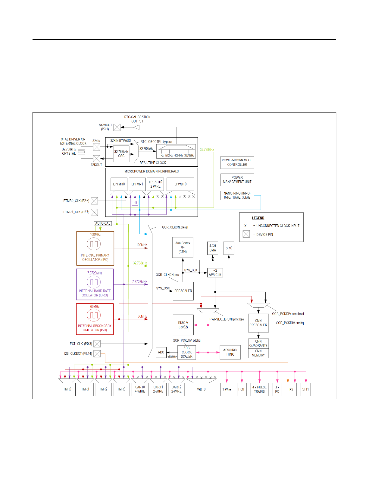
MAX78000 Ultra-Low-Power Arm Cortex-M4 Processor with
FPU-Based Microcontroller with Convolutional
Neural Network Accelerator
● External square-wave clock up to 80MHz
There are multiple external clock inputs:
● LPTMR0 and LPTMR1 can be clocked from unique external sources.
● I2S can be be clocked from its own external source.
Figure 7. Clocking Scheme Diagram
General-Purpose I/O and Special Function Pins
Most general-purpose I/O (GPIO) pins share both a firmware-controlled I/O function and one or more alternate functions
www.maximintegrated.com
19-100868
Maxim Integrated | 35
Page 36

MAX78000 Ultra-Low-Power Arm Cortex-M4 Processor with
FPU-Based Microcontroller with Convolutional
Neural Network Accelerator
associated with peripheral modules. Pins can be individually enabled for GPIO or peripheral special function use.
Configuring a pin as a special function usually supersedes its use as a firmware-controlled I/O. Although this multiplexing
between peripheral and GPIO functions is usually static, it can also be done dynamically. The electrical characteristics of
a GPIO pin are identical whether the pin is configured as an I/O or special function, except where explicitly noted in the
Electrical Characteristics tables.
In GPIO mode, pins are logically divided into ports of 32 pins. Each pin of a port has an interrupt function that can be
independently enabled, and configured as a level- or edge-sensitive interrupt. All GPIOs of a given port share the same
interrupt vector.
When configured as GPIO, the following features are provided. The features can be independently enabled or disabled
on a per-pin basis.
● Configurable as input, output, bidirectional, or high impedance
● Optional internal pullup resistor or internal pulldown resistor when configured as input
● Exit from low-power modes on rising or falling edge
● Selectable standard- or high-drive modes
The MAX78000 provides up to 52 GPIO pins. Caution is needed since Port 3 (P3.0 and P3.1 device pins) are configured
in a different manner from the above description.
Parallel Camera Interface (PCIF)
The PCIF is a low voltage interface suited for CMOS image sensors. It provides up to 12-bits of parallel access capability
with single capture and continuous mode operation.
Analog-to-Digital Converter
The 10-bit sigma-delta ADC provides an integrated reference generator and a single-ended input multiplexer. The
multiplexer selects an input channel from one of the eight external analog input signals (AIN0–AIN7) or the internal power
supply inputs.
The reference for the ADC can be:
● Internal 1.22V bandgap
● V
An optional feature allows samples captured by the ADC to be automatically compared against user-programmable high
and low limits. Up to four channel limit pairs can be configured in this way. The comparison allows the ADC to trigger an
interrupt (and potentially wake the CPU from a power mode) when a captured sample goes outside the preprogrammed
limit range. Since this comparison is performed directly by the sample limit monitors, it can be performed even while the
CPU is in SLEEP, LOW POWER or MICRO POWER mode. The eight AIN[7:0] inputs can be configured as four pairs
and deployed as four independent comparators.
The ADC measures the following voltages:
● AIN[7:0] up to 3.3V
● V
● V
● V
● V
● V
● V
analog supply
SSA
REGI
SSA
COREA
COREB
DDIOH
DDIO
Single-Inductor Multiple-Output Switch-Mode Power Supply (SIMO SMPS)
The SIMO SMPS built into the device provides a monolithic power supply architecture for operation from a single lithium
cell. The SIMO provides three buck regulator outputs that are voltage programmable. This architecture optimizes power
consumption efficiency of the device and minimizes the bill of materials for the circuit design since only a single inductor/
capacitor pair is required.
www.maximintegrated.com
19-100868
Maxim Integrated | 36
Page 37

MAX78000 Ultra-Low-Power Arm Cortex-M4 Processor with
FPU-Based Microcontroller with Convolutional
Neural Network Accelerator
Power Management
Power Management Unit
The power management unit (PMU) provides high-performance operation while minimizing power consumption. It
exercises intelligent, precise control of power distribution to the CPUs and peripheral circuitry.
The PMU provides the following features:
● User-configurable system clock
● Automatic enabling and disabling of crystal oscillators based on power mode
● Multiple power domains
● Fast wake-up of powered-down peripherals when activity detected
ACTIVE Mode
In this mode, the CM4 and the RV32 can execute application code and all digital and analog peripherals are available on
demand. Dynamic clocking disables peripherals not in use, providing the optimal mix of high performance and low power
consumption. The CM4 has access to all system SRAM. The RV32 has access to SRAM2 and SRAM3. Both the CM4
and the RV32 can execute from internal flash simultaneously. SRAM3 can be configured as an instruction cache for the
RV32.
SLEEP Mode
This mode consumes less power, but wakes faster because the clocks can optionally be enabled.
The device status is as follows:
● CM4 is asleep.
● RV32 is asleep.
● CNN quadrants and memory are configurable.
● Peripherals are on.
● Standard DMA is available for optional use.
LOW POWER Mode (LPM)
This mode is suitable for running the RV32 processor to collect and move data from enabled peripherals.
The device status is as follows:
● The CM4, SRAM0, SRAM1 are in state retention.
● CNN quadrants and memory are configurable and active.
● The RV32 can access the SPI, all UARTS, all timers, I2C, 1-Wire, pulse train engines, I2S, CRC, AES, TRNG, PCIF,
and comparators, as well as SRAM2 and SRAM3. SRAM3 can be configured to operate as RV32 instruction cache.
● The transition from LOW POWER mode to ACTIVE mode is faster than the transition from BACKUP mode because
system initialization is not required.
● The DMA can access flash.
● IPO can be optionally powered down.
● The following oscillators are enabled:
• IBRO
• ERTCO
• INRO
• ISO
MICRO POWER Mode (μPM)
This mode is used for extremely low power consumption while using a minimal set of peripherals to provide wakeup
capability.
The device status is as follows:
● Both CM4 and RV32 are state retained. System state and all SRAM is retained.
www.maximintegrated.com
19-100868
Maxim Integrated | 37
Page 38

MAX78000 Ultra-Low-Power Arm Cortex-M4 Processor with
FPU-Based Microcontroller with Convolutional
Neural Network Accelerator
● CNN quadrants are powered off.
● CNN memory provides selectable retention.
● The GPIO pins retain their state.
● All non-MICRO POWER peripherals are state retained.
● The following oscillators are powered down:
• IPO
• ISO
● The following oscillators are enabled:
• IBRO
• ERTCO
• INRO
● The following MICRO POWER mode peripherals are available to wake up the device:
• LPUART0, LPUART1
• WWDT1
• All four low-power analog comparators
STANDBY Mode
This mode is used to maintain the system operation while keeping time with the RTC.
The device status is as follows:
● Both CM4 and RV32 are state retained. System state and all SRAM are retained.
● CNN quadrants are powered off.
● CNN memory provides selectable retention.
● GPIO pins retain their state.
● All peripherals are state retained.
● The following oscillators are powered down:
• IPO
• ISO
• IBRO
● The following oscillators are enabled:
• ERTCO
• INRO
BACKUP Mode
This mode is used to maintain the system RAM. The device status is as follows:
● CM4 and RV32 are powered off.
● SRAM0, SRAM1, SRAM2, and SRAM3 can be configured to be state retained as per [[Table 0. Backup Mode SRAM
Retention]].
● CNN memory provides selectable retention.
● All peripherals are powered off.
The following oscillators are powered down:
● IPO
● ISO
● IBRO
The following oscillators are enabled:
● ERTCO
● INRO
www.maximintegrated.com
19-100868
Maxim Integrated | 38
Page 39
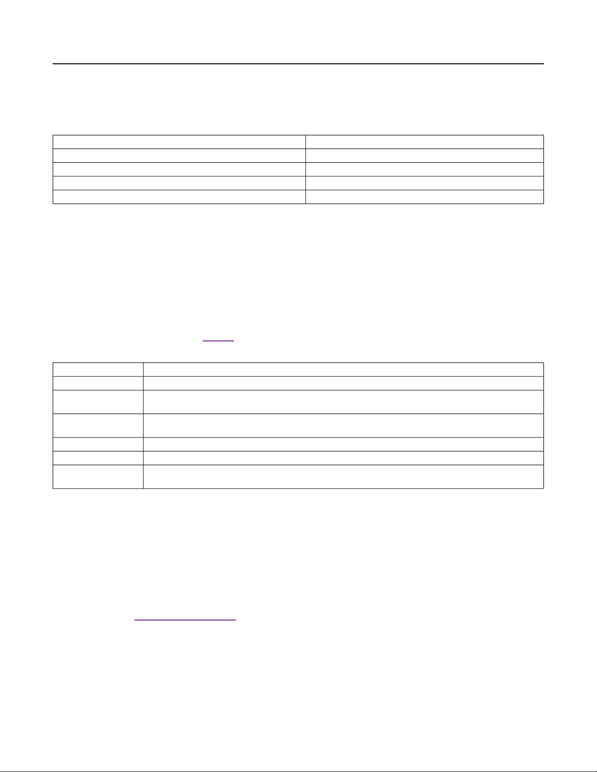
MAX78000 Ultra-Low-Power Arm Cortex-M4 Processor with
FPU-Based Microcontroller with Convolutional
Neural Network Accelerator
Table 1. BACKUP Mode SRAM Retention
RAM BLOCK RAM SIZE
SRAM0 32KB + ECC
SRAM1 32KB
SRAM2 48KB
SRAM3 16KB
POWER DOWN Mode (PDM)
This mode is used during product level distribution and storage. The device status is as follows:
● CM4 and RV32 are powered off.
● All peripherals and SRAM are powered down.
● All oscillators are powered down.
● There is no data retention in this mode, but values in flash memory are preserved.
● Voltage monitors are operational.
Wakeup Sources
The sources of wakeup from the SLEEP, LOW POWER, MICRO POWER, STANDBY, BACKUP, and POWER DOWN
operating modes are summarized in Table 2.
Table 2. Wakeup Sources
OPERATING MODE WAKEUP SOURCE
SLEEP Any enabled peripheral with interrupt capability; RSTN
LOW POWER (LPM)
MICRO POWER
(μPM)
STANDBY RTC, wakeup timer, GPIOs, CMP0, RSTN
BACKUP RTC, wakeup timer, GPIOs, CMP0, RSTN
POWER DOWN
(PDM)
SPI0, I2S, I2C, UARTs, timers, watchdog timers, wakeup timer, all comparators, RTC, GPIOs, RSTN, and
RV32
All comparators, LPUART, LPTMR1, LPTIMER2, LPWDT0, RTC, wakeup timer, GPIOs, RSTN
P3.0, P3.1, RSTN
Real-Time Clock
An RTC keeps the time of day in absolute seconds. The 32-bit seconds register can count up to approximately 136 years
and be translated to calendar format by application software.
The RTC provides a time-of-day alarm that can be programmed to any future value between 1 second and 12 days.
When configured for long intervals, the time-of-day alarm can be used as a power-saving timer, allowing the device to
remain in an extremely low-power mode, but still awaken periodically to perform assigned tasks. A second independent
32-bit 1/4096 subsecond alarm can be programmed with a tick resolution of 244μs. Both can be configured as recurring
alarms. When enabled, either alarm can cause an interrupt or wake the device from most low-power modes.
The time base is generated by a 32.768kHz crystal or an external clock source that must meet the electrical/timing
requirements in the Electrical Characteristics table.
The RTC calibration feature provides the ability for user software to compensate for minor variations in the RTC oscillator,
crystal, temperature, and board layout. Enabling the SQWOUT alternate function outputs a timing signal derived from the
RTC. External hardware can measure the frequency and adjust the RTC frequency in increments of ±127ppm with 1ppm
resolution. Under most circumstances, the oscillator does not require any calibration.
Programmable Timers
www.maximintegrated.com
19-100868
Maxim Integrated | 39
Page 40

MAX78000 Ultra-Low-Power Arm Cortex-M4 Processor with
FPU-Based Microcontroller with Convolutional
Neural Network Accelerator
32-Bit Timer/Counter/PWM (TMR, LPTMR)
General-purpose, 32-bit timers provide timing, capture/compare, or generation of pulse-width modulated (PWM) signals
with minimal software interaction.
The timer provides the following features:
● 32-bit up/down autoreload
● Programmable prescaler
● PWM output generation
● Capture, compare, and capture/compare capability
● External pin multiplexed with GPIO for timer input, clock gating, or capture
● Timer output pin
● TMR0–TMR3 can be configured as 2 × 16-bit general-purpose timers
● Timer interrupt
The MAX78000 provides six 32-bit timers (TMR0, TMR1, TMR2, TMR3, LPTMR0, and LPTMR1). LPTMR0 and LPTMR1
are capable of operation in the SLEEP, LOW POWER, and MICRO POWER modes.
I/O functionality is supported for all of the timers. Note that the function of a port can be multiplexed with other functions
on the GPIO pins, so it might not be possible to use all of the ports depending on the device configuration. See Table 3
for individual timer features.
Table 3. Timer Configuration Options
REGISTER
INSTANCE
TMR0 TMR0 Yes Yes No
TMR1 TMR1 Yes Yes No
TMR2 TMR2 Yes Yes No
TMR3 TMR3 Yes Yes No
LPTMR0 TMR4 No No Yes
LPTMR1 TMR5 No No Yes
ACCESS
NAME
SINGLE
32 BIT
DUAL
16
BIT
SINGLE
16 BIT
POWER
MODE
ACTIVE,
SLEEP,
LOW
POWER
ACTIVE,
SLEEP,
LOW
POWER
ACTIVE,
SLEEP,
LOW
POWER
ACTIVE,
SLEEP,
LOW
POWER
ACTIVE,
SLEEP,
LOW
POWER,
MICRO
POWER
ACTIVE,
SLEEP,
LOW
POWER,
MICRO
POWER
CLOCK SOURCE
PCLK ISO IBRO INRO ERTCO LPTMR0_CLK LPTMR1_CLK
Yes Yes Yes No Yes No No
Yes Yes Yes No Yes No No
Yes Yes Yes No Yes No No
Yes Yes Yes No Yes No No
No No Yes Yes Yes Yes No
No No Yes Yes Yes No Yes
www.maximintegrated.com
19-100868
Maxim Integrated | 40
Page 41
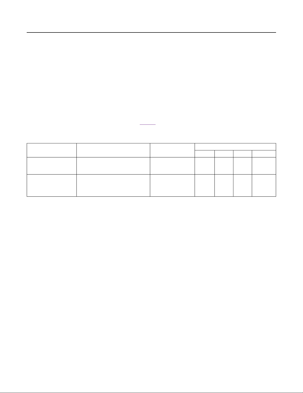
MAX78000 Ultra-Low-Power Arm Cortex-M4 Processor with
FPU-Based Microcontroller with Convolutional
Neural Network Accelerator
Watchdog Timer (WDT)
Microcontrollers are often used in harsh environments where electrical noise and electromagnetic interference (EMI) are
abundant. Without proper safeguards, these hazards can disturb device operation and corrupt program execution. One
of the most effective countermeasures is the windowed watchdog timer (WDT), which detects runaway code or system
unresponsiveness.
The WDT is a 32-bit, free-running counter with a configurable prescaler. When enabled, the WDT must be periodically
reset by the application software. Failure to reset the WDT within the user-configurable timeout period indicates that the
application software is not operating correctly and results in a WDT timeout. A WDT timeout can trigger an interrupt,
system reset, or both. Either response forces the instruction pointer to a known good location before resuming instruction
execution. The windowed timeout period feature provides more detailed monitoring of system operation, requiring the
WDT to be reset within a specific window of time. See Table 4 for individual timer features.
The MAX78000 provides two instances of the watchdog timer—WDT0 and LPWDT0.
Table 4. Watchdog Timer Configuration Options
INSTANCE NAME REGISTER ACCESS NAME POWER MODE
ACTIVE,
WDT0 WDT0
LPWDT0 WDT1
SLEEP,
LOW POWER
ACTIVE,
SLEEP,
LOW POWER,
MICRO POWER
PCLK IBRO INRO ERTCO
Yes Yes No No
No Yes Yes Yes
CLOCK SOURCE
Pulse Train Engine (PT)
Multiple, independent pulse train generators can provide either a square-wave or a repeating pattern from 2 to 32 bits
in length. Any single pulse train generator or any desired group of pulse train generators can be synchronized at the bit
level, allowing for multibit patterns. Each pulse train generator is independently configurable.
The pulse train generators provide the following features:
● Independently enabled
● Safe enable and disable for pulse trains without bit banding
● Multiple pin configurations allow for flexible layout
● Pulse trains can be started/synchronized independently or as a group
● Frequency of each enabled pulse train generator is also set separately, based on a divide down (such as divide by 2,
divide by 4, and divide by 8) of the input pulse train module clock
● Input pulse train module clock can be optionally configured to be independent from the system AHB clock
● Multiple repetition options
• Single shot (nonrepeating pattern of 2 to 32 bits)
• Pattern repeats user-configurable number of times or indefinitely
• Termination of one pulse train loop count can restart one or more other pulse trains
The pulse train engine feature is an alternate function associated with a GPIO pin. In most cases, enabling the pulse train
engine function supersedes the GPIO function.
The MAX78000 provide up to four instances of the pulse train engine peripheral (PT[3:0]).
Serial Peripherals
I2C Interface (I2C)
The I2C interface is a bidirectional, two-wire serial bus that provides a medium-speed communications network. It can
operate as a one-to-one, one-to-many or many-to-many communications medium. These engines support standard-
www.maximintegrated.com
19-100868
Maxim Integrated | 41
Page 42

MAX78000 Ultra-Low-Power Arm Cortex-M4 Processor with
FPU-Based Microcontroller with Convolutional
Neural Network Accelerator
mode, fast-mode, fast-mode plus and high-speed mode I2C speeds. It provides the following features:
● Master or slave mode operation
• Supports up to 4 different slave addresses in slave mode
● Supports standard 7-bit addressing or 10-bit addressing
● RESTART condition
● Interactive receive mode
● Tx FIFO preloading
● Support for clock stretching to allow slower slave devices to operate on higher speed busses
● Multiple transfer rates
• Standard mode: 100kbps
• Fast mode: 400kbps
• Fast mode plus: 1000kbps
• High-speed mode: 3.4Mbps
● Internal filter to reject noise spikes
● Receiver FIFO depth of 8 bytes
● Transmitter FIFO depth of 8 bytes
The MAX78000 provides three instances of the I2C peripheral—I2C0, I2C1, and I2C2.
I2S Interface (I2S)
The I2S interface is a bidirectional, four-wire serial bus that provides serial communications for codecs and audio
amplifiers compliant with the I2S Bus Specification, June 5, 1996. It provides the following features:
● Master and slave mode operation
● Support for 4 channels
● 8, 16, 24, and 32 bit frames
● Receive and transmit DMA support
● Wakeup on FIFO status (full/empty/threshold)
● Pulse density modulation support for receive channel
● Word select polarity control
● First bit position selection
● Interrupts generated for FIFO status
● Receiver FIFO depth of 32 bytes
● Transmitter FIFO depth of 32 bytes
The MAX78000 provides one instance of the I2S peripheral (I2S0).
Serial Peripheral Interface (SPI)
SPI is a highly configurable, flexible, and efficient synchronous interface among multiple SPI devices on a single bus. The
bus uses a single clock signal and multiple data signals, and one or more slave select lines to address only the intended
target device. The SPI operates independently and requires minimal processor overhead.
The provided SPI peripherals can operate in either slave or master mode and provide the following features:
● SPI modes 0, 1, 2, or 3 for single-bit communication
● 3- or 4-wire mode for single-bit slave device communication
● Full-duplex operation in single-bit, 4-wire mode
● Dual and quad data modes supported
● Multiple slave selects on some instances
● Multimaster mode fault detection
● Programmable interface timing
● Programmable SCK frequency and duty cycle
● 32-byte transmit and receive FIFOs
● Slave select assertion and deassertion timing with respect to leading/trailing SCK edge
www.maximintegrated.com
19-100868
Maxim Integrated | 42
Page 43
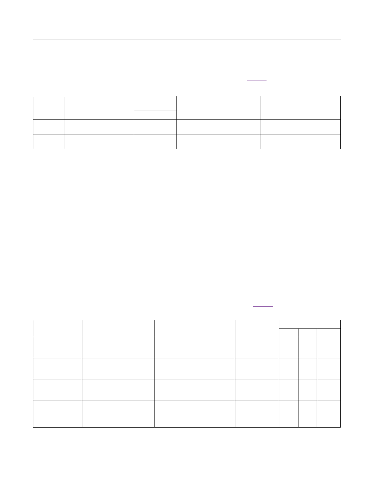
MAX78000 Ultra-Low-Power Arm Cortex-M4 Processor with
FPU-Based Microcontroller with Convolutional
Neural Network Accelerator
The MAX78000 provides two instances of the SPI peripheral—SPI0 and SPI1. See Table 5 for configuration options.
Table 5. SPI Configuration Options
SLAVE
INSTANCE DATA
SPI0
SPI1
3-wire, 4-wire, dual, or
quad data support
3-wire, 4-wire, dual, or
quad data support
SELECT LINES
81 CTBGA
3 50 50
1 25 50
UART (UART, LPUART)
The universal asynchronous receiver-transmitter (UART, LPUART) interface supports full-duplex asynchronous
communication with optional hardware flow control (HFC) modes to prevent data overruns. If HFC mode is enabled on a
given port, the system uses two extra pins to implement the industry-standard request to send (RTS) and clear to send
(CTS) flow control signaling. Each instance is individually programmable.
● 2-wire interface or 4-wire interface with flow control
● 8-byte send/receive FIFO
● Full-duplex operation for asynchronous data transfers
● Interrupts available for frame error, parity error, CTS, Rx FIFO overrun, and FIFO full/partially full conditions
● Automatic parity and frame error detection
● Independent baud-rate generator
● Programmable 9th-bit parity support
● Multidrop support
● Start/stop bit support
● Hardware flow control using RTS/CTS
● 12.5Mbps for UART maximum bit rate
● 1.85Mbps for LPUART maximum bit rate
● Two DMA channels can be connected (read and write FIFOs)
● Programmable word size (5 bits to 8 bits)
The MAX78000 provides four instances of the UART peripheral—UART0, UART1, UART2, and LPUART0. LPUART0 is
capable of operation in the SLEEP, LOW POWER, and MICRO POWER modes. See Table 6 for configuration options.
MAXIMUM FREQUENCY
MASTER MODE (MHz)
MAXIMUM FREQUENCY
SLAVE MODE (MHz)
Table 6. UART Configuration Options
INSTANCE NAME REGISTER ACCESS NAME HARDWARE FLOW CONTROL POWER MODE
ACTIVE,
UART0 UART0 Yes
UART1 UART1 No
UART2 UART2 No
LPUART0 UART3 No
www.maximintegrated.com
19-100868
SLEEP,
LOW POWER
ACTIVE,
SLEEP,
LOW POWER
ACTIVE,
SLEEP,
LOW POWER
ACTIVE,
SLEEP,
LOW POWER,
MICRO POWER
CLOCK SOURCE
PCLK IBRO ERTCO
Yes Yes No
Yes Yes No
Yes Yes No
No Yes Yes
Maxim Integrated | 43
Page 44

MAX78000 Ultra-Low-Power Arm Cortex-M4 Processor with
FPU-Based Microcontroller with Convolutional
Neural Network Accelerator
1-Wire Master (OWM)
Maxim's 1-Wire bus consists of one signal that carries data and also supplies power to the slave devices and a ground
return. The bus master communicates serially with one or more slave devices through the bidirectional, multidrop 1-Wire
bus. The single-contact serial interface is ideal for communication networks requiring minimal interconnection.
The provided 1-Wire master supports the following features:
● Single contact for control and operation
● Unique factory identifier for any 1-Wire device
● Multiple device capability on a single line
The OWM supports both standard (15.6kbps) and overdrive (110kbps) speeds.
Standard DMA Controller
The standard DMA controller allows automatic one-way data transfer between two entities. These entities can be
either memories or peripherals. The transfers are done without using CPU resources. The following transfer modes are
supported:
● 4-channel
● Peripheral to data memory
● Data memory to peripheral
● Data memory to data memory
● Event support
All DMA transactions consist of an AHB burst read into the DMA FIFO followed immediately by an AHB burst write from
the FIFO.
The MAX78000 provides one instance of the standard DMA controller.
Security
AES
The dedicated hardware-based AES engine supports the following algorithms:
● AES-128
● AES-192
● AES-256
The AES keys are automatically generated by the engine and stored in dedicated flash to protect against tampering. Key
generation and storage is transparent to the user.
True Random Number Generator (TRNG) Non-Deterministic Random Bit Generator (NDRBG)
The device provides a non-deterministic entropy source that can be used to generate cryptographic seeds or strong
encryption keys as part of an overall framework for a secure customer application.
Software can use random numbers to trigger asynchronous events that add complexity to program execution to thwart
replay attacks or key search methodologies.
The TRNG can support the system-level validation of many security standards. Maxim Integrated will work directly with
the customer’s validation laboratory to provide the laboratory with any required information. Contact Maxim Integrated for
details of compliance with specific standards.
CRC Module
A cyclic redundancy check (CRC) hardware module provides fast calculations and data integrity checks by application
software. It supports a user-defined programmable polynomial up to 32-bits. Direct memory access copies data into
the CRC module so that CRC calculations on large blocks of memory are performed with minimal CPU intervention.
Examples of common polynomials are depicted in Table 7.
www.maximintegrated.com
19-100868
Maxim Integrated | 44
Page 45
MAX78000 Ultra-Low-Power Arm Cortex-M4 Processor with
FPU-Based Microcontroller with Convolutional
Neural Network Accelerator
Table 7. Common CRC Polynomials
ALGORITHM POLYNOMIAL EXPRESSION ORDER POLYNOMIAL CHECK
CRC-32-ETHERNET
CRC-CCITT x16+ x12+ x5+ x
CRC-16 x16+ x15+ x2+ x
USB DATA x16+ x15+ x2+ x
PARITY x1+ x
x32+ x26+ x23+ x22+ x16+ x12+ x11+ x10+ x8+ x7+ x5+ x4+
x2+ x1+ x
0
0
0
0
0
Bootloader
The bootloader allows loading and verification of program memory through a UART or SWD interface. It provides the
following features:
● Program loading of Motorola®SREC format files
● Permanent lock state prevents altering or erasing program memory
● Access to the USN for device or customer application identification
● Disable SWD interface to block debug access port functionality
0xEDB8
8320
0x0000
8408
0x0000
A001
0x8005
0000
0x0000
0001
LSB
LSB
LSB
LSB
MSB —
0xDEBB
20E3
0x0000
F0B8
0x0000
B001
0x800D
0000
Secure Bootloader
Versions of the device which support the secure feature provides the following features:
● Optional challenge/response through secret HMAC SHA-256 authenticates host before executing bootloader
commands
● Automatic program memory verification and authentication before execution after every reset (secure boot)
Debug and Development Interface (SWD, JTAG)
The serial wire debug interface is used for code loading and ICE debug activities for the CM4. JTAG interface is provided
for the RV32. All devices in mass production have the debugging/development interface enabled.
Motorola is a registered trademark and registered service mark of Motorola Trademark Holdings, LLC.
www.maximintegrated.com
19-100868
Maxim Integrated | 45
Page 46

MAX78000 Ultra-Low-Power Arm Cortex-M4 Processor with
FPU-Based Microcontroller with Convolutional
Neural Network Accelerator
Applications Information
Bypass Capacitors
The proper use of bypass capacitors reduces noise generated by the IC into the ground plane. The Pin Descriptions table
indicates which pins should be connected to bypass capacitors, and the appropriate ground plane.
It is recommended that one instance of a bypass capacitor should be connected to each pin/ball of the IC package. For
example, if the Pin Descriptions table shows 4 device pins associated with voltage supply A, a separate capacitor should
be connected to each pin for a total of 4 capacitors.
Capacitors should be placed as close as possible to their corresponding device pins. Pin descriptions which indicate
recommendations for more than one value of capacitor per pin should place them in parallel with the lowest value
capacitor first, closest to the pin.
Ordering Information
PART
MAX78000EXG+ 512 128 +
FLASH
(KB)
SYSTEM
RAM
(KB)
ECC 8
BOOTLOADER
Yes No 81 CTBGA
SECURE
BOOTLOADER
PIN-PACKAGE
www.maximintegrated.com
19-100868
Maxim Integrated | 46
Page 47
MAX78000 Ultra-Low-Power Arm Cortex-M4 Processor with
FPU-Based Microcontroller with Convolutional
Neural Network Accelerator
Revision History
REVISION
NUMBER
0 08/20 Release for intro —
REVISION
DATE
DESCRIPTION
PAGES
CHANGED
For pricing, delivery, and ordering information, please visit Maxim Integrated’s online storefront at https://www.maximintegrated.com/en/storefront/storefront.html.
Maxim Integrated cannot assume responsibility for use of any circuitry other than circuitry entirely embodied in a Maxim Integrated product. No circuit patent
licenses are implied. Maxim Integrated reserves the right to change the circuitry and specifications without notice at any time. The parametric values (min and max
limits) shown in the Electrical Characteristics table are guaranteed. Other parametric values quoted in this data sheet are provided for guidance.
Maxim Integrated and the Maxim Integrated logo are trademarks of Maxim Integrated Products, Inc. © 2020 Maxim Integrated Products, Inc.
 Loading...