

Datasheet MAX4403AUD, MAX4403ASD, MAX4402ASA, MAX4402AKA-T, MAX4400AXK-T Datasheet (Maxim)
...Page 1
General Description
The MAX4400–MAX4403 low-cost, general-purpose op
amps offer Rail-to-Rail®outputs, draw only 320µA of quiescent current, and operate from a single +2.5V to +5.5V
supply. For additional power conservation, the MAX4401
offers a low-power shutdown mode that reduces supply
current to 1µA max and puts the amplifier’s outputs in a
high-impedance state. These devices deliver ±1.4mA of
output current and are unity-gain stable with a 1MHz gainbandwidth product driving capacitive loads up to 400pF.
The MAX4400–MAX4403 are specified to +125°C, making
them suitable for use in a variety of harsh environments,
such as automotive applications.
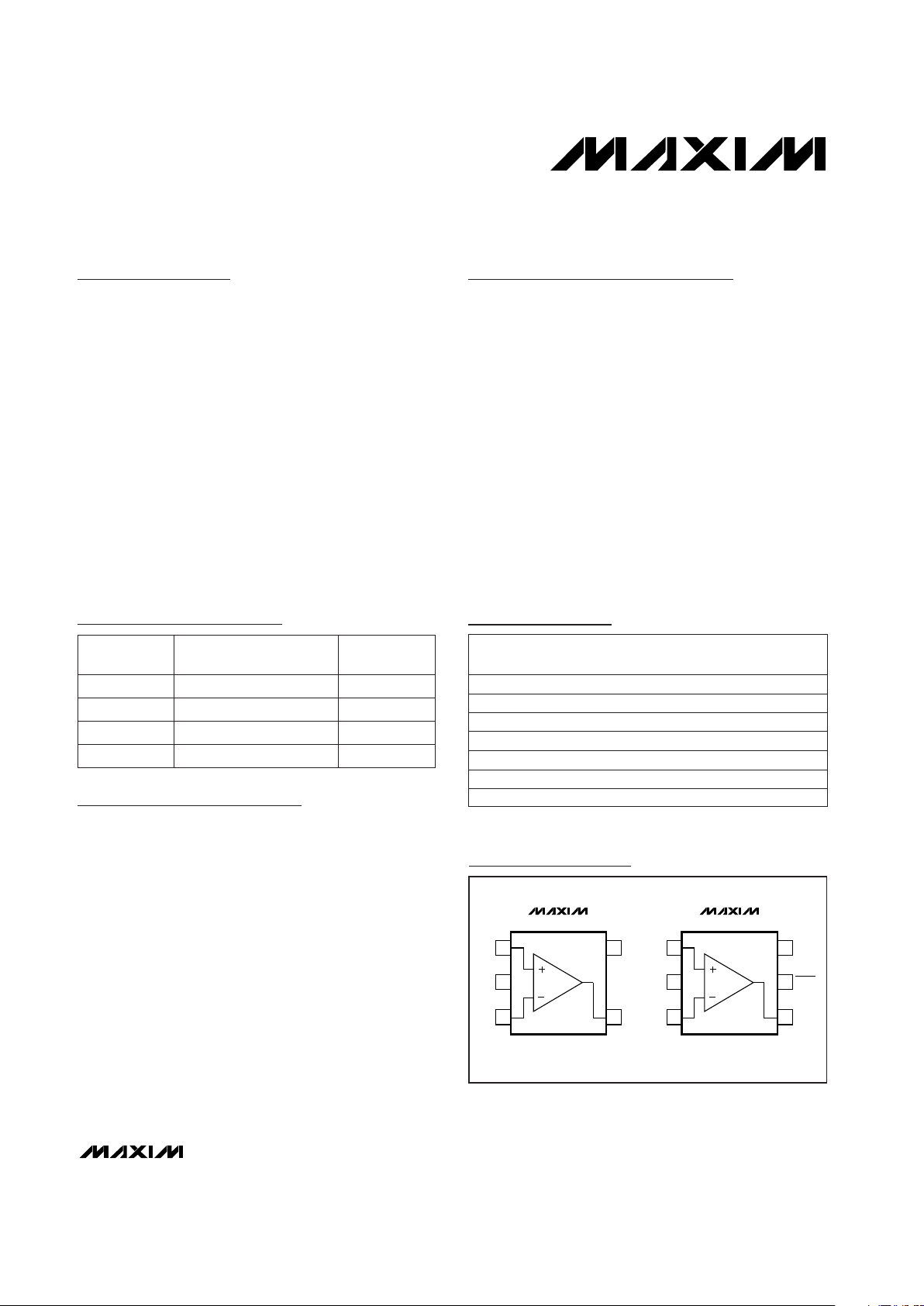
The MAX4400 single amplifier is available in ultra-small
5-pin SC70 and space-saving 5-pin SOT23 packages.
The single MAX4401 includes the shutdown feature and is
available in a 6-pin SC70. The MAX4402 is a dual amplifier
available in 8-pin SOT23 and SO packages. The
MAX4403 quad amplifier comes packaged in a 14-pin
TSSOP or SO.
Applications
Single-Supply Zero-Crossing Detectors
Instruments and Terminals
Portable Communications
Electronic Ignition Modules
Infrared Receivers
Sensor Signal Detection
Features
♦ Single +2.5V to +5.5V Supply Voltage Range
♦ 320µA Quiescent Current per Amplifier
♦ 1µA max Shutdown Mode (MAX4401)
♦ Available in Space-Saving Packages
5-Pin SC70 (MAX4400)
6-Pin SC70 (MAX4401)
8-Pin SOT23 (MAX4402)
♦ 110dB A
VOL
with 2kΩ Load
♦ 0.015% THD with 2kΩ Load
♦ Rail-to-Rail Output Voltage Swing
♦ 1.4mA of Sink and Source Load Current
♦ Unity-Gain Stable up to C
LOAD
= 400pF
♦ Ground-Sensing Inputs
For free samples and the latest literature, visit www.maxim-ic.com or phone 1-800-998-8800.
For small orders, phone 1-800-835-8769.
MAX4400–MAX4403
Single/Dual/Quad, Low-Cost, Single-Supply,
Rail-to-Rail Op Amps with Shutdown
________________________________________________________________ Maxim Integrated Products 1
IN+
IN-
1
2
3
5
4
OUT
V
SS
VDDIN+
IN-
1
2
3
6
5
4
OUT
SHDN
V
SS
V
DD
MAX4400 MAX4401
SC70-5/SOT23-5 SC70-6
19-1599; Rev 0; 1/00
PART
MAX4400AXK-T
MAX4400AUK-T
MAX4401AXT-T
-40°C to +125°C
-40°C to +125°C
-40°C to +125°C
TEMP. RANGE
PIN-
PACKAGE
5 SC70-5
5 SOT23-5
6 SC70-6
*Future product—contact factory for availability.
Pin Configurations
Ordering Information
Selector Guide
MAX4402AKA-T*
MAX4402ASA*
MAX4403AUD*
-40°C to +125°C
-40°C to +125°C
-40°C to +125°C 8 SOT23-8
8 SO
14 TSSOP
MAX4403ASD* -40°C to +125°C 14 SO
MAX4401 1 Yes
MAX4402 2 No
MAX4403 4 No
Rail-to-Rail is a registered trademark of Nippon Motorola, Ltd.
Pin Configurations continued at end of data sheet.
No1MAX4400
PART
NO. OF AMPLIFIERS
PER PACKAGE
SHUTDOWN
MODE
TOP
MARK
AAG
ADNP
AAB
AADI
—
—
—
Page 2
MAX4400–MAX4403
Single/Dual/Quad, Low-Cost, Single-Supply,
Rail-to-Rail Op Amps with Shutdown
2 _______________________________________________________________________________________
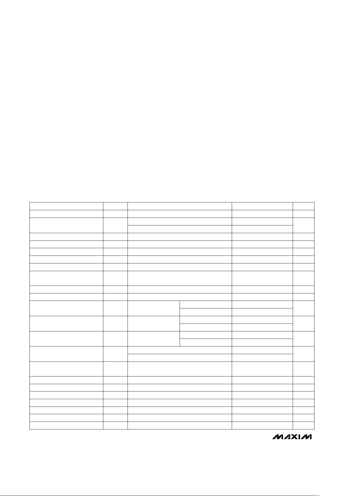
ABSOLUTE MAXIMUM RATINGS
ELECTRICAL CHARACTERISTICS
(VDD= +5V, VSS= 0, VCM= 0, V
OUT
= VDD/2, RL= ∞ connected to VDD/2, SHDN = VDD(MAX4401 only), TA= +25°C, unless
otherwise noted.)
Stresses beyond those listed under “Absolute Maximum Ratings” may cause permanent damage to the device. These are stress ratings only, and functional
operation of the device at these or any other conditions beyond those indicated in the operational sections of the specifications is not implied. Exposure to
absolute maximum rating conditions for extended periods may affect device reliability.
Power-Supply Voltage (VDDto VSS) .........................-0.3V to +6V
All Other Pins ...................................(VSS- 0.3V) to (VDD+ 0.3V)
Output Short-Circuit Duration
(OUT shorted to VSSor VDD)................................. Continuous
Continuous Power Dissipation (TA= +70°C)
5-Pin SC70 (derate 2.5mW/°C above +70°C)............. 200mW
6-Pin SC70 (derate 2.27mW/°C above +70°C)............181mW
5-Pin SOT23 (derate 7.1mW/°C above +70°C)............571mW
8-Pin SOT23 (derate 7.52mW/°C above +70°C)..........602mW
8-Pin SO (derate 5.88mW/°C above +70°C)............... 471mW
14-Pin TSSOP (derate 8.33mW/°C above +70°C) ...... 667mW
14-Pin SO (derate 8.33mW/°C above +70°C)............. 667mW
Operating Temperature Range .........................-40°C to +125°C
Storage Temperature Range .............................-65°C to +150°C
Lead Temperature (soldering, 10s) .................................+300°C
SHDN = VDDor VSS(Notes 1, 2)
(Note 1)
VDD= 5.0V
(Note 1)
Device in shutdown mode, SHDN = VSS,
V
SS
< V
OUT
< VCC(Note 1)
V
DD
= 2.5V
Sinking
Inferred from PSRR test
Sourcing
Specified as
|VSS- VOL|
2.5V ≤ VDD≤ 5.5V
VSS≤ VCM≤ VDD- 1.4V
Specified as
|V
DD
- VOH|
Inferred from CMRR test
Differential or common mode
SHDN = VSS(Note 1)
(Note 2)
dB
(Note 2)
VSS+ 0.3V ≤
V
OUT
≤ VDD- 0.3V
CONDITIONS
kHz
800
GBWGain-Bandwidth Product
pA
±1 ±100
IIL, I
IH
SHDN Input Current
V
0.7 · V
DD
V
IH
SHDN Logic High
V
0.3 · V
DD
V
IL
SHDN Logic Low
µA
±1.0
I
OUTSHDN
Shutdown Mode Output
Leakage
30
mA
12
Output Short-Circuit Current
30 75
mV
2
V
OL
Output Voltage Low
55 200
mV
3
V
OH
Output Voltage High
90 110
dB
120
A
VOL
Large-Signal Voltage Gain
400 700
RL= 100kΩ
RL= 2kΩ
µA
320
I
DD
V
2.5 5.5
V
DD
Supply Voltage Range
Supply Current per Amplifier
78 100
PSRRPower-Supply Rejection Ratio
dB
68 84
CMRRCommon-Mode Rejection Ratio
V
V
SS
VDD- 1.4
V
CM
Input Common-Mode Voltage
Range
GΩ
1000
R
IN
Input Resistance
µA
0.00002 1
I
SHDN
Supply Current in Shutdown
mV
±0.8 ±4.5
V
OS
Input Offset Voltage
pA
±0.1 ±100
I
B
Input Bias Current
pA
±0.1 ±100
I
OS
Input Offset Current
UNITSMIN TYP MAXSYMBOLPARAMETER
RL= 100kΩ
RL= 2kΩ
RL= 100kΩ
RL= 2kΩ
degrees
70
φ
M
Phase Margin
dB
20
Gain Margin
V/µs
1
SRSlew Rate
Page 3
MAX4400–MAX4403
Single/Dual/Quad, Low-Cost, Single-Supply,
Rail-to-Rail Op Amps with Shutdown
_______________________________________________________________________________________ 3
Total Harmonic Distortion
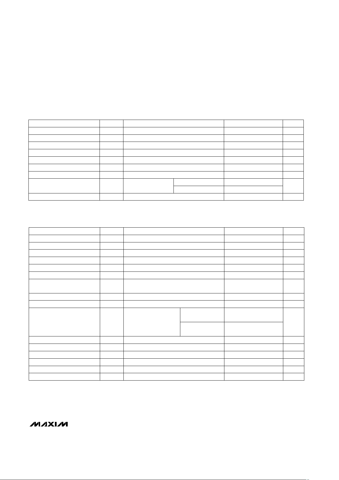
ELECTRICAL CHARACTERISTICS (continued)
(VDD= +5V, VSS= 0, VCM= 0, V
OUT
= VDD/2, RL= ∞ connected to VDD/2, SHDN = VDD(MAX4401 only), TA= +25°C, unless
otherwise noted.)
ELECTRICAL CHARACTERISTICS
(VDD= +5V, VSS= 0, VCM= 0, V
OUT
= VDD/2, RL= ∞ connected to VDD/2, TA= -40°C to +125°C, unless otherwise noted.) (Note 3)
Note 1: Shutdown mode is only available in the 6-pin SC70 single op amp (MAX4401).
Note 2: Guaranteed by design.
Note 3: Specifications are 100% tested at T
A
= +25°C (exceptions noted). All temperature limits are guaranteed by design.
RL= 100kΩ
RL= 2kΩ
CONDITIONS UNITSMIN TYP MAXSYMBOLPARAMETER
V
OUT
= 2V step
(Note 1)
AV= 1V/V
f = 10kHz, V
OUT
=
2Vp-p, AV= 1V/V
f = 10kHz
f = 10kHz
(Note 1)
µs
7
t
S
Settling Time to 0.1%
0.015
%
0.009
THDTotal Harmonic Distortion
pF
2.5
C
IN
Input Capacitance
µs
5
t
ON
Power-On Time
µs
6
t
EN
Enable Delay Time
µs
0.4
t
SHDN
Shutdown Delay Time
pF
400
C
LOAD
Capacitive-Load Stability
fA/√Hz
1
i
n
Input Current Noise Density
nV/√Hz
36e
n
Input Voltage Noise Density
+85°C to +125°C
-40°C to +85°C
±5.0
Device in shutdown
mode, SHDN = V
SS
,
V
SS
< V
OUT
< V
DD
(Note 1)
Inferred from PSRR test
Specified as |VSS- VOL|, RL = 2kΩ
Specified as |VDD- VOH|, RL= 2kΩ
VSS+ 0.3V ≤ V
OUT
≤ VDD- 0.3V, RL= 2kΩ
SHDN = VDDor VSS(Notes 1, 2)
(Note 1)
2.5V ≤ VCC≤ 5.5V
V
SS
≤ VCM≤ VDD- 1.5V
(Note 2)
(Note 2)
(Note 1)
Inferred from CMRR test
CONDITIONS
mV
100
V
OL
Output Voltage Low
mV
250
V
OH
Output Voltage High
dB
85
A
VOL
Large-Signal Voltage Gain
pA
±100
I
IL,IIH
SHDN Input Current
V
0.7 · V
DD
V
IH
SHDN Logic High
V
0.3 · V
DD
V
IL
SHDN Logic Low
mV
±6.5
V
OS
Input Offset Voltage
µA
800
I
DD
V
2.5 5.5
V
DD
Supply Voltage Range
Supply Current per Amplifier
µA
±1.0
I
OUTSHDN
Shutdown Mode Output
Leakage
dB
74
PSRRPower-Supply Rejection Ratio
dB
65
CMRRCommon-Mode Rejection Ratio
µV/°C
±1
TC
VOS
Input Offset Voltage Drift
pA
±100
I
B
Input Bias Current
pA
±100
I
OS
Input Offset Current
V
V
SS
V
DD
- 1.5
V
CM
Input Common-Mode Voltage
Range
UNITSMIN TYP MAXSYMBOLPARAMETER
Page 4
MAX4400–MAX4403
Single/Dual/Quad, Low-Cost, Single-Supply,
Rail-to-Rail Op Amps with Shutdown
4 _______________________________________________________________________________________
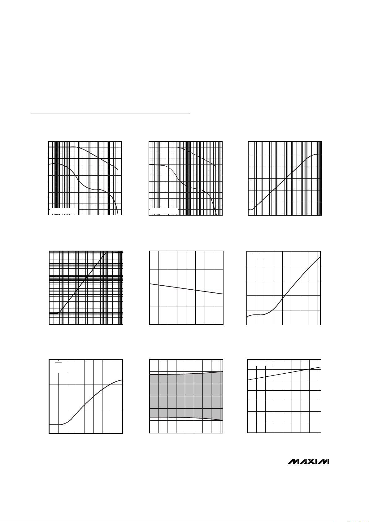
Typical Operating Characteristics
(VDD= +5V, VSS= 0, VCM= VDD/2, V
SHDN
= 5V, RL= ∞ connected to VDD/2, TA= +25°C, unless otherwise noted.)
80
60
40
20
0
-20
-40
-60
-80
-100
-120
-140
-160
-180
1 10 1k 10M1M
GAIN AND PHASE
vs. FREQUENCY (NO LOAD)
MAX4400 toc01
FREQUENCY (Hz)
GAIN (dB)/PHASE (deg)
100 10k 100k
A
VCL
= +1000V/V
80
60
40
20
0
-20
-40
-60
-80
-100
-120
-140
-160
-180
1 10 1k 10M1M
GAIN AND PHASE vs. FREQUENCY
(C
L
= 400pF)
MAX4400 toc02
FREQUENCY (Hz)
GAIN (dB)/PHASE (deg)
100 10k 100k
A
VCL
= +1000V/V
10 1k100 10k 100k 1M
POWER-SUPPLY REJECTION RATIO
vs. FREQUENCY
MAX4400 toc03
FREQUENCY (Hz)
PSRR (dB)
10
-110
-90
-10
-30
-50
-70
FREQUENCY (Hz)
1000
0.001
10 100 1k 10k 100k 1M
OUTPUT IMPEDANCE
vs. FREQUENCY
0.1
MAX4400 toc4
OUTPUT IMPEDANCE (Ω)
10
0.01
1
100
300
350
400
450
500
-40 0 40 80-20 20 60 100 120
SUPPLY CURRENT vs. TEMPERATURE
MAX4400 toc05
TEMPERATURE (°C)
SUPPLY CURRENT (µA)
1
10
100
1k
10k
1M
-40 0 40 80-20 20 60 100 120
MAX4401
SHUTDOWN SUPPLY CURRENT
vs. TEMPERATURE
MAX4400 toc06
TEMPERATURE (°C)
SUPPLY CURRENT (pA)
V
SHDN
= V
SS
0.1
10
1k
1M
-40 0 40 80-20 20 60 100 120
MAX4401
OUTPUT LEAKAGE CURRENT
vs. TEMPERATURE
MAX4400 toc07
TEMPERATURE (°C)
I
LEAK
(pA)
V
SHDN
= V
SS
V
OUT = VDD/2
-1500
-1000
-500
500
0
1000
1500
-40 0 40 80-20 20 60 100 120
INPUT OFFSET VOLTAGE
vs. TEMPERATURE
MAX4400 toc08
TEMPERATURE (°C)
V
OS
(µV)
30
20
10
0
50
40
70
60
-40 0 40 80-20 20 60 100 120
OUTPUT VOLTAGE SWING HIGH
vs. TEMPERATURE
MAX4400 toc09
TEMPERATURE (°C)
V
DD
-V
OH
(mV)
RL = 2kΩ to VDD/2
Page 5

MAX4400–MAX4403
Single/Dual/Quad, Low-Cost, Single-Supply,
Rail-to-Rail Op Amps with Shutdown
_______________________________________________________________________________________ 5
Typical Operating Characteristics (continued)
(VDD= +5V, VSS= 0, VCM= VDD/2, V
SHDN
= 5V, RL= ∞ connected to VDD/2, TA= +25°C, unless otherwise noted.)
0
10
20
30
40
50
-40 0 40 80-20 20 60 100 120
OUTPUT VOLTAGE SWING LOW
vs. TEMPERATURE
MAX4400 toc10
TEMPERATURE (°C)
V
OL
- V
EE
(mV)
RL = 2kΩ to VDD/2
-100
-90
-80
-70
-60
-40 0 40 80-20 20 60 100 120
COMMON-MODE REJECTION RATIO
vs. TEMPERATURE
MAX4400 toc11
TEMPERATURE (°C)
CMRR (dB)
0
40
80
60
20
100
120
140
0.5 1.5 2.5 3.51.0 2.0 3.0 4.0 4.5
LARGE-SIGNAL GAIN
vs. OUTPUT VOLTAGE
MAX4400 toc12
V
OUT
(V)
GAIN (dB)
RL = 2kΩ
100
115
110
105
120
130
125
140
135
-40 0 40 80-20 20 60 100 120
LARGE-SIGNAL GAIN
vs. TEMPERATURE
MAX4400 toc13
TEMPERATURE (°C)
GAIN (dB)
RL = 2kΩ
1.0
1.5
2.0
2.5
3.0
-40 0 40 80-20 20 60 100 120
MINIMUM OPERATING VOLTAGE
vs. TEMPERATURE
MAX4400 toc14
TEMPERATURE (°C)
V
MIN
(V)
10 1k100 10k 100k
TOTAL HARMONIC DISTORTION
vs. FREQUENCY
MAX4400 toc15
FREQUENCY (Hz)
THD (%)
0.1
0.01
0.0001
0.001
RL = 2kΩ
V
OUT
= 2Vp-p
A
V
= +1
10 1k100 10k 100k
TOTAL HARMONIC DISTORTION
vs. FREQUENCY
MAX4400 toc16
FREQUENCY (Hz)
THD (%)
0.01
0.0001
0.001
RL = 100kΩ
V
OUT
= 2Vp-p
A
V
= +1
0.0001
0.001
0.1
0.01
1
10
0 1.00.5 1.5 2.0 2.5 3.0
TOTAL HARMONIC DISTORTION
PLUS NOISE vs. INPUT AMPLITUDE
MAX4400 toc17
VIN (Vp-p)
THD + N (%)
RL = 2kΩ
f = 10kHz
BW = 20kHz
0.0001
0.001
0.1
0.01
1
10
0 1.00.5 1.5 2.0 2.5 3.0
TOTAL HARMONIC DISTORTION
PLUS NOISE vs. INPUT AMPLITUDE
MAX4400 toc18
VIN (Vp-p)
THD + N (%)
RL = 100kΩ
f = 10kHz
BW = 20kHz
Page 6

MAX4400–MAX4403
Single/Dual/Quad, Low-Cost, Single-Supply,
Rail-to-Rail Op Amps with Shutdown
6 _______________________________________________________________________________________
Typical Operating Characteristics (continued)
(VDD= +5V, VSS= 0, VCM= VDD/2, V
SHDN
= 5V, RL= ∞ connected to VDD/2, TA= +25°C, unless otherwise noted.)
CAPACITIVE-LOAD STABILITY
2000
0
1k 10k 100k
500
MAX4400 toc19
RESISTIVE LOAD (Ω)
CAPACITIVE LOAD (pF)
1000
1500
AV = +1
T
A
= +25°C
UNSTABLE
REGION
STABLE
REGION
2µs/div
IN
50mV/div
OUT
NONINVERTING SMALL-SIGNAL
TRANSIENT RESPONSE
MAX4400 toc20
AV = +1V/V
R
L
= 2kΩ
10µs/div
IN
2V/div
OUT
NONINVERTING LARGE-SIGNAL
TRANSIENT RESPONSE
MAX4400 toc21
AV = +1V/V
R
L
= 2kΩ
0
10
5
20
15
25
30
0 200 300100 400 500 600
PERCENT OVERSHOOT
vs. CAPACITIVE LOAD
MAX4400 toc22
C
LOAD
(pF)
OVERSHOOT (%)
NEGATIVE OVERSHOOT
POSITIVE OVERSHOOT
0
100
50
250
200
150
400
350
300
450
021 3456
SUPPLY CURRENT vs. SUPPLY VOLTAGE
MAX4400 toc24
SUPPLY VOLTAGE (V)
SUPPLY CURRENT (µA)
V
OUT
= VDD/2
Page 7

MAX4400–MAX4403
Single/Dual/Quad, Low-Cost, Single-Supply,
Rail-to-Rail Op Amps with Shutdown
_______________________________________________________________________________________ 7
FUNCTION
— — Noninverting Amplifier Input A
— — Noninverting Amplifier Input B
— — Noninverting Amplifier Input C
— — Noninverting Amplifier Input D
— — Inverting Amplifier Input B
— — Inverting Amplifier Input A
3 3 Inverting Amplifier Input
2 2
Negative Supply. Connect to ground for singlesupply operation
— — Amplifier Output B
— — Amplifier Output A
4 4 Amplifier Output
— — Inverting Amplifier Input D
— — Inverting Amplifier Input C
Pin Description
— 5
Active-Low Shutdown Input. Connect to VDDfor
normal operation. Do not leave floating.
5 6 Positive Supply
— — Amplifier Output D
— — Amplifier Output C
3
5
—
—
6
2
—
4
7
1
—
—
—
—
8
—
—
PIN
3
5
10
12
6
2
—
11
7
1
—
13
9
—
4
14
8
NAME
INA+
INB+
INC+
IND+
INB-
INA-
IN-
V
SS
OUTB
OUTA
OUT
IND-
INC-
SHDN
V
DD
OUTD
OUTC
1 Noninverting Amplifier Input1 — — IN+
MAX4401MAX4400 MAX4402 MAX4403
Detailed Description
Rail-to-Rail Output Stage
The MAX4400–MAX4403 can drive a 2kΩ load and still
typically swing within 55mV of the supply rails. Figure 1
shows the output voltage swing of the MAX4400 configured with AV = +10V/V.
Driving Capacitive Loads
Driving a capacitive load can cause instability in many
op amps, especially those with low quiescent current.
The MAX4400–MAX4403 are unity-gain stable for a
range of capacitive loads to above 400pF. Figure 2
shows the response of the MAX4400 with an excessive
capacitive load. Adding a series resistor between the
output and the load capacitor (Figure 3) improves the
1V/div
100µs/div
Figure 1. Rail-to-Rail Output Operation
Page 8

MAX4400–MAX4403
Single/Dual/Quad, Low-Cost, Single-Supply,
Rail-to-Rail Op Amps with Shutdown
8 _______________________________________________________________________________________
circuit’s response by isolating the load capacitance
from the op amp’s output.
Applications Information
Shutdown Mode
The MAX4401 features a low-power shutdown mode.
When SHDN goes low, the supply current drops to
0.1µA (typical). The output enters a high-impedance
state. Pull SHDN high to enable the amplifier. Do not
leave SHDN floating. Figure 4 shows the shutdown
waveform.
Power-Up
The MAX4400–MAX4403 outputs typically settle within
5µs after power-up. Figure 5 shows the output voltage
on power-up and power-down.
Power Supplies and Layout
The MAX4400–MAX4403 operate from a single +2.5V
to +5.5V power supply. Bypass the power supply with a
0.1µF capacitor to ground.
Good layout techniques optimize performance by
decreasing the amount of stray capacitance at the op
amp’s inputs and outputs. To decrease stray capacitance, minimize trace lengths by placing external components close to the op amp’s pins.
2µs/div
IN
50mV/div
OUT
R
ISO
C
L
MAX4400
MAX4401
MAX4402
MAX4403
Figure 3. Capacitive-Load-Driving Circuit
RL = 10MΩ TO GND
C
L
= 25pF
400µs/div
SHDN
2V/div
OUT
Figure 4. Shutdown Waveform
10µs/div
OUT
1V/div
V
DD
2V/div
Figure 5. Power-Up/Power-Down Waveform
Figure 2. Small-Signal Transient Response with Excessive
Capacitive Load
TRANSISTOR COUNT: 101 (MAX4400/MAX4401)
202 (MAX4402)
404 (MAX4403)
Chip Information
Page 9

MAX4400–MAX4403
Single/Dual/Quad, Low-Cost, Single-Supply,
Rail-to-Rail Op Amps with Shutdown
_______________________________________________________________________________________ 9
Package Information
SC70, 5L.EPS
6
SOT23-8/SO TSSOP/SO
V
SS
OUTA
INA+
1
2
3
4
8
INB-
5
INB+
7
OUTB
INA-
V
DD
OUTA
INA+
INB+
OUTB
INB-
1
2
3
4
5
6
7
14
13
12
11
10
9
8
IND+
INC+
INC-
OUTC
IND-
OUTD
INA-
V
DD
V
SS
MAX4403
MAX4402
Pin Configurations (continued)
Page 10

MAX4400–MAX4403
Single/Dual/Quad, Low-Cost, Single-Supply,
Rail-to-Rail Op Amps with Shutdown
10 ______________________________________________________________________________________
SC70, 6L.EPS
Package Information (continued)
Page 11

MAX4400–MAX4403
Single/Dual/Quad, Low-Cost, Single-Supply,
Rail-to-Rail Op Amps with Shutdown
______________________________________________________________________________________ 11
Package Information (continued)
SOT5L.EPS
Page 12

MAX4400–MAX4403
Single/Dual/Quad, Low-Cost, Single-Supply,
Rail-to-Rail Op Amps with Shutdown
Maxim cannot assume responsibility for use of any circuitry other than circuitry entirely embodied in a Maxim product. No circuit patent licenses are
implied. Maxim reserves the right to change the circuitry and specifications without notice at any time.
12 ____________________Maxim Integrated Products, 120 San Gabriel Drive, Sunnyvale, CA 94086 408-737-7600
© 2000 Maxim Integrated Products Printed USA is a registered trademark of Maxim Integrated Products.
Package Information (continued)
SOT23, 8L.EPS
 Loading...