

Page 1
General Description
The MAX4359/MAX4360/MAX4456 low-cost video crosspoint switches are designed to reduce component count,
board space, design time, and system cost. Each contains a matrix of T-switches that connect any of their four
(MAX4359) or eight (MAX4360/MAX4456) video inputs to
any of their buffered outputs, in any combination. Each
matrix output is buffered by an internal, high-speed
(250V/µs), unity-gain amplifier that is capable of driving
400Ω and 20pF at 2.6Vp-p. For applications requiring
increased drive capability, buffer the MAX4359/
MAX4360/MAX4456 outputs with the MAX497 quad,
gain-of-two video line driver.
The MAX4456 has a digitally controlled 8x8 switch matrix
and is a low-cost pin-for-pin compatible alternative to the
popular MAX456. The MAX4359/MAX4360 are similar to
the MAX4456, with the 8x8 switch matrix replaced by a
4x4 (MAX4359) or an 8x4 (MAX4360) switch matrix.
Three-state output capability and internal, programmable
active loads make it feasible to parallel multiple devices
to form larger switch arrays. The inputs and outputs are
on opposite sides, and a quiet power supply or digital
input line separates each channel, which reduces
crosstalk to -70dB at 5MHz. For applications demanding
better DC specifications, see the MAX456 8x8 video
crosspoint switch.
________________________ Applications
Features
♦ Eight (MAX4456) or Four (MAX4359/MAX4360)
Internal Buffers
250V/µs Slew Rate
Three-State Output Capability
Power-Saving Disable Feature
65MHz -3dB Bandwidth
♦ Routes Any Input Channel to Any Output Channel
♦ Serial or Parallel Digital Interface
♦ Expandable for Larger Switch Matrices
♦ 80dB All-Channel Off-Isolation at 5MHz
♦ 70dB Single-Channel Crosstalk
♦ Straight-Through Pinouts Simplify Layout
♦ Low-Cost Pin-Compatible Alternative to
MAX456 (MAX4456)
MAX4359/MAX4360/MAX4456
Low-Cost 4x4, 8x4, 8x8
Video Crosspoint Switches
________________________________________________________________ Maxim Integrated Products 1
_________________________________________________ Typical Application Circuits
19-1389; Rev 1; 12/99
High-Speed Signal
Routing
Video-On-Demand
Systems
Video Test Equipment
Video Conferencing
Security Systems
Ordering Information
For free samples & the latest literature: http://www.maxim-ic.com, or phone 1-800-998-8800.
For small orders, phone 1-800-835-8769.
Pin Configurations appear at end of data sheet.
MAX4456EQH -40°C to +85°C 44 PLCC
MAX4456EPL -40°C to +85°C 40 Plastic DIP
MAX4456CPL
0°C to +70°C 40 Plastic DIP
MAX4456CQH 0°C to +70°C 44 PLCC
MAX4360EAX
-40°C to +85°C 36 SSOP
MAX4359EAX
-40°C to +85°C 36 SSOP
MAX4359EWG -40°C to +85°C 24 SO
PART TEMP. RANGE PIN-PACKAGE
OUTPUT
SELECT
INPUT
SELECT
OR
SERIAL
I/O
8 INPUT CHANNELS
WR
LATCH
MAX4456
A2
A1
A0
8x8
T-SWITCH
MATRIX
D3
D2
D1/SER OUT
D0/SER IN
MAX497
= +2
A
V
AV = +2
MAX497
75Ω
Z
0
= 75Ω
75Ω
WR
LATCH
OUTPUT
SELECT
INPUT
SELECT
SERIAL
A1
A0
D3
D2
OR
D1/SER OUT
D0/SER IN
I/O
4 INPUT CHANNELS
(8 INPUT CHANNELS)
MAX4359
(MAX4360)
(8x4)
T-SWITCH
MATRIX
4x4
(MAX4360)
MAX497
A
V
= +2
Z0 = 75Ω
75Ω
75Ω
Page 2
MAX4359/MAX4360/MAX4456
Low-Cost 4x4, 8x4, 8x8
Video Crosspoint Switches
2 _______________________________________________________________________________________
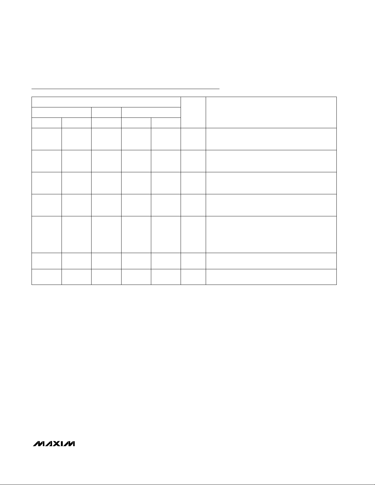
DC ELECTRICAL CHARACTERISTICS
(V+ = +5V, V- = -5V, V
LOAD
= +5V (internal load resistors on), V
IN_
= V
AGND
= V
DGND
= 0, TA= T
MIN
to T
MAX
, unless otherwise noted.
Typical values are at T
A
= +25°C.)
Stresses beyond those listed under “Absolute Maximum Ratings” may cause permanent damage to the device. These are stress ratings only, and functional
operation of the device at these or any other conditions beyond those indicated in the operational sections of the specifications is not implied. Exposure to
absolute maximum rating conditions for extended periods may affect device reliability.
PARAMETER CONDITIONS MIN TYP MAX UNITS
MAX4359/MAX4360
20 32
Offset Voltage Drift 20 µV/°C
Buffer Offset Voltage
TA= +25°C ±1 ±15
Supply Current, All Buffers On
(no external load)
37
mA
Supply Current, All Buffers Off 1.6 5 mA
Power-Supply Rejection Ratio ±4.5V to ±5.5V 50 64 dB
Operating Supply Voltage Inferred from PSRR test ±4.5 ±5.5 V
0.99 1.0 1.01
Voltage Gain V/V
Analog Input Current ±0.1 ±100 nA
Output Leakage Current Internal load resistors off, all buffers off ±100 nA
TA= T
MIN
to T
MAX
±20
mV
V
LOAD
= 5V
250 400 600
Internal Amplifier Load Resistor
200 765
Ω
Digital Input Current ±1
Output Impedance at DC 10 Ω
Input Logic Low Threshold 0.8 V
Input Logic High Threshold 2.4 V
0.4
4
V
Serial mode,
V
SER/PAR
= 5V
µA
Buffer Output Voltage Swing Internal load resistors on, no external load ±1.3 V
Total Supply Voltage (V+ to V-) ...........................................+12V
Positive Supply Voltage (V+) Referred to AGND .......-0.3V to +12V
Negative Supply Voltage (V-) Referred to AGND ......-12V to +0.3V
DGND to AGND ..................................................................±0.3V
Buffer Short Circuit to Ground when
Not Exceeding Package Power Dissipation .............Indefinite
Analog Input Voltage ............................(V+ + 0.3V) to (V- - 0.3V)
Digital Input Voltage .............................(V+ + 0.3V) to (V- - 0.3V)
Input Current, Power On or Off
Digital Inputs.................................................................±20mA
Analog Inputs ...............................................................±50mA
Continuous Power Dissipation (T
A
= +70°C)
36-Pin SSOP (derate 11.8mW/°C above +70°C) ...........941mW
24-Pin SO (derate 11.8mW/°C above +70°C)................941mW
40-Pin Plastic DIP (derate 11.3mW/°C above +70°C)....889mW
44-Pin PLCC (derate 13.3mW/°C above +70°C) .......1066mW
Operating Temperature Ranges
MAX4456C _ _ ....................................................0°C to +70°C
MAX4_ _ _E_ _ .................................................-40°C to +85°C
Junction Temperature......................................................+150°C
Storage Temperature Range .............................-65°C to +150°C
Lead Temperature (soldering, 10sec) .............................+300°C
ABSOLUTE MAXIMUM RATINGS
Internal load resistors on,
no external load, V
IN
= 0 to 1V
IOL= 0.4mA
IOH= -0.4mA
TA= +25°C
TA= T
MIN
to T
MAX
0.98 1.0 1.02
Input Voltage Range Inferred from swing test -1.3 1.3 V
SER OUT Output Logic Low/High
MAX4456
39 50
65TA= T
MIN
to T
MAX
TA= +25°C
TA= T
MIN
to T
MAX
TA= +25°C
TA= T
MIN
to T
MAX
TA= +25°C
Page 3
MAX4359/MAX4360/MAX4456
Low-Cost 4x4, 8x4, 8x8
Video Crosspoint Switches
_______________________________________________________________________________________ 3
Note 1: See Dynamic Test Circuits section.
Note 2: 3dB typical crosstalk improvement when R
S
= 0.
Note 3: Input test signal: 3.58MHz sine wave of amplitude 40IRE superimposed on a linear ramp (0 to 100IRE). IRE is a unit of
video-signal amplitude developed by the International Radio Engineers. 140IRE = 1.0V.
Note 4: Guaranteed by design.
PARAMETER
CONDITIONS MIN TYP MAX UNITS
All-Hostile Crosstalk 5MHz, VIN= 2Vp-p (Notes 1, 2) 57 dB
Output-Buffer Slew Rate
X
Internal load resistors on, 10pF load 250 V/µs
Single-Channel Crosstalk 5MHz, VIN= 2Vp-p (Note 1) 70 dB
All-Channel Off-Isolation 5MHz, VIN= 2Vp-p (Note 1) 80 dB
-3dB Bandwidth 10pF load, VIN= 2Vp-p (Note 1) 35 MHz
Differential Phase Error (Note 3) 1.0 degrees
Differential Gain Error (Note 3) 0.5 %
Input Noise DC to 40MHz 0.3 mV
RMS
Input Capacitance All buffer inputs grounded 6 pF
Buffer Input Capacitance
Additional capacitance for each output buffer
connected to channel input
2 pF
Output Capacitance Output buffer off 7 pF
PARAMETER
Latch Delay
SYMBOL MIN TYP MAX
t
D
80
UNITS
ns
Switch Break-Before-Make Delay t
ON - tOFF
15 ns
LATCH Edge to Switch Off t
OFF
35 ns
LATCH Edge to Switch On t
ON
50 ns
Write Pulse Width Low t
WL
80 ns
Chip-Enable to Write Setup t
CE
0 ns
Write Pulse Width High t
WH
80 ns
240
Data Hold t
DH
0 ns
Latch Pulse Width t
L
80 ns
CONDITIONS
LATCH on
Parallel mode
Serial mode
Data Setup t
DS
160
ns
SWITCHING CHARACTERISTICS
(Figure 4, V+ = +5V, V- = -5V, V
LOAD
= +5V (internal load resistors on), V
IN_
= V
AGND
= V
DGND
= 0, TA = T
MIN
to T
MAX
, unless other-
wise noted. Typical values are at T
A
= +25°C.) (Note 4)
AC ELECTRICAL CHARACTERISTICS
(V+ = +5V, V- = -5V, V
LOAD
= +5V (internal load resistors on), V
AGND
= V
DGND
= 0, TA= +25°C, unless otherwise noted.)
Small-Signal -3dB Bandwidth 10pF load, VIN= 100mVp-p (Note 1) 65 MHz
0.1dB Bandwidth 10pF load, VIN= 100mVp-p (Note 1) 4 MHz
DYNAMIC SPECIFICATIONS
Page 4
MAX4359/MAX4360/MAX4456
Low-Cost 4x4, 8x4, 8x8
Video Crosspoint Switches
4 _______________________________________________________________________________________
Pin Description
2 2 2
Parallel Data Bit D0 when SER/PAR = GND. Serial
input when SER/PAR = V
CC
.
3, 5 3, 5 3, 5 Output Buffer Address Lines
4, 6, 8, 10 4, 6, 8, 10
4, 6, 8, 10,
12, 14, 16,
18
Video Input Lines
7 7 7
Asynchronous Control Line. When LOAD = VCC, all the
400Ω internal active loads are on. When LOAD = GND,
external 400Ω loads must be used. The buffers must
have a resistive load to maintain stability.
9 9 9
Digital Ground. DGND pins must have the same
potential and be bypassed to AGND. DGND should
be within ±0.3V of AGND.
11 11 11
When this control line is high, the 2nd-rank registers
are loaded with the rising edge of LATCH. If this control line is low, the 2nd-rank registers are transparent
when LATCH is low, passing data directly from the
1st-rank registers to the decoders.
—
12–16, 18,
22–26
22–26 No connection. Not internally connected.
12 17 17
Connect to VCCfor serial mode; connect to GND for
parallel mode.
13 19, 30 19, 30
Negative Supply. All V- pins must be connected to each
other and bypassed to GND separately (Figure 2).
14 20 20
In serial mode, WR (write) shifts data into the input register. In parallel mode, WR loads data into the 1st-rank
registers. Data is latched on the rising edge.
1 21 1 1
Parallel Data Bit D1 when SER/PAR = GND. Serial output for cascading multiple parts when SER/PAR = V
CC
.
D1/
SER OUT
2 3
3, 4, 6 4, 5, 7
5, 7, 9, 11,
13, 15, 17,
19
6, 8, 10, 13,
15, 17, 19,
21
8 9
10, 12 11, 14
14 16
—
1, 12, 23,
34
18 20
20, 34 22, 38
21 24
D0/SER IN
A_
IN_
LOAD
DGND
EDGE/
LEVEL
N.C.
SER/PAR
V-
WR
MAX4360 MAX4456MAX4359
DIP PLCCSO SSOP SSOP
FUNCTIONNAME
PIN
15 21 21
If EDGE/LEVEL = VCC, data is loaded from the 1strank registers to the 2nd-rank registers on the rising
edge of LATCH. If EDGE/LEVEL = GND, data is
loaded while LATCH = GND. In addition, data is
loaded during the execution of parallel-mode functions 1011 through 1110, or if LATCH = V
CC
during
the execution of the parallel-mode “software-latch”
command (1111).
22 25 LATCH
Page 5
MAX4359/MAX4360/MAX4456
Low-Cost 4x4, 8x4, 8x8
Video Crosspoint Switches
_______________________________________________________________________________________ 5
Pin Description (continued)
V+
D2
D3
AGND
OUT_
CE
CE
18, 29, 4416, 26, 40
4238
4036
31, 33, 3628, 30, 32
28, 30, 32,
35, 37, 39,
41, 43
25, 27, 29,
31, 33, 35,
37, 39
2724
2623
Positive Supply. All V+ pins must be connected to each
other and bypassed to AGND separately (Figure 2).
13, 363624
Parallel Data Bit D2 when SER/PAR = GND. Not used
when SER/PAR = V
CC
.
343422
Parallel Data Bit when SER/PAR = GND. When
D3 = GND, D0–D2 specify the input channel to be connected to specified buffer. When D3 = V
CC
, D0–D2
specify control codes. D3 is not used in serial mode
(SER/PAR = V
CC
).
323220
Analog Ground. AGND must be at 0.0V, since the gainsetting resistors of the buffers are connected to these
pins.
15, 292918
Buffer Outputs. Buffer inputs are internally grounded with
a 1000 or 1001 command from the D3–D0 lines.
28, 31, 33,
35
28, 31, 33,
35
17, 19, 21,
23
Active-High Chip Enable. WR is enabled when
CE = GND and CE = V
CC
. WR is disabled when
CE = V
CC
and CE = GND.
272716
Active-Low Chip Enable. WR is enabled when
CE = GND and CE = V
CC
. WR is disabled when
CE = V
CC
and CE = GND.
———
PLCCDIPSSOPSSOPSO
NAME
PIN
FUNCTION
MAX4456MAX4360MAX4359
Page 6

MAX4359/MAX4360/MAX4456
Low-Cost 4x4, 8x4, 8x8
Video Crosspoint Switches
6 _______________________________________________________________________________________
Detailed Description
Output Buffers
The MAX4456 video crosspoint switch consists of 64
T-switches in an 8x8 grid (Figure 1). The eight matrix
outputs are followed by eight wideband buffers optimized for driving 400Ω and 20pF loads. The
MAX4359’s core is a 4x4 switch matrix with each of its
outputs followed by a wideband buffer. The MAX4360
has an 8x4 matrix and four output buffers. Each buffer
has an internal active load on the output that can be
readily shut off through the LOAD input (off when LOAD
= 0V). The shut-off is useful when two or more crosspoints are connected in parallel to create more input
channels. With more input channels, only one set of
buffers can be active and only one set of loads can be
driven. When active, the buffer must have either 1) an
internal load, 2) the internal load of another buffer in
another MAX4359/MAX4360/MAX4456, or 3) an external load.
Each output can be disabled under logic control. When
a buffer is disabled, its output enters a high-impedance
state. In multichip parallel applications, the disable
function prevents inactive outputs from loading lines
driven by other devices. Disabling the inactive buffers
reduces power consumption.
The outputs connect easily to MAX497 quad, gain-oftwo buffers when back-terminated 75Ω coaxial cable
must be driven.
Figure 1. MAX4456 Functional Diagram
IN1 IN2 IN3
IN0
IN4 IN5
MAX4456
8x8
SWITCH
MATRIX
IN6 IN7
OUTPUT
BUFFERS
A = +1
OUT0
400Ω
LOAD
A = +1
AGND
LATCH
EDGE/LEVEL
WR
CE
CE
DGND
2nd-RANK REGISTERS
SER/PAR
A1
A0
D0/SER IN
A2
1st-RANK REGISTERS
D3
D2
D1/SER OUT
V-
V+
OUT7
400Ω
Page 7

MAX4359/MAX4360/MAX4456
Low-Cost 4x4, 8x4, 8x8
Video Crosspoint Switches
_______________________________________________________________________________________ 7
Power-On RESET
The MAX4359/MAX4360/MAX4456 have an internal
power-on reset (POR) circuit that remains low for 5µs
after power is applied. POR also remains low if the total
supply voltage is less than 4V. The POR disables all
buffer outputs at power-up, but the switch matrix is
not preset to any initial condition. The desired switch
state should be programmed before the buffer outputs
are enabled.
Digital Interface
The desired switch state can be loaded in a parallelinterface mode or serial-interface mode (Table 3 and
Figures 4, 5, 6). All action associated with the WR line
occurs on its rising edge. The same is true for the
LATCH line if EDGE/LEVEL is high. Otherwise, the second-rank registers update while LATCH is low (when
EDGE/LEVEL is low). WR is logically ANDed with CE
and CE (when present) to allow active-high or activelow chip enable.
6-Bit Parallel-Interface Mode
(MAX4359/MAX4360)
In the MAX4359/MAX4360’s parallel-interface mode
(SER/PAR = GND), the six data bits specify an output
channel (A1, A0) and the input channel to which it connects (D3–D0). This data is loaded on the rising edge
of WR. The input channels are selected by codes 0000
through 0111 (D3–D0) for the MAX4360, and codes
0000 through 0011 (D3–D0) for the MAX4359. Note that
the MAX4359 does not use codes 0100 through 0111.
The eight codes 1000 through 1111 control other functions, as listed in Table 1.
7-Bit Parallel-Interface Mode (MAX4456)
In the MAX4456’s parallel-interface mode (SER/PAR =
GND), the seven data bits specify an output channel
(A2, A1, A0) and the input channel to which it connects
(D3–D0). This data is loaded on the rising edge of WR.
The input channels are selected by codes 0000
through 0111 (D3–D0) for the MAX4456. The remaining
eight codes 1000 through 1111 control other functions,
as listed in Table 1.
16-Bit Serial-Interface Mode
(MAX4359/MAX4360)
In serial mode (SER/PAR = VCC), all first-rank registers
are loaded with data, making it unnecessary to specify
an output address (A1, A0). The input data format is
D3–D0, starting with OUT0 and ending with OUT3 for
16 total bits. For the MAX4360, only codes 0000
through 1010 are valid. For the MAX4359, only the
codes 0000 through 0011 and codes 1000 through
1010 are valid. Code 1010 disables a buffer, while
code 1001 enables it. After data is shifted into the 16bit first-rank register, it is transferred to the second rank
by LATCH (Table 2), which updates the switches.
Table 1. Parallel-Interface Mode Functions
For the MAX4359, unused codes.0100 and 0111
Do not use these codes in the parallel-interface mode. These codes are for the serialinterface mode only.
1001 and 1010
Send a pulse to the 2nd-rank registers to load them with the contents of the 1st-rank
registers. When latch is held high, this “software-LATCH” command performs the same
function as pulsing LATCH low.
1111
Turn on all buffers, and restore the connected channels.1110
Turn off all buffers, and leave 2nd-rank registers unchanged.1101
Turn on the buffer selected by A2–A0 (MAX4456) or A1–A0 (MAX4359/MAX4360, and
restore the previously connected channel.
1100
Shut off the buffer selected by A2–A0 (MAX4456) or A1–A0 (MAX4359/MAX4360) and
retain 2nd-rank registers contents.
1011
Connect the buffer selected by A2–A0 (MAX4456) or A1–A0 (MAX4359/MAX4360) to
DGND. Note, if the buffer output is on, its output is its offset voltage.
1000
Connect the buffer selected by A2–A0 (MAX4456) or A1–A0 (MAX4359/MAX4360) to the
input channel selected by D3–D0.
0000 to 0111
FUNCTIOND3–D0A2, A1, A0
Selects
Output
Buffer
Page 8

MAX4359/MAX4360/MAX4456
Low-Cost 4x4, 8x4, 8x8
Video Crosspoint Switches
8 _______________________________________________________________________________________
32-Bit Serial-Interface Mode (MAX4456)
In serial mode (SER/PAR = VCC), all first-rank registers
are loaded with data, making it unnecessary to specify
an output address (A2, A1, A0). The input data format
is D3–D0, starting with OUT0 and ending with OUT7 for
32 total bits. Only codes 0000 through 1010 are valid.
Code 1010 disables a buffer, while code 1001 enables
it. After data is shifted into the 32-bit first-rank register, it
is transferred to the second rank by LATCH (Table 2),
which updates the switches.
SERIAL /
PARALLEL
D3
H X
L
H
L
(A2), A1,
A0
X
Output
Buffer
Address
Output
Buffer
Address
D1
Serial
Output
Parallel
Input
Parallel
Input
D2
X
Parallel
Input
Parallel
Input
D0
Serial Input
Parallel
Input
Parallel
Input
COMMENT
Serial Mode
Parallel Mode,
D0–D2 = Control Code
Parallel Mode,
D0–D2 = Input Address
L
Table 3. Input/Output Line Configurations
X = Don’t care, H = 5V, L = 0V
( ) are for MAX4456 only.
Table 2. Serial-Interface Mode Functions
D3–D0 FUNCTION
0000 to 0111
Connect the selected buffer to the input
channel selected by D3–D0. Note that 0100
through 0111 are not valid for the MAX4359.
1000
Connect the input of the selected buffer to
GND. Note: If the buffer output remains
on, its input is its offset voltage.
1001
Turn on the selected buffer and connect
its input to GND. Use this code to turn on
buffers after power is applied. The default
power-up state is all buffers disabled.
1010
Shut off the selected buffer at the specified channel, and erase data stored in the
2nd rank of registers. The 2nd rank now
holds the command word 1010.
1011 to 1111
Do not use these codes in the serial-interface mode. They inhibit the latching of the
2nd-rank registers, which prevents proper
data loading.
Page 9

MAX4359/MAX4360/MAX4456
Low-Cost 4x4, 8x4, 8x8
Video Crosspoint Switches
_______________________________________________________________________________________ 9
Figure 2. MAX4456 (plastic DIP) Typical Application Circuit
Typical Application
Figure 2 shows a typical application of the MAX4456
(PDIP) with MAX497 quad, gain-of-two buffers at the
outputs to drive 75Ω loads. This application shows the
MAX4456 digital-switch control interface set up in the 7bit parallel mode. The MAX4456 uses seven data lines
and two control lines (WR and LATCH). Two additional
lines may be needed to control CE and LOAD when
using multiple MAX4456s.
The input/output information is presented to the chip at
A2, A1, A0, and D3–D0 by a parallel printer port. The
data is stored in the 1st-rank registers on the rising
edge of WR. When the LATCH line goes high, the
switch configuration is loaded into the 2nd-rank registers, and all eight outputs enter the new configuration at
the same time. Each 7-bit word updates only one output buffer at a time. If several buffers are to be updated, the data is individually loaded into the 1st-rank registers. Then, a single LATCH pulse is used to reconfigure all channels simultaneously.
The short BASIC program in Figure 3 loads programming data into the MAX4456 from any IBM PC or compatible. It uses the computer’s “LPT1” output to interface
to the circuit, then automatically finds the address for
LPT1 and displays a table of valid input values to be
used. The program does not keep track of previous
commands, but it does display the last data sent to
LPT1, which is written and latched with each transmission. A similar application is possible with the
MAX4359/MAX4360.
Chip Information
MAX4359 TRANSISTOR COUNT: 2372
MAX4360 TRANSISTOR COUNT: 2372
MAX4456 TRANSISTOR COUNT: 3820
MAX497
5
IN0
7
IN1
9
8 INPUT
VIDEO
CHANNELS
14
18
19
20
21
22
23
24
25
1
2
3
4
5
6
7
8
11
13
15
17
19
22
21
2
1
38
36
6
4
3
IN2
IN3
IN4
IN5
MAX4456
IN6
IN7
LATCH
WR
D0/SER IN
D1/SER OUT
D2
D3
A0
A1
A2
EDGE/LEVEL
OUT0
OUT1
OUT2
OUT3
OUT4
OUT5
OUT6
OUT7
LOAD
AGND
DGND
SER/PAR
CE
V+
V+
VV-
CE
V+
39
37
35
33
31
29
27
25
24
14
8
40
26
28, 30, 32
10, 12
20
34
23
18
16
2
4
6
8
9,15
+5V
IN0 OUT0
= 2
A
IN1
IN2
IN3
V
CC
V
OUT1
OUT2
OUT3
GND
1, 3, 5, 7
+5V
-5V
V
16
14
12
10
EE
11,13
75Ω
-5V
Z0 = 75Ω
75Ω
DB–25
NOTE: ALL BYPASS CAPACITORS ARE 0.1µF CERAMIC.
Page 10

MAX4359/MAX4360/MAX4456
Low-Cost 4x4, 8x4, 8x8
Video Crosspoint Switches
10 ______________________________________________________________________________________
Timing Diagrams
Figure 3. BASIC Program for Loading Data into the MAX4456 from a PC Using Figure 2’s Circuit
Figure 4. Write Timing for Serial- and Parallel-Interface Modes
A0–A2
VALID DATA N-1 VALID DATA N
D0–D3
WR
LATCH
t
DS
t
WL
t
DH
t
WH
t
D
t
L
Page 11

MAX4359/MAX4360/MAX4456
Low-Cost 4x4, 8x4, 8x8
Video Crosspoint Switches
______________________________________________________________________________________ 11
Timing Diagrams (continued)
Figure 5. Parallel-Interface Mode Format (SER/
PAR
= GND)
Figure 6. Serial-Mode Interface Format (SER/
PAR
= VCC)
NOTE: SEE FIGURE 4 FOR WR AND LATCH TIMING.
WR
LATCH
1st-RANK REGISTER DATA
2nd-RANK REGISTER DATA
(EDGE/LEVEL = GND)
2nd-RANK REGISTER DATA
(EDGE/LEVEL = V
)
CC
NOTES: SEE TABLE 2 FOR INPUT DATA.
SEE FIGURE 4 FOR WR AND LATCH TIMING.
DATA (N) DATA (N + 1) DATA (N + 2)
DATA (N)
DATA (N)
DATA (N)
DATA (N + 1)
DATA (N + 1)
DATA (N + 2)
DATA (N + 1)
INPUT DATA FOR OUT0
0D3 0D2 0D1 0D0 1D3 1D2 7D3 7D2 7D1 7D0
WR
LATCH
2nd-RANK REGISTER DATA
(EDGE/LEVEL = GND)
2nd-RANK REGISTER DATA
(EDGE/LEVEL = V
)
CC
INPUT DATA FOR OUT1 TO OUT6
INPUT DATA FOR OUT7
DATA VALID
DATA VALID
Page 12

MAX4359/MAX4360/MAX4456
Low-Cost 4x4, 8x4, 8x8
Video Crosspoint Switches
12 ______________________________________________________________________________________
Note 1: Connect LOAD to +5V (internal 400Ω loads on at all outputs).
Note 2: Program any one input to connect to any one output. See Table 1 or 2 for programming codes.
Note 3: Turn on the buffer at the selected output (Table 1 or 2).
Note 4: Drive the selected input with V
IN
, and measure V
OUT
at the -3dB frequency at the selected output.
Note 5: Program each numbered input to connect to the same numbered output (IN0 to OUT0, IN1 to OUT1, etc., for the MAX4456;
also IN4 to OUT0, IN5 to OUT1, etc., for the MAX4360.) See Table 1 or 2 for programming codes.
Note 6: Turn off all output buffers (Table 1 or 2).
Note 7: Drive all inputs with V
IN
, and measure V
OUT
at any output.
Note 8: Isolation (in dB) = 20log
10(VOUT/VIN
).
Note 9: Turn on all output buffers (Table 1 or 2).
Note 10: Drive any one input with V
IN
, and measure V
OUT
at any undriven output.
Note 11: Crosstalk (in dB) = 20log
10(VOUT/VIN
).
Note 12: Drive all but one input with V
IN
, and measure V
OUT
at the undriven output.
Dynamic Test Circuits
IN0
IN1
IN2
IN3
MAX4456
IN4
IN5
IN6
IN7
VIN = 2Vp-p, SWEEP FREQUENCY
R
= 75Ω
S
OUT0
OUT1
OUT2
OUT3
OUT4
OUT5
OUT6
OUT7
LOAD
+5V
V
OUT
-3dB BANDWIDTH (NOTES 1–4) ALL-CHANNEL OFF-ISOLATION (NOTES 1, 5–8)
IN0
IN1
IN2
7 x 75Ω
IN3
IN4
IN5
IN6
IN7
MAX4456
OUT0
OUT1
OUT2
OUT3
OUT4
OUT5
OUT6
OUT7
LOAD
+5V
V
OUT
V
OUT
V
OUT
V
OUT
V
OUT
V
OUT
V
OUT
75Ω
IN0
IN1
IN2
IN3
MAX4456
IN4
IN5
IN6
IN7
= 2Vp-p AT 5MHz
V
IN
= 75Ω
R
S
IN0
IN1
IN2
IN3
MAX4456
IN4
IN5
IN6
IN7
OUT0
OUT1
OUT2
OUT3
OUT4
OUT5
OUT6
OUT7
LOAD
OUT0
OUT1
OUT2
OUT3
OUT4
OUT5
OUT6
OUT7
LOAD
V
V
V
V
V
V
V
V
+5V
V
+5V
OUT
OUT
OUT
OUT
OUT
OUT
OUT
OUT
OUT
V
V
= 2Vp-p AT 5MHz
IN
= 75Ω
R
S
= 2Vp-p AT 5MHz
IN
R
= 75Ω
S
ALL-HOSTILE CROSSTALK (NOTES 1, 5, 9, 11, 12)SINGLE-CHANNEL CROSSTALK (NOTES 1, 5, 9–11)
Page 13

MAX4359/MAX4360/MAX4456
Low-Cost 4x4, 8x4, 8x8
Video Crosspoint Switches
______________________________________________________________________________________ 13
Pin Configurations
TOP VIEW
24
23
22
21
20
19
18
17
1
2
3
4
5
6
7
8
V+
OUT0
D2
OUT1IN0
A1
D0/SER IN
D1/SER OUT
D3
OUT2
AGND
OUT3IN2
LOAD
IN1
A0
16
15
14
13
9
10
11
12
CE
LATCH
WR
V-SER/PAR
EDGE/LEVEL
IN3
DGND
SO
MAX4359
36
35
34
33
32
31
30
29
28
27
26
25
24
23
1
2
3
4
5
6
7
8
9
10
11
12
13
14
V+
OUT0
D2
OUT1
D3
OUT2
N.C.
V-
AGND
OUT3
CE
N.C.
N.C.
N.C.
N.C.
N.C.
N.C.
EDGE/LEVEL
IN3
DGND
IN2
LOAD
IN1
A0
IN0
A1
D0/SER IN
D1/SER OUT
SSOP
MAX4359
22
21
20
19
15
16
17
18 V-
N.C.
LATCH
WR
N.C.
SER/PAR
N.C.
N.C.
36
35
34
33
32
31
30
29
28
27
26
25
24
23
1
2
3
4
5
6
7
8
9
10
11
12
13
14
V+
OUT0
D2
OUT1
D3
OUT2
N.C.
V-
AGND
OUT3
CE
N.C.
N.C.
N.C.
IN5
V+
IN4
EDGE/LEVEL
IN3
DGND
IN2
LOAD
IN1
A0
IN0
A1
D0/SER IN
D1/SER OUT
SSOP
MAX4360
22
21
20
19
15
16
17
18 V-
N.C.
LATCH
WR
IN7
SER/PAR
IN6
AGND
D1/SER OUT
D0/SER IN
LOAD
EDGE/LEVEL
DGND
DGND
SER/PAR
IN0
IN1
IN2
IN3
IN4
IN5
IN6
IN7
1
2
A2
3
A1
A0
V+
V-
MAX4456
4
5
6
7
8
9
10
11
12
13
14
15
16
17
18
19
20
DIP
V+
40
OUT0
39
D2
38
OUT1
37
D3
36
OUT2
35
A1A2D0/SER IN
V-
34
OUT3
33
AGND
32
OUT4
31
AGND
30
OUT5
29
AGND
28
OUT6
27
V+
26
OUT7
25
CE
24
CE
23
LATCH
22
WR
21
A0
IN1
LOAD
IN2
DGND
N.C.
IN3
DGND
IN4
EDGE/LEVEL
IN5
IN0
6
7
8
9
10
11
12
13
14
15
16
17
19
V+
IN6
20
SER/PAR
21 2218
IN7
D1/SER OUT
MAX4456
V-
PLCC
N.C.V+OUT0D2OUT1
44
1234540414243
24
25
23
N.C.
WR
26
CE
LATCH
D3
39
OUT2
38
V-
37
OUT3
36
AGND
35
OUT4
34
N.C.
33
AGND
32
OUT5
31
AGND
30
OUT6
29
V+
28
27
CE
OUT7
Page 14

Package Information
SSOP.EPS
MAX4359/MAX4360/MAX4456
Low-Cost 4x4, 8x4, 8x8
Video Crosspoint Switches
14 ______________________________________________________________________________________
Page 15

MAX4359/MAX4360/MAX4456
Low-Cost 4x4, 8x4, 8x8
Video Crosspoint Switches
______________________________________________________________________________________ 15
Package Information (continued)
SOICW.EPS
Page 16

Maxim cannot assume responsibility for use of any circuitry other than circuitry entirely embodied in a Maxim product. No circuit patent licenses are
implied. Maxim reserves the right to change the circuitry and specifications without notice at any time.
16 ___________________Maxim Integrated Products, 120 San Gabriel Drive, Sunnyvale, CA 94086 408-737-7600
© 1999 Maxim Integrated Products Printed USA is a registered trademark of Maxim Integrated Products.
MAX4359/MAX4360/MAX4456
Low-Cost 4x4, 8x4, 8x8
Video Crosspoint Switches
Package Information (continued)
PLCC.EPS
PDIPW.EPS
 Loading...