

Datasheet MAN3R10, MAN3H40, MAN3G10, MAN3Y40, MAN3Y10 Datasheet (Fairchild Semiconductor)
...Page 1
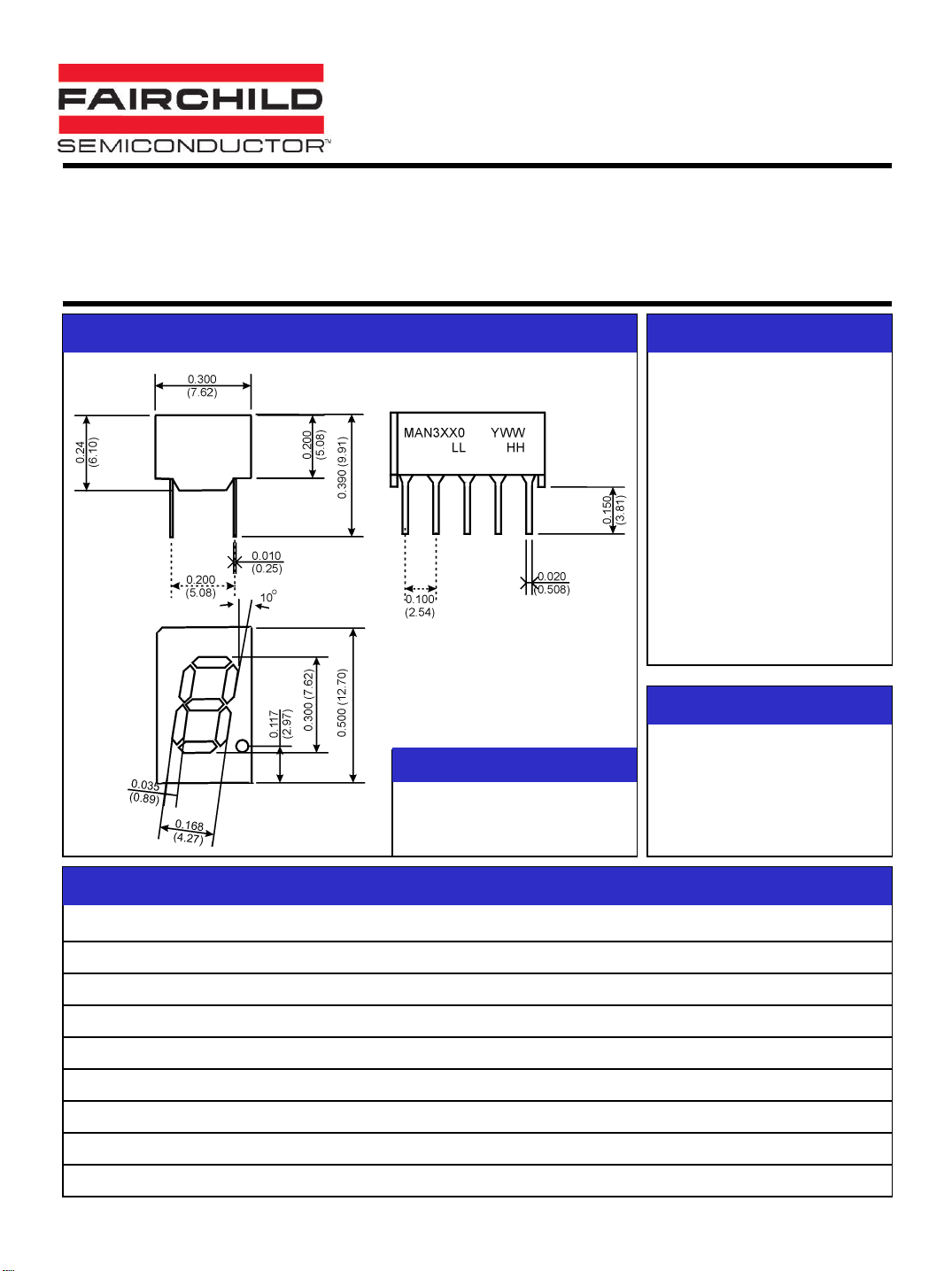
0.3 Inch (7.62mm) COMPACT
NUMERIC FRAME DISPLAY
AlInGaP Red (630nm) MAN3H10, MAN3H40
AlInGaP Red (642nm) MAN3R10, MAN3R40
AlInGaP Yellow MAN3Y10, MAN3Y40
TR/QTS/030100-001
PACKAGE DIMENSIONS FEATURES
NOTES:
•Dimensions are in inches (mm)
•Tolerances are +/- 0.010 (0.25)
unless otherwise st ated.
GaP Green MAN3G10, MAN3G40
•Bright Bold Segments
•Common Anode/Cathode
•Low Power Consumption
•Low Current Capability
•Neutral Segments
•Grey Face
•Epoxy Encapsulated
Frame
•High Performance
•High Reliability
APPLICATIONS
•Appliances
•Automotive
•Instrumentation
•Process Control
MODELS AVAILABLE
Part Number Colour Description Special
MAN3H10 AlInGaP 630nmSingle Digit, RHDP, Common Anode Low Current Capability
MAN3H40 AlInGaP 630nmSingle Digit, RHDP, Common Cathode Low Current Capability
MAN3R10 AlInGaP 642nmSingle Digit, RHDP, Common Anode Low Current Capability
MAN3R40 AlInGaP 642nmSingle Digit, RHDP, Common Cathode Low Current Capability
MAN3Y10 AlInGaP Yellow Single Digit, RHDP, Common Anode Low Current Capability
MAN3Y40 AlInGaP Yellow Single Digit, RHDP, Common Cathode Low Current Capability
MAN3G10 GaP Green Single Digit, RHDP, Common Anode Low Current Capability
MAN3G40 GaP Green Single Digit, RHDP, Common Cathode Low Current Capability
(For other colour options, contact your local area Sales Manager)
Page 2
0.3 Inch (7.62mm) COMPACT
NUMERIC FRAME DISPLAY
(1)
(T
ABSOLUTE MAXIMUM RATINGS
Part Number MAN3H10 MAN3R10 MAN3Y10 MAN3G10
Parameter MAN3H40 MAN3R40 MAN3Y40 MAN3G40 Units
= 25oC, unless otherwise specified)
A
Continuous Forward Current
25 25 25 25
mA
(each segment)
Peak Forward Current
100 100 100 100 mA
(F = 10KHz, D/F = 1/10)
Power Dissipation (P
*Derate Linearly from 25
Reverse Voltage per Die
Operating and Storage Temperature Range
Lead soldering time (1/16 inch from standoffs)
ELECTRO-OPTICAL CHARACTERISTICS
)
D
60 60 60 60 mW
o
C
0.36 0.36 0.36 0.36 mW
5 Volts
-40
5 seconds @ 230
(1)
(TA = 25oC, unless otherwise specified)
o
C to +85oC
o
C
Part Number MAN3H10 MAN3R10 MAN3Y10 MAN3G10
Parameter MAN3H40 MAN3R40 MAN3Y40 MAN3G40 Units Test Condition
Luminous intensity
Minimum ( Standard Current) 6000 4000 8000 1500 ucd I
Typical (Standard Current) 7800 5800 12800 2500 ucd I
Minimum (Low Current) 510 510 510 510 ucd I
Typical (Low Current) 1000 1000 1000 1000 ucd I
Forward Voltage (V
Typical (Standard Current) 2.05 2.05 2.05 2.05 Volts I
Maximum (Standard Current) 2.45 2.45 2.45 2.45 Volts I
Typical (Low Current) 1.80 1.80 1.80 1.80 Volts I
Maximum (Low Current) 2.20 2.20 2.20 2.20 Volts I
Peak Wavelength
Dominant Wavelength
Spectral Line 1/2 Width
(3)
Reverse B
NOTES:
(1) Data per individual LED element
(2) Luminous intensity (ucd) = average light output per segment
(3) B = breakdown
.Voltage (VR)
(2)
F
)
(IV)
632 639 591 565 nm I
624 631 585 570 nm I
20 20 20 20 nm I
5 5 5 5 Volts I
= 10mA
F
= 10mA
F
= 2mA
F
= 2mA
F
= 10mA
F
= 10mA
F
= 2mA
F
= 2mA
F
= 10mA
F
= 10mA
F
= 10mA
F
= 100uA
R
Page 3

0.3 Inch (7.62mm) COMPACT
NUMERIC FRAME DISPLAY
PIN ORIENTATION, SEGMENT IDENTI FICATION, AND PRODUCT MARKING
SCHEMATICS
Page 4

0.3 Inch (7.62mm) COMPACT
NUMERIC FRAME DISPLAY
GRAPHICAL DATA AlInGaP 630nm (TA = 25oC, unless otherwise specified)
Relative Intensity vs Case Temp. Spectral Response
Forward Current vs Forward
Voltage
Maximum Forward Current vs
Ambient Temper ature
Luminous Intensity vs Duty Cycle
Maximum Peak Current vs Duty
Cycle
Page 5

A
0.3 Inch (7.62mm) COMPACT
NUMERIC FRAME DISPLAY
GRAPHICAL DATA GaP Green (TA = 25oC, unless otherwise sp ecified)
1000
100
10
1
Forward Current [mA]
0.1
1.0 1.5 2.0 2.5 3.0 3.5 4.0
Forward Voltage [V]
1.0
0.5
@20mA
Relative Intensity
0.0
500 550 600 650 700
Wavelength [nm]
Forward Current vs Forward Voltage Spectral Response
4.0
3.5
3.0
2.5
2.0
1.5
Relative Intensity
1.0
Normalize @ 20 mA
0.5
0.0
1 10 100 1000
Forward Current [mA]
2.0
¢J
1.5
1.0
0.5
Normalize @ 25
0.0
Relative Intensity @20 mA
-40-200 20406080100
Ambient Temperat ure [ ¢J]
Relative Intensity vs Forward Current
Relative Intensity vs Ambient
Temperature
1.2
1.1
¢J
1.0
0.9
Normalize @ 25
0.8
Forward Voltage @20 m
-40 -20 0 20 40 60 80 100
Ambient Temperat ure [¢J ]
Forward Voltage vs Ambient
Temperature
Page 6

0.3 Inch (7.62mm) COMPACT
NUMERIC FRAME DISPLAY
DISCLAIMER
FAIRCHILD SEMICONDUCTOR RESERVES THE RIGHT TO MAKE CHANGES WITHOUT FURTHER NOTICE TO
ANY PRODUCTS HEREIN TO IMPROVE RELIABILITY, FUNCTION OR DESIGN. FAIRCHILD DOES NOT ASSUME
ANY LIABILITY ARISING OUT OF THE APPLICATION OR USE OF ANY PRODUCT OR CIRCUIT DESCRIBED HEREIN;
NEITHER DOES IT CONVEY ANY LICENSE UNDER ITS PATENT RIGHTS, NOR THE RIGHTS OF OTHERS.
LIFE SUPPORT POLICY
FAIRCHILD’S PRODUCTS ARE NOT AUTHORIZED FOR USE AS CRITICAL COMPONENTS IN LIFE SUPPORT DEVICES
OR SYSTEMS WITHOUT THE EXPRESS WRITTEN APPROVAL OF THE PRESIDENT OF FAIRCHILD SEMICONDUCTOR
CORPORATION. As used herein:
1. Life support devices or systems are devices or systems
which, (a) are intended for surgical implant into the body,
or (b) support or sustain life, and (c) whose failure to
perform when properly used in accordance with
instructions for use provided in the labeling, can be
reasonably expected to result in a significant injury of the
user.
2. A critical component in any component of a life support
device or system whose failure to perform can be
reasonably expected to cause the failure of the life support
device or system, or to affect its safety or effectiveness.
www.fairchildsemi.com © 2000 Fairchild Semiconductor Corporation
 Loading...