

Page 1
Digital Switched Delay Line,
1.8 - 2.4 GHz
V 1.00
MAMUSM0008
Features
n 750 pS Dynamic Range, 50 pS Step Size
n BGA Package
n Parallel Control Interface
n Positive Control Logic
n Cascadable
n No off chip components required
Description
The M/A-COM MAMUSM0008 is a 0 to 750 pS variable
delay line controlled by 4 complementary bit pairs. It
provides the user with 50 pS delay step sizes for use in
standard wireless applications. The MAMUSM0008 is
particularly useful in providing time delay in the
cancellation loops of feed-forward amplifiers.
Absolute Maximum Ratings 1
Parameter
Control Voltage 8.5V
Maximum RF Input Power +30 dBm
Operating Temperature -40°C to +85°C
Storage Temperature -55°C to +125°C
Absolute Maximum
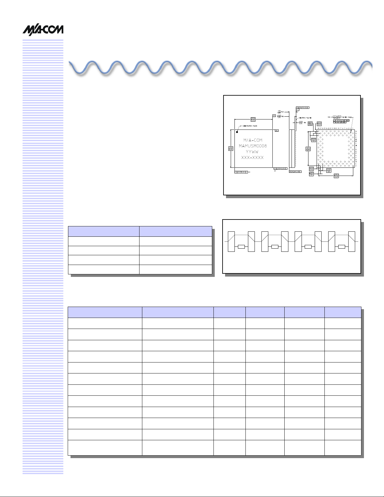
BGA Package
Block Diagram
50 ps 100 ps 200 ps 400 ps
1. TA = +25°C (unless otherwise specified)
Electrical Specifications: TA = 25°C, Z0 = 50Ω
Parameter Conditions Units Min. Typ. Max.
Frequency 1.8 - 2.4 GHz — — — —
Delay Line Control Range — pS 0 — 750
Delay Line Control Step Size — pS — 50 —
Delay Step Accuracy ± 5 pS +5% of step size in pS — — — —
Output Return Loss — dB 15 20 —
Input Return Loss — dB 15 20 —
Input P1dB — dBm 27 — —
Insertion Loss — dB 5 — 8
Output IP3 PIN = 0 dBm, 5 MHz Spacing dBm 36 38 —
Control Voltage — V 2.7 3 8.5
Control Current — µA 2 20 50
Switching Speed
(50% TTL to 90% RF)
3V Control nS — 72 100
Page 2
Digital Switched Delay Line, 1.8 - 2.4 GHz
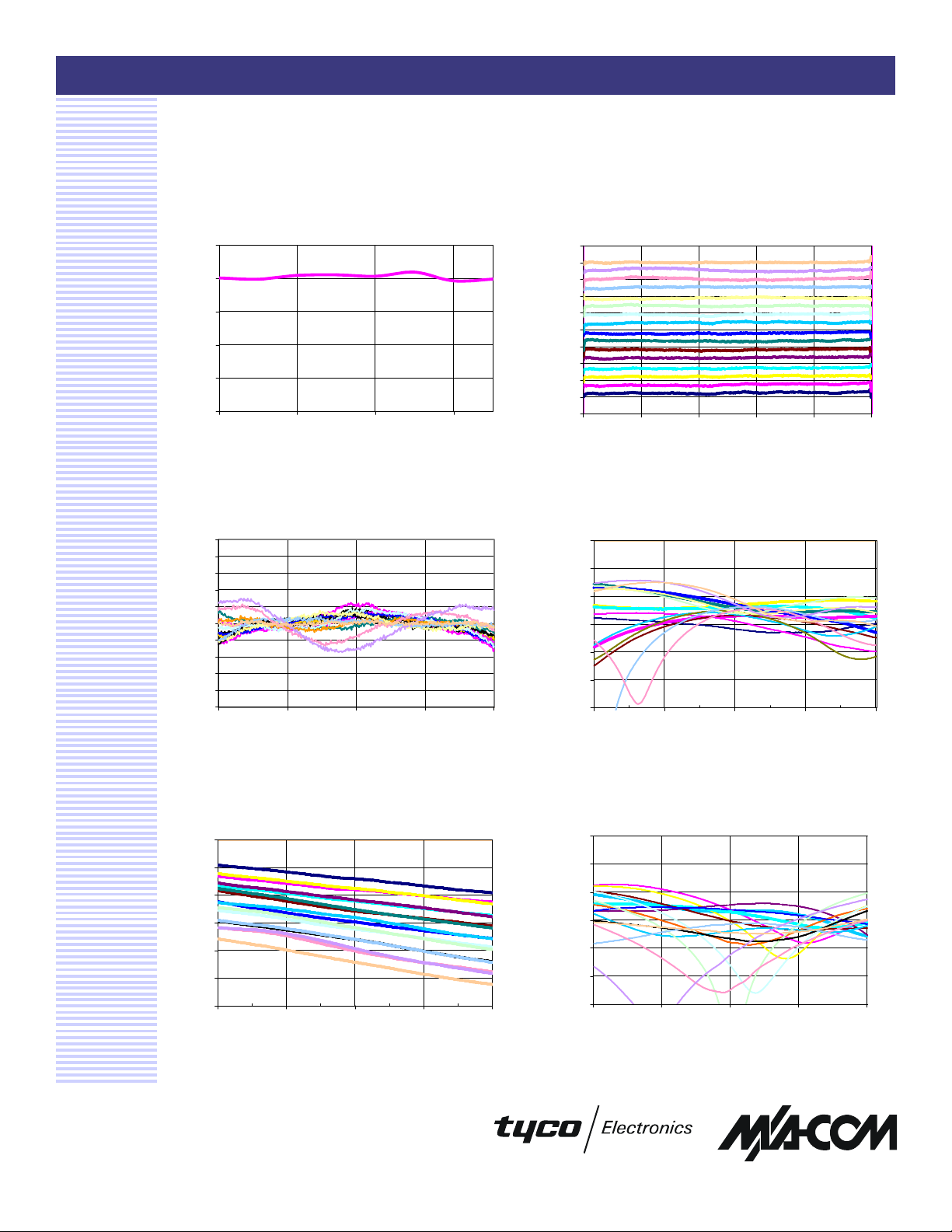
Typical Performance Curves
MAMUSM0008
V 1.00
Delay vs. Frequency OIP3 vs. Frequency
50.0
40.0
30.0
20.0
OIP3 (dBm)
10.0
0.0
1.8 2.0 2.2 2.4
Frequency (GHz)
Phase vs. Frequency
1.0
0.8
0.6
0.4
0.2
0.0
-0.2
-0.4
Phase (degrees)
-0.6
-0.8
-1.0
1.8 2.0 2.1 2.3 2.4
Frequency (GHz)
1.6E-09
1.5E-09
1.4E-09
1.3E-09
1.2E-09
1.1E-09
1.0E-09
Delay (s)
9.0E-10
8.0E-10
7.0E-10
6.0E-10
1.8 1.9 2.0 2.2 2.3 2.4
Frequency (GHz)
Input Return Loss vs. Frequency
-10
-15
-20
-25
S11 (dB)
-30
-35
-40
1.8 2.0 2.1 2.3 2.4
Frequency (GHz)
Insertion Loss vs. Frequency
-5.0
-5.5
-6.0
-6.5
IL (dB)
-7.0
-7.5
-8.0
1.80 1.95 2.10 2.25 2.40
Frequency (GHz)
Specifications subject to change without notice.
n North America: Tel. (800) 366-2266
n Asia/Pacific: Tel.+81-44-844-8296, Fax +81-44-844-8298
n Europe: Tel. +44 (1344) 869 595, Fax+44 (1344) 300 020
Visit www.macom.com for additional data sheets and product information.
Output Return Loss vs. Frequency
-10
-15
-20
-25
S22 (dB)
-30
-35
-40
1.8 2.0 2.1 2.3 2.4
Frequency (GHz)
2
Page 3

Digital Switched Delay Line, 1.8 - 2.4 GHz
Typical Performance Curves
MAMUSM0008
V 1.00
Insertion Loss vs. Frequency over
Temperature at 0 pS State
-40°C +25°C +85°C
-4.0
-5.0
-6.0
IL (dB)
-7.0
-8.0
1.8 2.0 2.1 2.3 2.4
Frequency (GHz)
Input Return Loss vs. Frequency
(+85°C)
-10
-15
-20
Insertion Loss vs. Frequency over
Temperature at 750 pS State
-40°C +25°C +85°C
-5.0
-6.0
-7.0
IL (dB)
-8.0
-9.0
-10.0
1.8 2.0 2.1 2.3 2.4
Frequency (GHz)
Output Return Loss vs. Frequency
(+85°C)
-10
-15
-20
-25
S11(dB)
-30
-35
-40
1.80 1.95 2.10 2.25 2.40
Frequency (GHz)
Specifications subject to change without notice.
n North America: Tel. (800) 366-2266
n Asia/Pacific: Tel.+81-44-844-8296, Fax +81-44-844-8298
n Europe: Tel. +44 (1344) 869 595, Fax+44 (1344) 300 020
Visit www.macom.com for additional data sheets and product information.
-25
S11(dB)
-30
-35
-40
1.8 2.0 2.1 2.3 2.4
Frequency (GHz)
3
Page 4

Digital Switched Delay Line, 1.8 - 2.4 GHz
Pin-Out Diagram
18 17 16 15 14 13 12 11 10 9 8 7 6 8 4 3 2 1
GND GND GND GND GND GND GND RF_
GND GND GND GND GND GND GND GND GND
GND CTL
CTL
_C1
GND GND GND
GND GND GND
GND GND GND
GND GND GND
GND GND GND
GND GND GND
GND GND GND
GND GND GND
GND GND GND
GND GND GND
GND CTL
GND CTL
GND GND GND GND GND GND GND GND GND
GND GND GND GND GND GND GND RF_
GND CTL
_C2
GND GND
_B2
GND CTL
_B1
_D1
GND CTL
CTL
_A2
_A1
MAMUSM0008
GND
OUT
GND GND GND
_D2
GND
GND GND GND GND
GND
IN
V 1.00
A
B
C
D
E
F
G
H
J
K
L
M
N
P
R
T
U
V
Specifications subject to change without notice.
n North America: Tel. (800) 366-2266
n Asia/Pacific: Tel.+81-44-844-8296, Fax +81-44-844-8298
n Europe: Tel. +44 (1344) 869 595, Fax+44 (1344) 300 020
Visit www.macom.com for additional data sheets and product information.
4
Page 5

Digital Switched Delay Line, 1.8 - 2.4 GHz
MAMUSM0008
V 1.00
Control
Herein is described the control method for the
MAMUSM0008 Digital Delay Line. The information will
be aimed specifically at the use of the delay line mounted
on a M/A-COM test sample board. The same theory and
Delay Line Associated Letter
50 ps A
100 ps B
200 ps C
control scheme can be applied directly to the component by
itself.
400 ps D
This product allows the insertion of a variable electrical
delay between its two ports. The control consists of four
complimentary bit pairs (8 bits total). Each pair is given a
Note that each delay line has a pair named as follows:
CTL_A1 and CTL_A2, CTL_B1 and CTL_B2,
CTL_C1 and CTL_C2, CTL_D1 and CTL_D2.
different letter, as shown in the table to the right:
D2 D1 C2 C1 B2 B1 A2 A1 hex decimal state ps delay
10101010 AA 170 0 0
10101001 A9 169 1 50
10100110 A6 166 2 100
10100101 A5 165 3 150
10011010 9A 154 4 200
10011001 99 153 5 250
10010110 96 150 6 300
10010101 95 149 7 350
01101010 6A 106 8 40
01101001 69 105 9 450
01100110 66 102 10 500
01100101 65 101 11 550
01011010 5A 90 12 600
01011001 59 89 13 650
01010110 56 86 14 700
01010101 55 85 15 750
The above table illustrates the method of controlling the bits for the desired delay in pico seconds. The hex and decimal
representations are included for programming purposes. “1” denotes 5 volts and “0” denotes 0 volts. A given delay line is set
when bits 2 and bit 1 are set to 0 and 1 respectively. The given delay line is bypassed when the bits 2 and 1 are set to 1 and 0
respectively.
The “GND” pin on the test board header must be connected to the DC supply ground.
Specifications subject to change without notice.
n North America: Tel. (800) 366-2266
n Asia/Pacific: Tel.+81-44-844-8296, Fax +81-44-844-8298
n Europe: Tel. +44 (1344) 869 595, Fax+44 (1344) 300 020
Visit www.macom.com for additional data sheets and product information.
5
Page 6

Digital Switched Delay Line, 1.8 - 2.4 GHz
MAMUSM0008
V 1.00
Measurement
The simplest way to measure the delay steps is with a vector network analyzer (VNA). For taking S-Parameter
data, perform a standard calibration and measure the parameters for the given state.
Below is a description of how to see the delay accurately.
M/A-COM recommends the following measurement procedure:
Set the delay line to the reference or insertion delay state.
With the two ports of the VNA connected to the “in” and
“out” on the test board, measuring S21, set displayà
memory, and display data/memory. This will normalize
your data to the reference insertion state.
Next, switch the measurement format to phase. This
should be flat and zero due to the normalization. Switch
in the first delay line. (50ps). The display will not remain
on zero, but will have an offset. Under the Scale/
Reference menu, select electrical delay, and dial that up
until the data reads zero again, across the band of interest.
That electrical delay will be 50ps.
Continue to switch in the delay lines, dialing in more
delay each time.
Other methods are possible, but this is the most straightforward approach. We do not recommend using the
‘delay’ format in the VNA. The VNA’s method of
measuring this results in a noisy response, and is less
accurate than the method outlined above.
Upon request, M/A-COM can provide a test control board
to ease stepping through the states.
Ordering Information
Part Number Package
MAMUSM0008 Bulk Packaging
MAMUSM0008TR Tape and Reel (1K Reel)
MAMUSM0008-TB Units Mounted on Test Board
Specifications subject to change without notice.
n North America: Tel. (800) 366-2266
n Asia/Pacific: Tel.+81-44-844-8296, Fax +81-44-844-8298
n Europe: Tel. +44 (1344) 869 595, Fax+44 (1344) 300 020
Visit www.macom.com for additional data sheets and product information.
6
 Loading...