

Datasheet MAMDCC0005-DC000, MAMDCC0002-DC000, MADRCC0002TR, MADRCC0002, SA90-0001-DC000 Datasheet (M A COM)
Page 1
Dual Linear Driver for Vector
Modulators
V 2.00
MADRCC0002
Features
n Linearizes M/A-COM’s PIN Diode Vector Modulators
Over a 360° Phase Range
n Dual Channels Allow One Driver per Vector Modulator
n Output Currents up to 12 mA
n Operates with a Single Supply Voltage of +5V
n Low Quiescent Currents
n Single Control Voltage for Each Channel
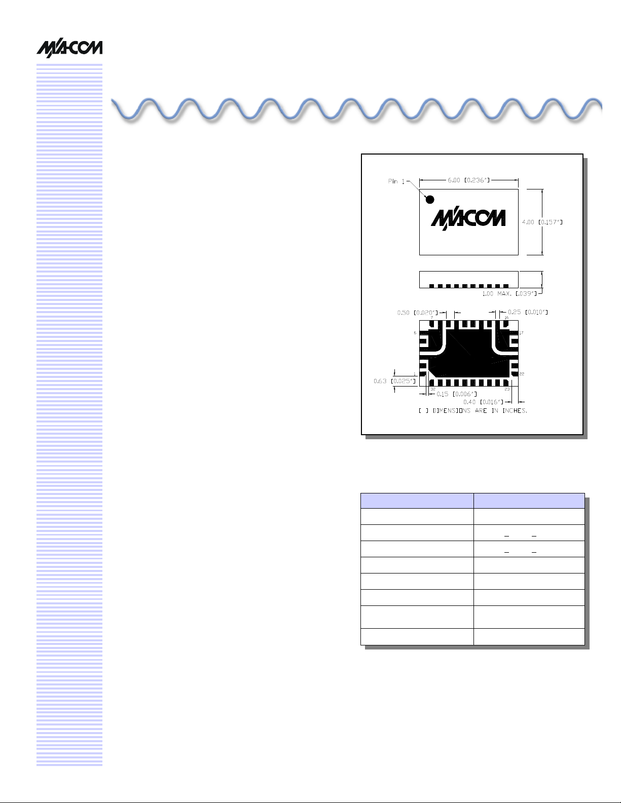
n 6 x 4 mm Chip Scale Package
n Test Boards with Vector Modulators are Available
n Tape and Reel Packaging Available
Description
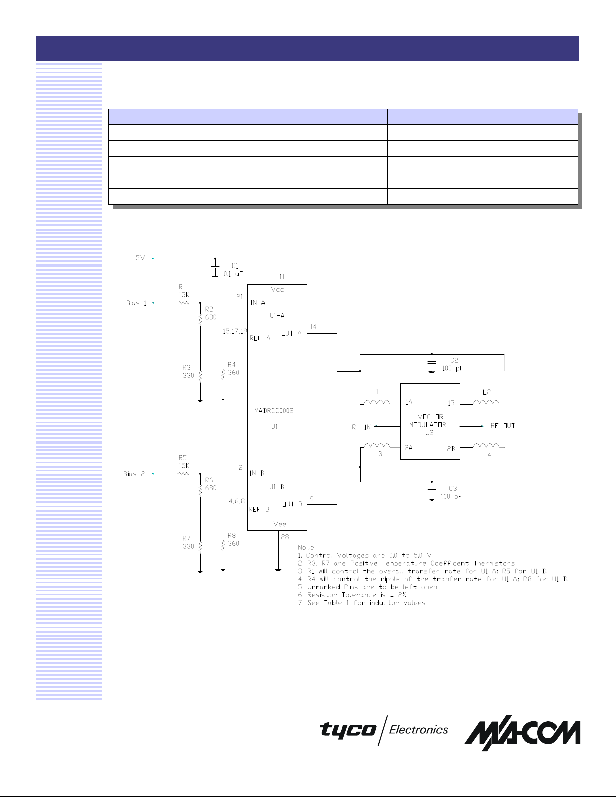
M/A-COM's MADRCC0002 is a dual, break point free
driver that produces a logarithmic output current suitable
for linearizing PIN diode based vector modulators. This
driver, in conjunction with the external components, as
defined in Figure 1, produces a linearized transfer function
between the input control voltage of the driver and the
attenuation / phase output of the vector modulator. The
MADRCC0002 has been optimized for linearizing
M/A-COM’s Vector Modulators (see Table 1), but will
function well with most types of cathode grounded vector
modulators. The driver is packaged in a 6 x 4 mm Chip
Scale Package for commercial SMT applications. A typical
schematic for a dual linearizer driving a vector modulator is
shown in Figure 1.
CSP-9
Circuit Description:
(Reference Figures 1, 2 and 3)
Note that this is a dual driver. Only the top circuit will be
described, because the bottom circuit is identical. The input
divider, R1 and the sum of R2 and R3, sets the overall
transfer function of the circuit. To increase the transfer
function, decrease the Control Voltage and the value of R1.
Temperature compensation is a function of the temperature
coefficient of the thermistor, R3, and the ratio of R2 to R3,
and can only be optimized once the transfer function and
linearity component values have been established. Varying
the value of R4 will optimize the linearity of the VVA. One
can achieve a more linear transfer function by driving the
attenuator over a smaller portion of its dynamic range. Note
that when the vector modulators called out in Table 1 are
driven with the dual linearizer, both amplitude and phase
are affected, which makes it hard to define linearity. The
individual transfer function of each voltage variable
attenuator in the vector modulator (See Figure 2 for the
block diagram) is linearized as a function of voltage. The
two VVAs in the block diagram are the quad hybrids that
are terminated by two PIN diodes. See Figure 3 for
the transfer function of the SA90-0001 vector modulator
(phase and attenuation vs. control voltages).
Absolute Maximum Ratings 1
Parameter Absolute Maximum
+V
CC
IN A, IN B -0.5V < Input < Vcc +0.5V
REF A, REF B -0.5V < Input < Vcc +0.5V
Output Short Circuit Current 20 mA
Operating Temperature -40°C to +85°C
Storage Temperature -65°C to +125°C
Package Power Dissipation
Control Voltage
Lead Temperature 300ºC for 10 seconds
1. Operation of this device above any one of these
parameters may cause permanent damage.
+20 V
150 mW
Page 2
Dual Linear Driver for Vector Modulators
Electrical Specifications, TA = +25°C, Reference Figure 1 (Each Circuit)
Parameter Test Conditions Units Min Typical Max
Output Drive Current Vcontrol = VCC mA 18 — —
+VCC Supply Range — V 4.5 5.0 5.5
IN, REF Voltage — V 0 — VCC
+VCC Quiescent Current No Load µA — 50 70
Settling Time 50% Ctl to 90%/10% RF µS — 25 —
MADRCC0002
V 2.00
Figure 1
Specifications subject to change without notice.
n North America: Tel. (800) 366-2266
n Asia/Pacific: Tel.+81-44-844-8296, Fax +81-44-844-8298
n Europe: Tel. +44 (1344) 869 595, Fax+44 (1344) 300 020
Visit www.macom.com for additional data sheets and product information.
2
Page 3

Dual Linear Driver for Vector Modulators
1.5V
2.0V
3.5V
3.5V
90°
0°
bias 2 = 0V
bias 2 = +5V
90°
0°
bias 2 = +5V
bias 2 = 0V
coefficient = 0.5
Figure 3A - Phase and Attenuation of SA90-0001, Vector Modulator Linearized with
MADRCC0002 Linearizer
MADRCC0002
V 2.00
(y)
45°
bias 1 = 0.0V
0.5V
1.0V
2.5V
3.0V
bias 1 = 5.0V
Loss = 22 dB
Loss = 17 dB
Loss = 12 dB
bias 1 = 0V
Figure 3B
(y)
bias 1 = 0V
45°
bias 2 = 5.0V
bias 2 = 0.0V
(x)
bias 1 = +5V
3.0V
2.5V
2.0V
(x)
1.5V
1.0V
0.5V
2. Tic marks on x,y axes refer to reflection coefficient in increments of 0.1V. Reflection coefficients vary from -0.5 to +0.5 on both
the x and y axes.
3. Data is for vector modulators driven by linearizers per attached schematic.
4. Inputs to the linearizers vary from 0 to 5V.
5. The phase with the inputs to both linearizers set to +5V is arbitrarily called zero degrees.
Specifications subject to change without notice.
n North America: Tel. (800) 366-2266
n Asia/Pacific: Tel.+81-44-844-8296, Fax +81-44-844-8298
n Europe: Tel. +44 (1344) 869 595, Fax+44 (1344) 300 020
Visit www.macom.com for additional data sheets and product information.
bias 1 = +5V
Reflection
3
Page 4

Dual Linear Driver for Vector Modulators
Table 1. Inductor Selection for M/A-COM Vector Modulators
Vector Modulator Frequency Range (MHz) Coil Craft P/N L1 & L2 Description of L1 & L2
MAMDCC0005 925-960 (GSM) 0603CS-68NXJBC Inductor, 68 nH, ± 5%
MAMDCC0002 1930-1990 (PCS) 0603CS-27NXJBC Inductor, 27 nH, ± 5%
SA90-0001 2040-2240 (UMTS) 0603CS-27NXJBC Inductor, 27 nH, ± 5%
Recommended PCB Layout 6
MADRCC0002
V 2.00
Specifications subject to change without notice.
n North America: Tel. (800) 366-2266
n Asia/Pacific: Tel.+81-44-844-8296, Fax +81-44-844-8298
n Europe: Tel. +44 (1344) 869 595, Fax+44 (1344) 300 020
Visit www.macom.com for additional data sheets and product information.
4
Page 5

Dual Linear Driver for Vector Modulators
Figure 2—Block Diagram
MADRCC0002
V 2.00
Vector Modulator
Ordering Information
Part Number Package
MADRCC0002 Bulk Packaging
MADRCC0002TR Tape & Reel (1K Reel)
MAMDCC0005-DC000 Test Board with Circuit per
Figure 1
(MAMDCC0005,
GSM Vector Modulator)
MAMDCC0002-DC000 Test Board with Circuit per
Figure 1
(MAMDCC0002,
PCS Vector Modulator)
SA90-0001-DC000 Test Board with Circuit per
Figure 1
SA90-0001,
UMTS Vector Modulator
Specifications subject to change without notice.
n North America: Tel. (800) 366-2266
n Asia/Pacific: Tel.+81-44-844-8296, Fax +81-44-844-8298
n Europe: Tel. +44 (1344) 869 595, Fax+44 (1344) 300 020
Visit www.macom.com for additional data sheets and product information.
Pin Configuration
Pin # Function Pin # Function
1 NC 17 REF A
2 IN B 18 NC
3 NC 19 REF A
4 REF B 20 NC
5 NC 21 IN A
6 REF B 22 NC
7 NC 23 NC
8 REF B 24 NC
9 OUT B 25 NC
10 NC 26 NC
11 Vcc 27 NC
12 NC 28 GND
13 NC 29 NC
14 OUT A 30 NC
15 REF A 31 NC
16 NC 32 NC
5
 Loading...