

Page 1
MITSUBISHI<Dig.Ana.INTERFACE>
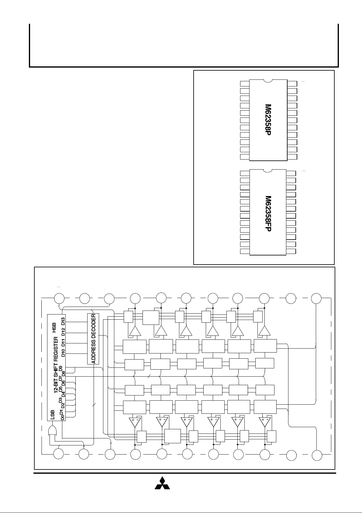
The M62358 is a 12-channel 8-bit voltage output digital to analog
converter.
The M62358 includes data latch circuit and gain change circuit
of output amplifiers.
Input data is a easy-to-use three-wires serial interface.It is able
to cascading serial use with Do terminal.
Gain set up data change a case the each channel`s output
voltage range is change ,and each channel`s output voltage
range is able to change severally make use of gain set up data.
Signal gain control of DISPLAY-MONITOR or CTV.
R-2R D-A
G
G
G
GGGGG
G
G
M62358P,FP
8-BIT 12CH D-A CONVERTER WITH BUFFER AMPLIFIERS
DESCRIPTION
FEATURES
•All channel includes gain change latch circuit with output
amplifiers.
•14-bit serial data input
•Built-in reset circuit
APPLICATION
Conversion from digital control data to analog control data
for home-use and industrial equipment.
Automatic adjustment by combination with EEPROM and
microcomputer(replacement of conventional half-fixed
resistor).
PIN CONFIGURATION (TOP VIEW)
R
LD
CLK
DI
Ao7
Ao8
Ao9
Ao10
Ao11
Ao12
GND
VrefL
LD
CLK
DI
Ao7
Ao8
Ao9
Ao10
Ao11
Ao12
NC
GND
VrefL
1
2
3
4
Outline 22P4H
1
2
3
4
Outline 24P2-E
22
VDD
21
DO
20
Ao6
19
Ao5
185
Ao4
176
Ao3
167
Ao2
158
Ao1
149
Vcc
1310
VrefU
1211
24
23
22
Ao6
21
Ao5
205
196
187
178
169
1510
1411
Vcc
1312
VrefU
NC:NO CONNECTION
R
VDD
DO
Ao4
Ao3
Ao2
Ao1
NC
BLOCK DIAGRAM
R
VDD
GAIN
CHANGE
LATCH
R-2R D-A
LATCH
12
LATCH
Ao5
-
8-BIT
8-BIT
8-BIT
8-BIT
+
Do
2
Ao6
-
R-2R
L
L
R-2R
+
GAIN
CHANGE
LATCH
Ao4
+
-
L
R-2R R-2R
Ao3
-
R-2RR-2R
LL
Ao2 Ao1
+
-
R-2R
LL
L
R-2R
+
-
R-2R
L
L
R-2R
+
Vcc
VrefU
LD
CLK
DI
Ao7
Ao8
MITSUBISHI
ELECTRIC
Ao9
Ao10
Ao11
Ao12
GND
( / 6 )
VrefL
1
Page 2
8-BIT 12CH D-A CONVERTER WITH BUFFER AMPLIFIERS
EXPLANATION OF TERMINALS
Pin No. Symbol
3
20
2
1
21
13
10
12
11
22
14
15
16
17
18
19
4
5
6
7
8
9
DI
DO
CLK
LD
VDD
Vcc
GND
VrefU
VrefL
R
Ao1
Ao2
Ao3
Ao4
Ao5
Ao6
Ao7
Ao8
Ao9
Ao10
Ao11
Ao12
*1 When the LD terminal is "H" input data has load.
Serial data input terminal
Serial data output terminal
Serial clock input terminal
LD terminal input high level than latch circuit data load *1
Digital power supply terminal
Analog power supply terminal
Digital and Analog common GND
D-A converter high level reference voltage input terminal
D-A converter low level reference voltage input terminal
Reset terminal
8-bit D-A converter output terminal
MITSUBISHI<Dig.Ana.INTERFACE>
M62358P,FP
Function
ABSOLUTE MAXIMUM RATINGS(Ta=25°C, unless otherwise noted)
Symbol
VCC
VDD
VrefU
VIN
IDO
IAO
Topr
Tstg
Parameter
Supply voltage
Supply voltage
D-A converter high level reference voltage
Input voltage
Output current -5~+5
Buffer amplifier output current range
Operating temperature
Storage temperature
Conditions
RECOMMENDED OPERATING CONDITIONS
•Digital supply voltage VDD 5V±10%
•Analog supply voltage Vcc VDD~13V
ELECTRICAL CHARACTERISTICS
Digital part(Vcc=13V,VDD=VrefU=5V, Ta=25°C,unless otherwise noted)
Symbol
VDD
IDD
VIL
VIH
VOL
VOH
Parameter
Supply voltage
Circuit current
Input low voltage
Input high voltage
Output low voltage
Output high voltage
CLK=1MHz in action
IOL=1.0mA
IOH=-400µA
Test conditions
Min.
4.5
0.8VDD
VDD-0.4
Ratings
-0.3~13.5
-0.3~7
VDD
-0.3~VDD+0.3
-5~+5
-20~+85
-40~+125
Limits
Typ.
Max.
5.5
1
0.2VDD
0.4
Unit
V
V
V
V
mA
mA
°C
°C
Unit
V
mA
V
V
V
V
MITSUBISHI
ELECTRIC
( / 6 )
2
Page 3

8-BIT 12CH D-A CONVERTER WITH BUFFER AMPLIFIERS
Analog part(Vcc=13V,VDD=VrefU=5V,Ta=-20°C~+85°C, unless otherwise noted)
Symbol
Vcc
Icc
IrefU
Parameter
Supply voltage
Circuit current
D-A converter high level reference
input current
All ch‘s set up at 107/256
Test conditions
MITSUBISHI<Dig.Ana.INTERFACE>
M62358P,FP
Min.
VDD
Limits
Typ.
3
2
Max.
13
6
4
Unit
V
mA
mA
VrefU
VrefL
VAO
IAO
DNL
NL
EZ
EF
Eo
SR
D-A converter high level reference
voltage range
D-A converter low level reference
voltage range
D-A converter output
voltage range
Buffer amplifier output current range
Differential nonlinearity
Nonrineality
Zero code error
Full scale error
Gain error
Output slew rate
TIMING CHART (MODEL)
R
IAO
=±500µA
IAO
=±1mA
Guaranteed monotonic
VrefU=4.79V
VrefL=0.95V without load
3.5
0
0.1
0.2 Vcc-0.2
-1.0
-1.5
-2
-2
-3
0.2
VDD
1.5
Vcc-0.1
±2.5
1.0
1.5
2
2
3
V
V
V
mA
LSB
LSB
LSB
LSB
%
V/µs
DI
CLK
LD
AO
MSB
D13 D12
Input data is carried out LD signal Low besides CLK signal positive edge.
CLK,LD is keep generally High level.
D11
MITSUBISHI
ELECTRIC
LSB
D0
( / 6 )
3
Page 4

MITSUBISHI<Dig.Ana.INTERFACE>
M62358P,FP
8-BIT 12CH D-A CONVERTER WITH BUFFER AMPLIFIERS
AC CHARACTERISTICS(Ta=-20~85°C,Vcc=13V,VDD=VrefU=5V, unless otherwise noted)
Symbol
tCKL
tCKH
tCR Clock rise time
tCF
tDCH
tCHD
tCHL
tLDC
tLDH
tDO
tLDD
Clock "L"pulse width
Clock "H"pulse width
Clock fall time
Data set up time
Data hold time
LD setup time
LD hold time
LD "H" pulse width
Data output delay time
D-A output setting time
Parameter
CL=100pF
Without load
Test conditions
Min Typ
Limits
200
200
60
100
200
100
100
70
Max
200
200
350
300 µs
Unit
ns
ns
ns
ns
ns
ns
ns
ns
ns
ns
TIMING CHART
CLK
DI
LD
D-A
OUTPUT
DO
OUTPUT
tCR tCF
tCKL
tDCH
tCKH
tCHD
tDO
tLDC
tLDH
tCHL
tLDD
MITSUBISHI
ELECTRIC
( / 6 )
4
Page 5

DIGITAL FORMAT
01267
•14 bit serial data
1
2
DATA
CK
•Data assignment
:GAIN set up data
(LSB)
•GAIN set up data
D8
0
1
0
1
D9
0
0
1
1
9
8
:DAC select data
K
1
1.6
1.8
2.4
10
(MSB)
DAC output range
(VrefU=5V,VrefL=0V)
MITSUBISHI<Dig.Ana.INTERFACE>
M62358P,FP
8-BIT 12CH D-A CONVERTER WITH BUFFER AMPLIFIERS
(LSB)
11 12 13
:DAC set up data
0~5V
0~8V
0~9V
0~12V
14
•DAC select data
D10 D11 D12 D13
0
0
0
0
0
0
0
0
0
1
0
1
1
0
0
1
1
1
1
1
1
1
1
1
0
0
0
0
1
1
1
1
0
0
1
1
0
0
1
1
0
0
1
1
0
0
1
1
0
1
0
1
0
1
0
1
0
1
0
1
0
1
0
1
DAC selection
Don‘t care
Ao1 selection
Ao2 selection
Ao3 selection
Ao4 selection
Ao5 selection
Ao6 selection
Ao7 selection
Ao8 selection
Ao9 selection
Ao10 selection
Ao11 selection
Ao12 selection
Don‘t care
Don‘t care
Don‘t care
•DAC set up data
(LSB)
D0
0
1
0
1
0
1
D2 D3 D4 D5 D6 D7
Ao=
(MSB)
0
0
0
0
1
1
2 X D0 + 2 X D1 + 2 X D2 +••••••••+ 2 X D6 + 2 X D7 + 1
0
0
0
0
1
1
0
0
0
0
1
1
0
0
0
0
1
1
256
0
0
0
0
1
1
MITSUBISHI
ELECTRIC
DAC voltage
1/256•(VrefU-VrefL) •K +VrefL
0
2/256•(VrefU-VrefL) •K +VrefL
0
3/256•(VrefU-VrefL) •K +VrefL
0
4/256•(VrefU-VrefL) •K +VrefL
0
255/256•(VrefU-VrefL) •K +VrefL
1
256/256•(VrefU-VrefL) •K +VrefL
1
• (VrefU - VrefL) •K + VrefL
K:Amplifiers gain
( / 6 )
5
Page 6

APPLICATION CIRCUIT
GND,about 0.1µF~1µF,because keep off effect of spark
and electric discharge etc.
MITSUBISHI<Dig.Ana.INTERFACE>
M62358P,FP
8-BIT 12CH D-A CONVERTER WITH BUFFER AMPLIFIERS
Vcc=13.5V max
5V
10µF
10µF
VDD
VrefU
LD
VCC
Ao1
Ao2
Ao3
Ao4
Ao5
Ao6
Ao7
Ao8
Ao9
Ao10
ch1
ch2
ch3
ch4
ch5
ch6
ch7
ch8
ch9
ch10
*1
MICRO
COMPUTER
This IC`s output amplifier has an advantage to capacitive
load.So it`s no problem at device action when connect
capacitor among output to GND for every noise eliminate.
CLK
D1
GND VrefL
Ao11
Ao12
ch11
ch12
*1 If be used in a cathode-ray tube sets and high voltage
sets,please connect capacitor among output to
MITSUBISHI
ELECTRIC
( / 6 )
6
 Loading...