

Page 1
8-BIT 2CH D-A CONVERTER WITH BUFFER AMPLIFIERS
GENERAL DESCRIPTION
The M62342P,FP is a CMOS 2 channel D-A converter
with output buffer amplifiers.
It can communicate with a microcontroller via few wiring
thanks to the adoption of the three-line DI,CLK,LD.
The output buffer amplifier employs AB class output with
sinking and sourcing capability of more than 1.0mA , and
an output voltage range is nearly between ground and
Vcc.
FEATURES
• 10bit serial data input (3-wire serial transfer method)
• Wide output voltage range
Nearly between ground and Vcc(0 to 5V)
• High output current drive capability
over ±1.0mA
MITSUBISHI <STD. LINEAR ICs>
M62342P,FP
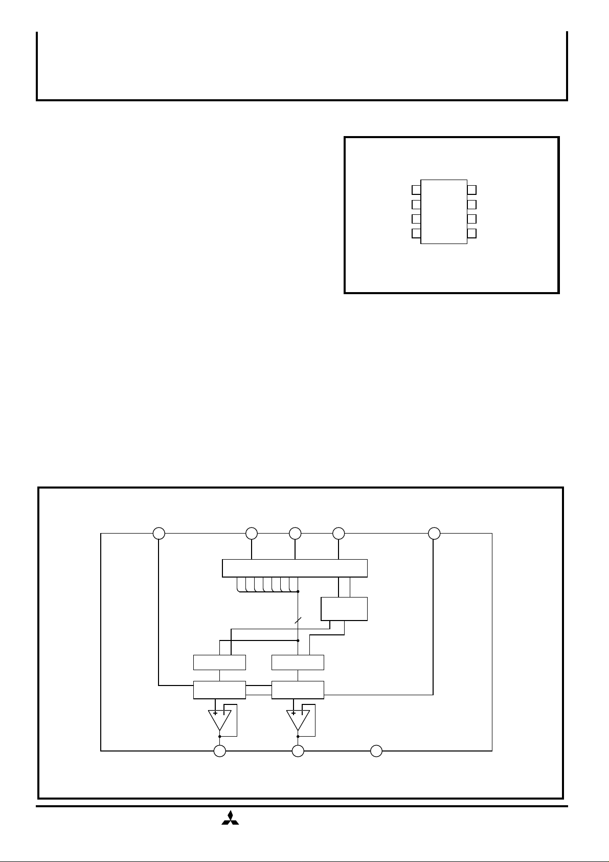
PIN CONFIGURATION (TOP VIEW)
Ao1
Ao2
N.C.
VCC
Outline
1
2
3
4
8
M62342
L D
7
CLK
6
D I
5
GND
8P4 (P)
8P2S-A (FP)
APPLICATION
Conversion from digital data to analog control data for both consumer and industrial equipment.
Gain control and automatic adjustment of DISPLAY-MONITOR or CTV.
BLOCK DIAGRAM
VCC
L D CLK
4 8 7
10-BIT SHIFT REGISTER
8bit Latch
8bit upper
segment R-2R
8bit Latch
8bit upper
segment R-2R
8
D I
6
ADDRESS
DECODER
GND
5
1
Ao1
2
Ao2
N.C.
MITSUBISHI ELECTRIC
3
2000-8-31.revB
( / 5 )
1
Page 2
EXPLANATION OF TERMINALS
PIN No.
6
Symbol
D I
Serial data input terminal
MITSUBISHI <STD. LINEAR ICs>
M62342P,FP
8-BIT 2CH D-A CONVERTER WITH BUFFER AMPLIFIERS
F u n c t i o n
7
8
1
2
4
5
CLK
L D
Ao1
Ao2
Vcc
GND
Shift clock input terminal. Input signal at DI pin is input to 10-bit shift register at
rise of shift clock pulse.
When H-level signal is input to this terminal,the value stored in 10-bit shift
register is loaded in decoder and D-A converter output register.
8bit D–A converter output terminal
Power supply terminal
GND
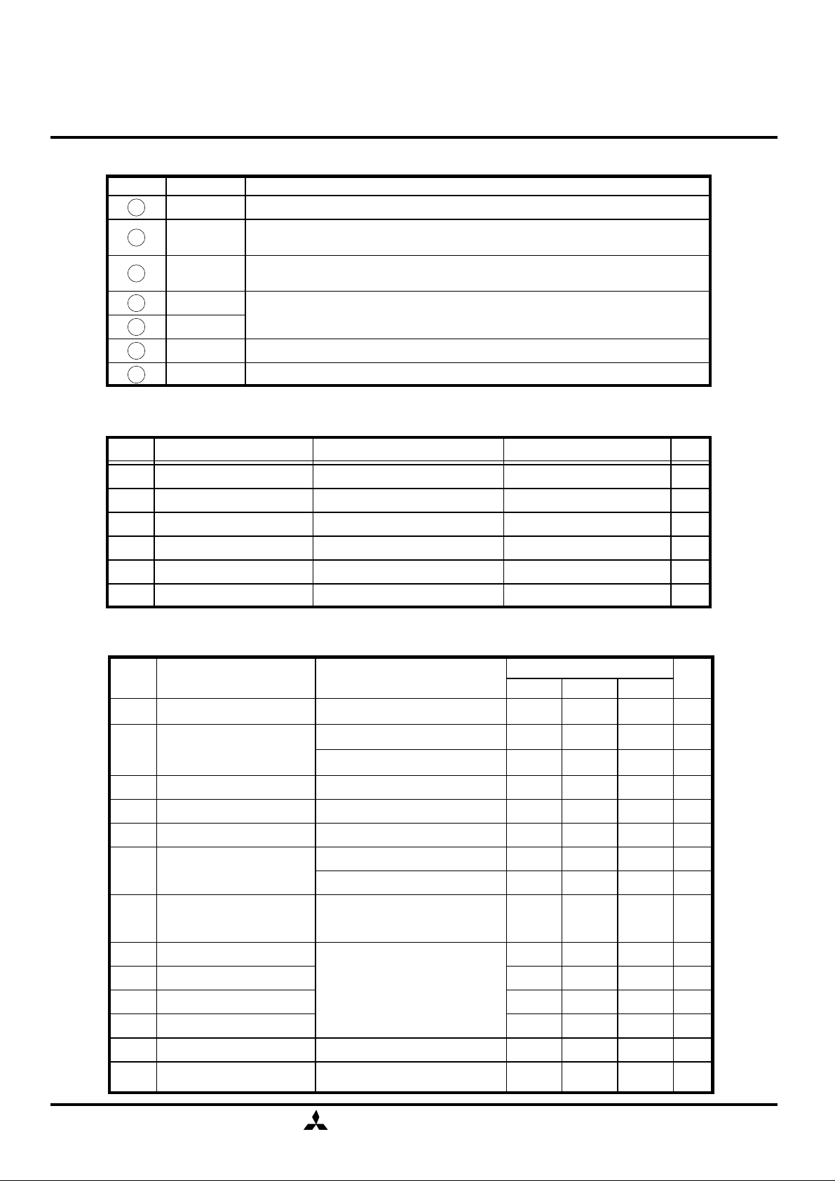
ABSOLUTE MAXIMUM RATING
Symbol
Vcc
Vin
Vo
Pd
Topr
Tstg
Parameter Conditions UnitRatings
Supply voltage
Input voltage
Output voltage
Power dissipation
Operating temperature
Storage temperature
-0.3 to 7.0
-0.3 to VCC+0.3
-0.3 to VCC+0.3
417 (DIP) / 272 (FP)
-20 to +85
-55 to +125
V
V
V
mW
°C
°C
ELECTRICAL CHARACTERISTICS (VCC=+5V±10%,GND=0V,Ta=–20 to 85°C unless otherwise noted)
Symbol
V
CC
ICC
IILK
VIL
VIH
V
AO
IAO
SDL
SL
SZERO
SFULL
Co
Ro
Parameter
Supply voltage
Supply current
Input leak current
Input low voltage
Input high voltage
Buffer amplifier output
voltage range
Buffer amplifier output
drive range
Differential nonlinearity
Nonlinearity
Zero code error
Full scale error
Output capacitive load
Buffer amplifier
output impedance
Test conditions
CLK=1MHz, IAO=0µA
DACdata:6Ah(at maximum current)
DI=CLK=LD=GND,IAO=0µA
IN=0 to VCC
V
I
AO=±100µA
I
AO=±500µA
Upper side saturation voltage=0.3V
Lower side saturation voltage=0.2V
VCC=5.12V (20mV/LSB)
without load
(IAO=0)
Min Typ Max
-10 10
0.5VCC
-1.0 1.0 mA
-1.0 1.0
-1.5 1.5
-2.0 2.0
-2.0 2.0
Ratings
2.7 5.0 5.5
0 0.7 2.5
0
0.1
0.2
0.5 1.6
0.2V
V
CC-0.1
CC-0.2
V
0.1
5.0
CC
Unit
V
mA
mA
µA
V
V
V
V
LSB
LSB
LSB
LSB
µF
Ω
MITSUBISHI ELECTRIC
2000-8-31.revB
( / 5 )
2
Page 3

MITSUBISHI <STD. LINEAR ICs>
M62342P,FP
8-BIT 2CH D-A CONVERTER WITH BUFFER AMPLIFIERS
AC CHARACTERISTICS (VCC=+5V±10%,GND=0V,Ta=–20 to 85°C unless otherwise noted)
Symbol Parameter Test condition
tCKL
tCKH
tCR
tCF
tDCH
t
CHD
tCHL
tLDC
tLDH
tLDD
Clock "L" pulse width
Clock "H" pulse width
Clock rise time
Clock fall time
Data setup time
Data hold time
LD setup time
LD hold time
LD "H" pulse time
D-A output setting time
CL≤100pF VAO:0.5V<=>4.5V
The time until the output becomes
the final value of 1/2LSB
TIMING CHART
tCR
tCKH tCF
Limits
Min Typ Max
200
200 nS
30
60
200
100
100
Unit
nS
200
300 µS
nS
nS
nS
nS
nS
nS
CLK
D I
L D
D-A
OUTPUT
tCKL
tDCH tCHD
tLDC
tLDH
tCHL
tLDD
MITSUBISHI ELECTRIC
2000-8-31.revB
( / 5 )
3
Page 4

DIGITAL DATA FORMAT
Last
LSB
MITSUBISHI <STD. LINEAR ICs>
M62342P,FP
8-BIT 2CH D-A CONVERTER WITH BUFFER AMPLIFIERS
First
MSB
D0
D1 D2
D3 D4
DAC DATA
D5
D6 D7
(1) DAC SELECT DATA
D8
0 0
0 1
1 1
D9
01
DAC selection
A
O1selection
AO2selection
Don't care
Don't care
(2) DAC DATA
D0 D1
0 0
D2 D3
0 0
D4 D5
0 0
1 0 0 0 0 0 0 0
D6 D7
0 0
D8
DAC
SELECT
DATA
DAC output
V
VCC/256 X2
D9
CC/256 X1
0 1 0 0 0 0 0 0
1 1 0 0 0 0 0 0
: :: :: ::
:
0 1 1 1 1 1 1 1
TIMING CHART (MODEL)
D I
CLK
L D
D-A
OUTPUT
D9 D8 D7 D6 D5 D2 D1 D0
VCC/256 X3
VCC/256 X4
:
CC/256 X255
V
11 1 1 1 1 1 1
VCC/256 X256
MITSUBISHI ELECTRIC
2000-8-31.revB
( / 5 )
4
Page 5

MITSUBISHI <STD. LINEAR ICs>
M62342P,FP
8-BIT 2CH D-A CONVERTER WITH BUFFER AMPLIFIERS
PRECAUTION FOR USE
Supply voltage terminal(Vcc) is also used for D-A converter upper reference
voltage setting. IF ripple or spike is input this terminal,accuracy of D-A conversion
is down. So,when use this device,please connect capacitor among Vcc to GND for
stable D-A conversion.
This IC's output amplifier has an advantage to capacitive load.So it's no problem
at device action when connect capacitor (0.1µF MAX) among output to GND for
every noise eliminate.
< Standard application circuit >
1
Ao1
Analog output
terminals
Ao2
2
3
VCC
4
10µF5V
LD
CLK
DI
GND
8
7
6
5
MCU
Keep safety first in your circuit designs!
• Mitsubishi Electric Corporation puts the maximum effort into making semiconductor products better
andmore reliable, but there is always the possibility that trouble may occur with them. Trouble
withsemiconductors may lead to personal injury,fire or property damage. Remember to give due
considerationto safety when making your circuit design, in order to prevent fires from spreading, redundancy,
malfunctionor other mishap.
MITSUBISHI ELECTRIC
2000-8-31.revB
( / 5 )
5
 Loading...