

Page 1
MITSUBISHI <STD. LINEAR ICs>
S
segme
t
r
SC
SDAG
2
3
M62333P/FP
M62338P/FP
8-BIT 3CH I2C BU S D -A CONVERTER WITH BUFFER A MPLIFIER
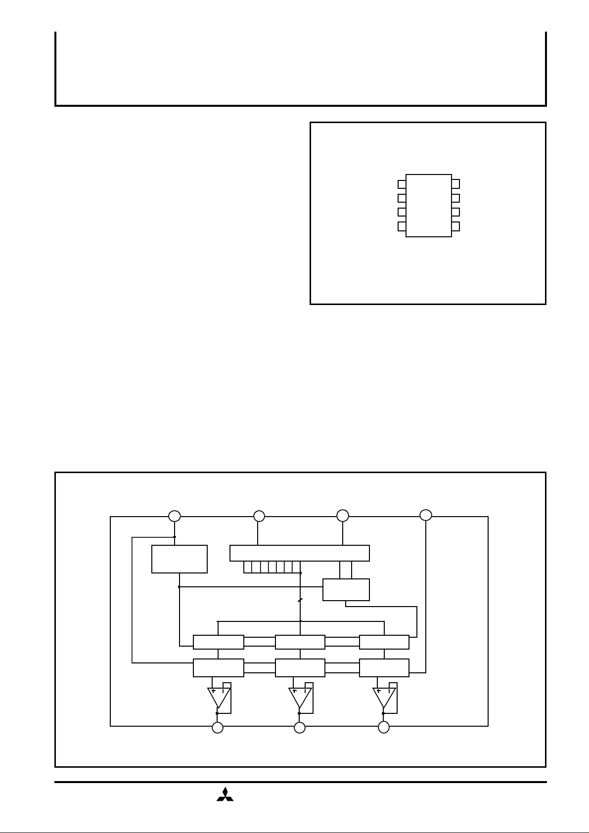
DESCRIPTION
The M62333/M62338 is an integrated circui
semiconductor of CMOS structure with 3 channels of built
in D-A converters with output buffer operational amplifiers.
The input is 2-wires serial method is used for the transfer
format of digital data to allow connection with a
microcomputer with minimum wiring.
The output buffer operational amplifier employs AB class
output circuit with sync and source drive capacity of 1.0mA
or more,and it operates in the whole voltage range from
Vcc to ground.
The M62333 and the M62338 differ only in their slave
address.
FEATURES
• Digital data transfer format
2
I
C BUS serial data method
• Output buffer operational amplifier
it operates in the whole voltage range from Vcc to
ground.
• High output current drive capacity
±1.0mA over
APPLICATION
Conversion from digital data to analog control data fo
home-use and industrial equipment.
Signal gain control or automatic adjustment of DISPLAYMONITOR or CTV.
PIN CON FIGURATION(TOP VIEW)
1
Ao1
2
Ao
Ao
3
4
Outline 8P4 (P)
M62333
M62338
8P2S-A (FP)
Vcc
8
7
6
5
N.C.:NO CONNECTION
L
NDN.C.
BLOCK DIA GRAM
Vcc
8
POWER ON
RESET
8bit Latch
8bit upper
segment R-2R
1
Ao1
SCL SDA GND
7 6 5
2
I C BUS TRANSCEIVER
CHANNEL
DECODER
8
8bit Latch
8bit upper
nt R-2R
2
Ao2
8bit Latch
8bit upper
segment R-2R
3
Ao3
MITSUBISHI ELECTRIC
980714 rev.E ( / 6 )
1
Page 2
P
MITSUBISHI <STD. LINEAR ICs>
S
P
Pin No. Symbol Function
GND
GND terminal
EXPLANATION OF TERMINALS
Vcc
VinVoPd
Topr
voltage
Buffer amplifier
output inpedance
6
7
1
2
3
8
5
SDA
SCL
Ao1
Ao2
Ao3
Vcc
Serial data input terminal
Serial clock input terminal
8-bit resolution D-A converter output terminal
Power supply terminal
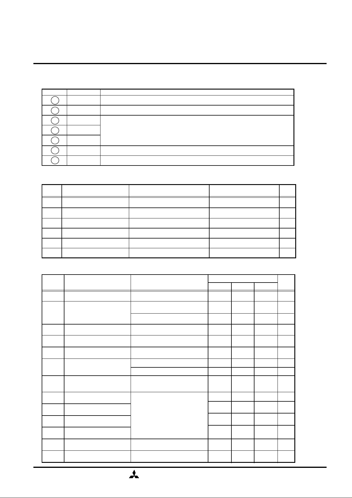
ABSOLUTE MAXIMUM RATING
M62333P/F
M62338P/F
8-BIT 3CH I2C BUS D-A CONVERTER WITH BUFFER AMPLIFIER
Symbol
Tstg
Parameter
Supply
Input voltage
Output voltage
Power dissipation
Operating temperature
Storage temperature
Conditions
Ratings
–0.3 to 7.0
–0.3 to Vcc+0.3
–0.3 to Vcc+0.3
417 (DIP) / 272 (FP)
–20 to 85
–55 to 125
Unit
V
V
V
mW
°C
°C
ELECTRICAL CHARACTERISTICS (Vcc=+5V±10%,GND=0V,Ta=–20 to 85°C unless otherwise noted)
Symbol
Icc Supply current
IILK
VIL
VIH
Buffer amplifier output
VAO
voltage range
Buffer amplifier output
IAO
drive range
SDL
Differential nonlinearity
SL
Nonlinearity
SZERO
Zero code error
Parameter Test conditions
Suplly voltage
Input leak current
Input low voltage
Input high voltage
CLK=500kHz Operation, IAO=0µA
Data : 6Ah (at maximum current )
SDA=SCL=GND,IAO=0µA
VIN=0 to Vcc
IAO=±100µA
IAO=±500µA
Upper side saturation voltage=0.3V
Lower side saturation voltage=0.2V
VCC=5.12V(20mV/LSB)
without load (IAO=0)
Ratings
MIN TYP MAX
0
0
–10 10
0.8VCC
0.1
0.2 V
–1.0
–1.0 1.0
–1.5 1.5
–2.0 2.0
0.9 2.7
0.6 1.8
0.2VCC V
VCC-0.1
VCC-0.2
1.0
Unit
VVcc 2.7 5.0 5.5
mA
mA
µA
V
V
mA
LSB
LSB
LSB
SFULL
Full scale error
Output capacitative load
Co
Ro
–2.0 2.0
MITSUBISHI ELECTRIC
5.0
0.1
LSB
µF
Ω
980714 rev.E ( / 6 )
2
Page 3

8-BIT 3CH I2C BUS D-A CONVERTER WITH BUFFER AMPLIFIER
S
0100
50
s
000ns
both S
es
300ns
0
0
0
0
units
S
S
S
S
STO
I2C BUS LINE CHARACTERISTICS
MITSUBISHI <STD. LINEAR ICs>
M62333P/FP
M62338P/FP
Symbol
fSCL
tBUF
tHD:STA
tLOW
tHIGH
tSU:STA
tHD:DAT
tSU:DAT
tR
tF
tSU:STO
SCL clock frequency
Time the bus must be free before a new transmission can start
Hold time START Condition. After this period,the first clock pulse is generated. 4.
LOW period of the clock 4.7 - µ s
HIGh period of the clock 4.
Set-up time for START condition (Only relevant for a repeated START
condition)
Hold time DATA
Set-up time DATA 2
Rise time of both SDA and SCL lines - 1
Fall time of
Set-up time for STOP condition 4.
DA and SCL lin
Parameter
Min. Max.
4.7 - µs
- µ s
- µ s
4.7 - µ s
- µ s
-n
-
-
• Note that a transmitter must internally provide at least a hold time to bridge the undefined region
(max.300 ns) of the falling edge of SCL.
KHz
µ s
TI MINGCHART
VIH
DA
VIL
tHD:STA
VIH
SCL
VIL
TART
tR, tF
tLOW tHIGH
tBUF
tHD:DATtSU:DAT
tSU:STA
TART
tSU:STO
P
TART
MITSUBISHI ELECTRIC
980714 rev.E ( / 6 )
3
Page 4

MITSUBISHI <STD. LINEAR ICs>
S
)
output
cc/256
S
cc/256
55
cc/256
cc/256
3
cc/256
cc
M62333P/FP
M62338P/FP
8-BIT 3CH I2C BUS D-A CONVERTER WITH BUFFER AMPLIFIER
I2C BUS FORMAT
STA SLAVE ADDRESS W A SUB ADDRESS A DAC DATA A STP
STA: start condition
W: write(SDA=Low
• SLAVE ADDRESS
M62333
First
1001111
• SUB ADDRESSS
First
XXX S0XXX
Don't care
• DAC DATA
First
MSB
Last
Last
S1
CHANNEL
SELECT DATA
Last
LSB
A: affirmation bit
STP: stop condition
M62338
First
1001110
CHANNEL SELECT DATA
S1
0
0
S0
0
1
01
11
Channel selection
ch1 selection
ch2 selection
ch3 selection
Don't care
Last
D2 D1 D0D3D4D5D6D7
First Last
MSBL
D7 D6 D5 D4 D3 D2 D1 D0
00000000
00000001
000000
1
00000011
::::::::
11111110
11111111
B
DAC
V
V
0
V
V
x 1
x 2
x
x 4
:
V
x 2
V
MITSUBISHI ELECTRIC
980714 rev.E ( / 6 )
4
Page 5

S
TI MING CHART(MODEL
)
SDASC
345
6
start condition to slave address bite
SDASC
345
678•sub address bite
SDASC
345
678
•
MITSUBISHI <STD. LINEAR ICs>
M62333P/FP
M62338P/FP
8-BIT 3CH I2C BUS D-A CONVERTER WITH BUFFER AMPLIFIER
L
D/A
output
start condition
12
L
D/A
output
•DAC data bite to stop condition
12 A
L
12
7W
A
A
D/A
output
With SCL at HIGH,SDA line goes from HIGH to LOW•Start condition
With SCL at HIGH,SDA line goes from LOW to HIGH •Stop condition
(Under normal circumstances,SDA is changed when SCL is LOW)
•Acknowledge bit The receiving IC has to pull down SDA line whenever receive slave data.
(The transmitting IC releases the SDA line just then transmit 8bit data.)
Digital Data Formats
STA
SLAVE ADDRESS
SUB ADDRESS 2
A
DAC DATA 2
W
A
SUB ADDRESS 1
A
A
SUB ADDRESS n
DAC DATA 1
DAC DATA n
A
stop condition
A
A
STP
MITSUBISHI ELECTRIC
980714 rev.E ( / 6 )
5
Page 6

MITSUBISHI <STD. LINEAR ICs>
S
y
CU
5
CC
3
5
M62333P/FP
M62338P/FP
8-BIT 3CH I2C BUS D-A CONVERTER WITH BUFFER AMPLIFIER
PRECAUTION FOR USE
Supply voltage terminal(Vcc) is also used for D-A converter upper reference
voltage setting. IF ripple or spike is input this terminal,accuracy of D-A conversion
is down. So,when use this device,please connect capacitor among Vcc to GND
for stable D-A conversion.
This IC's output amplifier has an advantage to capacitive load.So it's no problem
at device action when connect capacitor (0.1
ever
noise eliminate.
APPLICATION EXAMPLE
µ
F MAX) among output to GND for
V
SCL
SDA
GND
8
10µF
7
6
5
V
V
M
Analog output
terminals
1
Ao1
2
Ao2
Ao3
4
Note regarding I2C BUS
• Purchase of MITSUBISHI ELECTRIC CORPORATION'S I2C components conveys a license under the
Philips I2C Patent Rights to use these components an I2C system,provided that the system comforms to
I2C Standard Specification as defined by Philips.
Keep safety first in your circuit designs!
• Mitsubishi Electric Corporation puts the maximum effort into making semiconductor products better and
more reliable, but there is always the possibility that trouble may occur with them. Trouble with
semiconductors may lead to personal injury,fire or property damage. Remember to give due consideration
to safety when making your circuit design, in order to prevent fires from spreading, redundancy, malfunction
or other mishap.
MITSUBISHI ELECTRIC
980714 rev.E ( / 6 )
6
 Loading...