

Page 1
GENERAL DESCRIPTION
The M62320P/FP is a CMOS 8-bit I/O expander which has
serial to parallel and parallel to serial data converting
functions.
It can communicate with a microcontroller via few wiring
2
thanks to the adoption of the two-line I
C BUS.
Parallel data I/O terminal can be set to input or output
mode alternatively in individual bits.
Maximum 8 ICs can be connected to a bus by using three
chip-select pins, so that it is possible to handle up to 64 bits
data.
FEATURES
• Simple two-line (SCL and SDA) communication with a
microcontroller.
• 8-bit data conversion between serial and parallel by
2
C BUS.
I
• Built-in power-on reset.
APPLICATION
I/O port expansion for a microcontroller.
Data conversion between serial and parallel in
microcontroller peripherals.
MITSUBISHI < STD. LINEAR ICs >
M62320P,FP
16
15
14
13
12
11
10
2
CS0
CS1
CS2
V
DD
D7
D6
D5
D4
9
8-BIT I/O EXPANDER for I C BUS
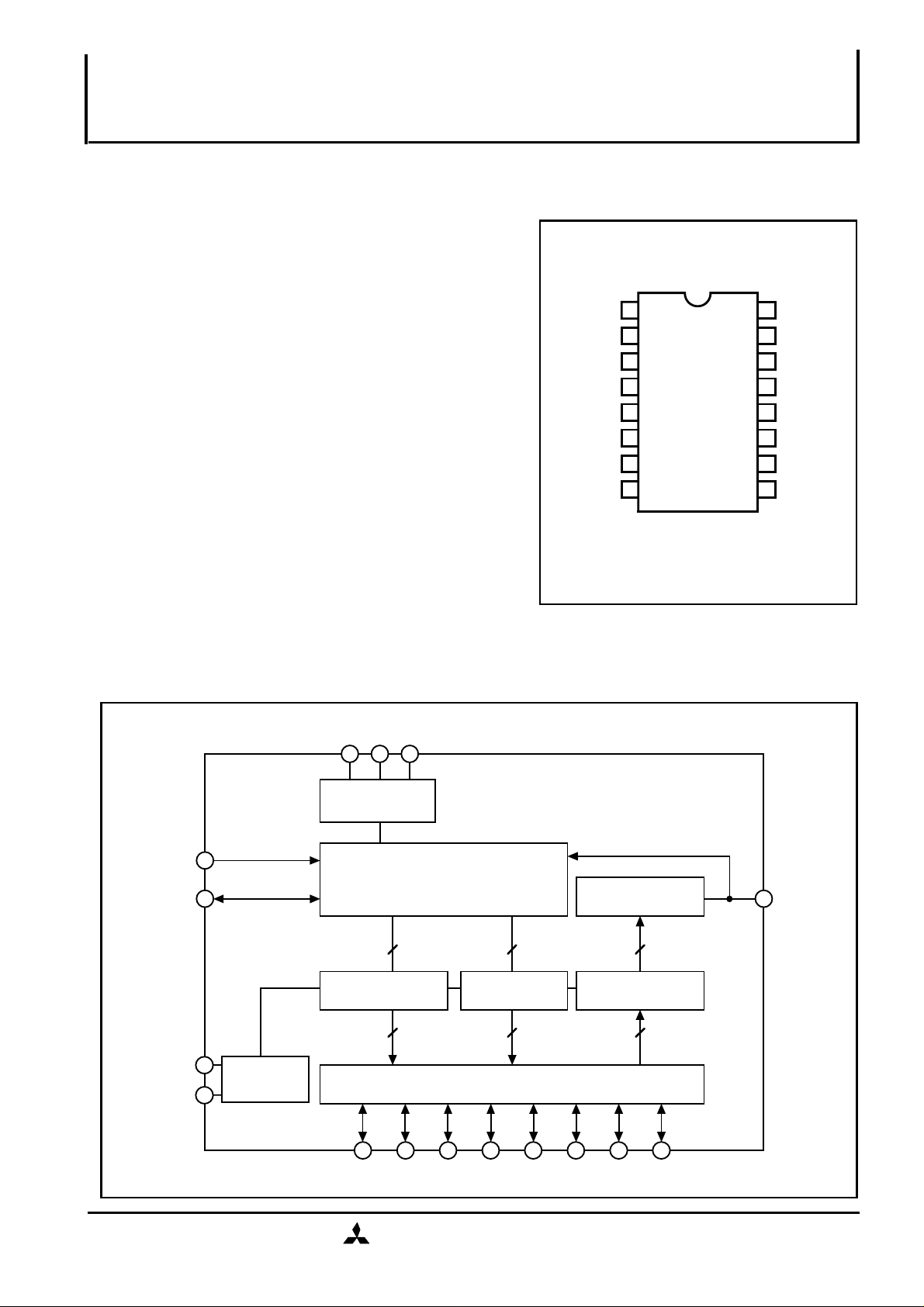
PIN CONFIGURATION(TOP VIEW)
SO
1
SCL
2
SDA
3
D0
4
D1
5
D2
6
D3
7
GND
8
Outline 16P4(P)
M62320P,FP
16P2N(FP)
BLOCK DIAGRAM
SCL
SDA
VDD
GND
2
3
13
POWER-ON
RESET
8
CS0 CS1 CS2
16
1415
CHIP-SELECT
2
I C BUS
TRANSCEIVER
Output Data
8
OUTPUT DATA
LATCH
8 8
1112
D7
I/O SETTING
DATA LATCH
Å@
I/O PORT
10
Input/Output
8
8
SHIFT
REGISTER
8
INPUT DATA
LATCH
Input Data
45679
D0D1D2D3D4D5D6
1
SO
MITSUBISHI ELECTRIC
2/20,1998(rev) ( / 9 )
1
Page 2
PIN DESCRIPTION
MITSUBISHI < STD. LINEAR ICs >
M62320P,FP
8-BIT I/O EXPANDER for I C BUS
2
16
15
14
10
11
12
13
Symbol
2
SCL Serial clock input
3
SDA
1
4
5
6
7
9
SO
CS0
CS1
CS2
D0
D1
D2
D3
D4
D5
D6
D7
V
DD
I/O
Input
Input/
Output
Output
Input
Input/
Output
Serial data input/output
Serial data output
Chip select data input
Parallel data input/output
Power supply
FunctionPin No.
GND
8
GND
MITSUBISHI ELECTRIC
2/20,1998(rev) ( / 9 )
2
Page 3
ABSOLUTE MAXIMUM RATINGS
MITSUBISHI < STD. LINEAR ICs >
M62320P,FP
8-BIT I/O EXPANDER for I C BUS
2
Symbol
VDD
VI
VO
OH
I
IOL
Pd
Supply voltage
Input voltage
Output voltage
Output current "Low"
Output current "High"
Power dissipation
Parameter
Topr Operating temperature
Tstg Storage temperature
RECOMMENDED OPERATING CONDITIONS
• Supply voltage………VDD=5V±10%
• Input high voltage……VIH=0.8VDD to VDD
• Input low voltage………VIL=0 to 0.2VDD
Conditions
D
0 to D7
D0 to D7
Ta = 25°C
Ratings
–0.3 to 7.0
–0.3 to V
–0.3 to V
DD+0.3
DD+0.3
- 5 to 0
0 to 30
1220(P) / 980(FP)
-20 to 85
-40 to 125
Unit
V
V
V
mA
mA
mW
°C
°C
ELECTRICAL CHARACTERISTICS
(VDD=5V ±10%, GND=0V,Ta=20 to 85°C, unless otherwise noted)
Symbol Parameter Conditions
VIH = VDD,VIL = GND,
f
DD
ILK Input leak current
I
VIH
V
IL
VOH
V
OL
IOL
Circuit currentI
Input high voltage
Input low voltage
Output high voltage
Output low voltage
Output current "Low"
SCL = 400kHZ
IH = VDD,VIL = GND,
V
f
SCL = stop
IOH = -1mA
I
V
V
OL = 5mA
OL = 0.4V
OL = 1.0V
Limits
Min Typ Max
0.05
0.1
-10
0.8V
DD
0.2VDD
V
DD-0.4
5
15
10
25
0.5
1.0
10
0.4
Unit
mA
µA
µA
V
V
V
V
mA
mA
MITSUBISHI ELECTRIC
2/20,1998(rev) ( / 9 )
3
Page 4

2
I C BUS CHARACTERISTICS
Symbol
fSCL
SCL clock frequency
Parameter
MITSUBISHI < STD. LINEAR ICs >
M62320P,FP
Limits
2
Max.
100
Unit
KHz
8-BIT I/O EXPANDER for I C BUS
Min.
0
tBUF
tHD:STA
tLOW
tHIGH
tSU:STA
tHD:DAT
tSU:DAT
tR
tF
tSU:STO
Free time: the bus must be free before a new transmission can start
Hold time START Condition. After this period,the first clock pulse
is generated.
LOW period of the clock
HIGh period of the clock
Set-up time for START condition (Only relevant for a repeated
START condition)
Data Hold time
Data Set-up time
Rise time of SDA and SCL signals
Fall time of SDA and SCL signals
Set-up time for STOP condition
4.7
4.0
4.7
4.0
4.7
0
250
-
-
4.0
1000
• Note that a transmitter must internally provide at least a hold time to bridge the undefined region
(max.300 ns) of the falling edge of SCL.
TIMING CHART
-
-
-
-
-
-
-
300
-
µs
µs
µs
µs
µs
µs
ns
ns
ns
µs
SDA
SCL
tR, tF
VIH
VIL
tHD:STA
tHD:DATtSU:DAT
tSU:STA
tSU:STO
VIH
VIL
tLOW
START START STOP START
tHIGH
tBUF
MITSUBISHI ELECTRIC
2/20,1998(rev) ( / 9 )
4
Page 5

MITSUBISHI < STD. LINEAR ICs >
M62320P,FP
8-BIT I/O EXPANDER for I C BUS
FUNCTIONAL BLOCKS
2
I
C BUS interface
2
The I C BUS interface recognizes start/stop conditions, a slave address and a write/read mode selection
by receiving SDA,SCL,CS0,CS1 and CS2 signals and then the latch pulses, dedicated to each data latch
are generated.
Data Latch
This IC has 3 types of data latch : the I/O setting data latch, the input data latch and the output data latch
2
and each latch is controlled by the I
• I/O setting data latch
These latches set input- or output-state of each parallel data terminals (D
byte after receiving the slave address byte in the write mode from the master. In case this latch is set to
high, the data is transferred from the I
transmission : from the parallel data terminals to the I
C BUS interface.
0 to D7). They are set at the next
2
C BUS interface to the parallel data terminals. In the opposite
2
C BUS, it is set to low.
2
• Output data latch
2
In the write mode, the data from the I
C BUS to the parallel data terminals is latched. When the master
transmits output data after a setting in write mode, the output data is taken into the latches.
• Input data latch
In the read mode, the data of parallel data terminals is latched in the input data latches. The input data is
taken into the latches from the parallel data terminals on every 8th negative edge of SCL clock . The
latched data is output to the master through the sift resistor. On the output terminal assigned by the I /
O setting latch, the input data latch takes the state of the output terminal.
Parallel input / output port
In case I/O setting latch is set to low (the input mode), each parallel terminal becomes hi-impedance and
is able to accept a input. In another case I/O setting latch is set to high (output mode), each parallel
terminal outputs a data according to the state of the output data latch.
Power on reset
When power is turned on, each latch is reset and then the parallel data I/O terminals become
hi-impedance (input mode).
MITSUBISHI ELECTRIC
2/20,1998(rev) ( / 9 )
5
Page 6

MITSUBISHI < STD. LINEAR ICs >
M62320P,FP
8-BIT I/O EXPANDER for I C BUS
DIGITAL DATA FORMAT
1. Write mode : I C BUS data input to Parallel data output
First Last
2
8BIT
DATA
2
AAAS SLAVE ADDRESS W A 8BIT DATA PI/O SETTING A 8BIT DATA
2. Read mode :Parallel data input to I C BUS data output
8BIT DATA
2
8BIT DATA
A 8BIT DATA
Transmission from Master (MCU etc.) to Slave (M62320)
Transmission from Slave (M62320) to Master (MCU etc.)
• S : Start Condition
While SCL level is high, SDA line level should be changed from high to low.
• Slave address
First
MSB
Last
LSB
0 1 1 1 A2 A1 A0
Lower three bits (A0,A1,A2) are a programmable address.
This IC is accessed only when the lower 3 bits data of slave
address coincide with the data of CS0 to CS2. (refer to the
right table)
• Chip select data
MSB LSB
A2 A1 A0
0
00L LL
00 L LH
1HLL
00
11 HH
• W: Write (SDA = LOW), R : Read (SDA = HIGH)
AAS SLAVE ADDRESS W A
CS2 CS1 CS0
1
(L=Low,H=High)
8BIT
DATA
LastFirst
P
A
H1
• A: Acknowledge bit
• I/O setting data (I/O setting of parallel data I/O terminals.)
First
MSB LSB
P3
P4P5P6P7
P2 P1 P0
DATA INPUT from parallel data terminals = Low
DATA OUTPUT to parallel data terminals = High
Last
• Each bit data corresponds to the I/O state of
the parallel data terminals.
• 8bit data
First Last
MSB
LSB
D2 D1 D0D3D4D5D6D7
• P : Stop condition
While SCL level is high, SDA level should be changed from low to high.
MITSUBISHI ELECTRIC
2/20,1998(rev) ( / 9 )
6
Page 7

MITSUBISHI < STD. LINEAR ICs >
M62320P,FP
8-BIT I/O EXPANDER for I C BUS
FUNCTIONAL DESCRIPTION
All parallel data I/O terminals are set to the input-state after power-on. In case any terminals need to be set to
the output state, the corresponding terminals should be set during the write mode. This setting is hold until a
next setting.
2
In the write mode, 8 bits data can be transmitted from the I
C BUS interface to the parallel ports continually after
the slave address and I/O setting.
2
In the read mode, 8 bits data can be transmitted from the parallel ports to the I
C BUS interface continually after
the slave address setting.
In the case of a changing between the write- and read-mode, the data must be transmitted again from the
starting condition.
• In a case of a data conversion from serial to parallel.
Transmission from a master (MCU etc.)
starting
condition
slave address I/O setting byte
DATA
Transmission from a slave (M62320)
DATA
2
stop condition
SDA
SCL
0111A2A1A00 A P7 P6 P5 P4 P3 P2 P1 P0
12345678 12345678
17D16D15D14D13D12D11D10A
A
27D26D25D24D23D22D21D20A
D
D
Data output
D0
to
D7
Hi-Z
1XD2X
D
• In a case of a data conversion from parallel to serial.
All I/O setting resistors are set to low (input) in the write mode, before a parallel data is read. (All I/O
setting resistors are set to the input mode after power-on.)
Transmission from a master (MCU etc.)
start
condition
SDA
SCL
D0 to D7
output
start
condition
slave address
0 1 1 1 A2A1A00 A P7P6P5P4P3P2P1P0
12345678 12345678
I/O setting byte
Hi-Z
slave address
DATA
A
DATA DATA
Transmission from a slave (M62320)
Data output
stop condition
SDA
SCL
D0 to D7
Input
(example)
D0 to D7
Output
011 1A2A1A01
12345
Hi-Z
D17D16D15D14D13D12D11D10A
A
67
8 12345
1XD4XD2XD3X
D
67
D37D36D35D34D33D32D31D30A
8
data latch data latch data latch
MITSUBISHI ELECTRIC
47D46D45D44D43D42D41D40A
D
2/20,1998(rev) ( / 9 )
7
Page 8

MITSUBISHI < STD. LINEAR ICs >
M62320P,FP
8-BIT I/O EXPANDER for I C BUS
• In case the I/O setting is different between each terminals.
An example : the parallel port terminals of D0 to D3 and D4 to D7 are assigned as output and input terminals,
respectively.
2
start condition
SDA
SCL
D0 to D3
D4 to D7
0 1 1 1 A2 A1 A0 0 A P7 P6 P5 P4 P3 P2 P1 P0
1234 5678 12345678
Hi-Z
Hi-Z
start condition
SDA
SCL
D0 to D3
D4 to D7
(instance)
D4 to D7
output
011 1A2A1A0 1 A
12345678 1234 5678
Hi-Z
slave address I / O setting
slave address
D17D16D15D14D13D12D11D10A
D1X
DATA
D
2X
data latch data latch data latch
DATA DATA
D
17D16D15D14D13D12D11D10
A
DATA DATA
D37D36D35D34D33D32D31D30A
3X
D
4X
D
stop condition
AD
27D26D25D24D23D22D21D20A
Data output Data output
D1XD2X
stop condition
D47D46D45D44D43D42D41D40
A
• Write mode
The terminal assigned as an output provides the data written in the output data latch.
After power-on, all terminals are reset to the input-state. Then an initial data low of the output latch are
output after the I/O setting has been done. Finally the assigned output are provided after the 8-bit data
transmission.
The terminal assigned as an input keeps the input condition (high-impedance) regardless of 8-bit data
setting.
• Read mode
The input data is taken into the input latch on every 8th negative-going edge of the SCL clock through the
terminal assigned as an input, and then the latched data is output via the SDA line.
The data of the output assigned terminal is also handled in the same procedures as above.
2/20,1998(rev) ( / 9 )
MITSUBISHI ELECTRIC
8
Page 9

TYPICAL APPLICATION
MITSUBISHI < STD. LINEAR ICs >
M62320P,FP
8-BIT I/O EXPANDER for I C BUS
2
Chip select data
MCU
10µF
14
15
16
13
VDD
4
CS2
CS1
CS0
2
SCL
3
SDA
GND
10
D0
D1
D2
D3
D4
D5
D6
D7
SO
10
11
12
5
6
7
9
1
Parallel input /
output terminal
Serial data output
PRECAUTION FOR USE
•
Purchase of MITSUBISHI ELECTRIC CORPORATION'S I C components conveys a
license under the Philips I
provided that the system conforms to I
•
Mitsubishi Electric Corporation puts the maximum effort into making semiconductor
2
C Patent Rights to use these components an I C system,
2
C Standard Specification as defined by Philips.
2
2
products better and more reliable, but there is always the possibility that trouble may occur
with them. Trouble with semiconductors may lead to personal injury,fire or property
damage. Remember to give due consideration to safety when making your circuit design,
in order to prevent fires from spreading, redundancy, malfunction or other mishap.
MITSUBISHI ELECTRIC
2/20,1998(rev) ( / 9 )
9
 Loading...