

Page 1
MITSUBISHI<Dig.Ana.INTERFACE>
prevent current leak from integration capacitor.
and speed control
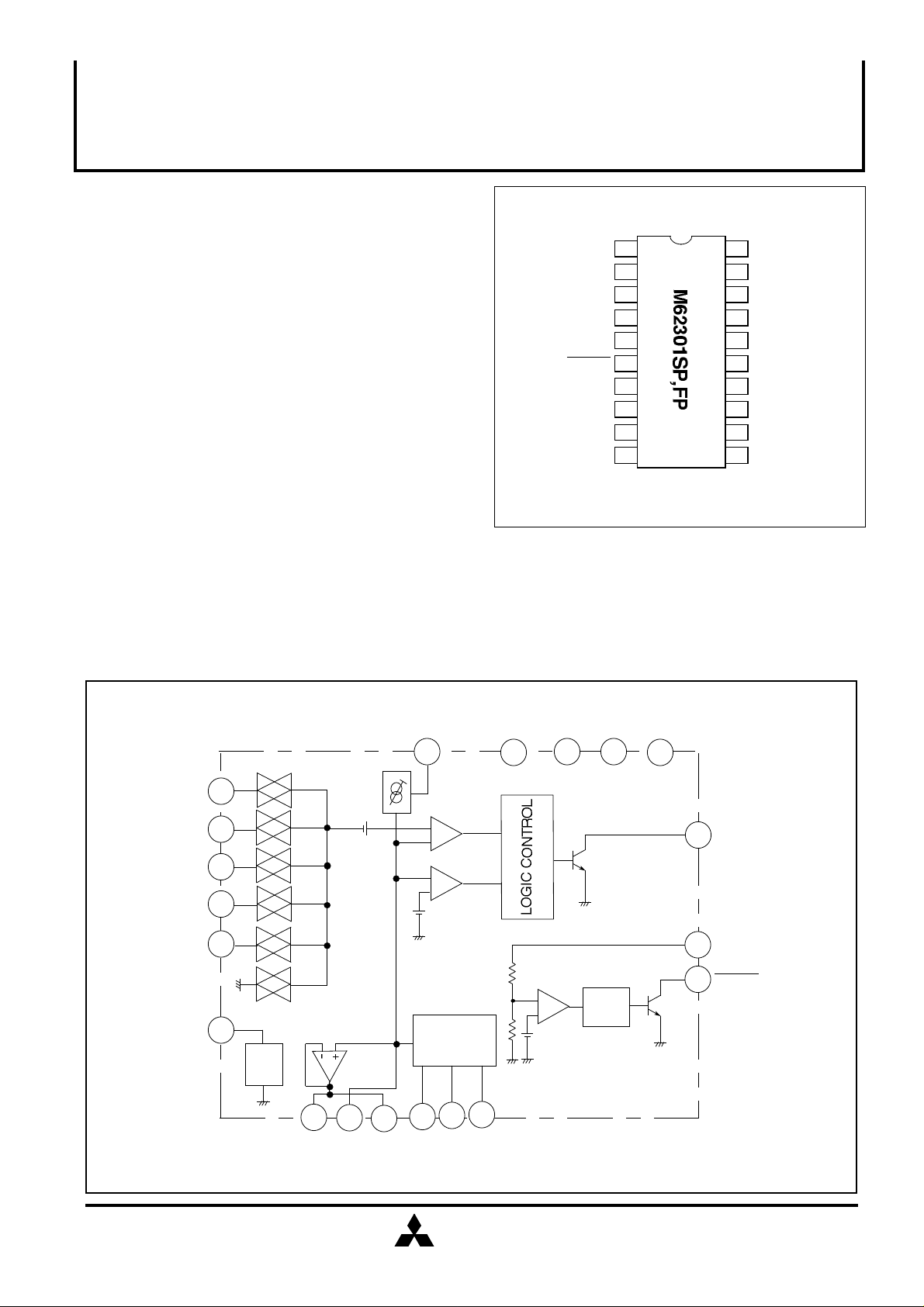
M62301SP,FP
10~12-BIT 4CH INTEGRATING A-D CONVERTER
DESCRIPTION
M62301 semiconductor integrated circuit forms an integrating
A-D converter,being connected to a microcomputer unit.By
using selection signals and counter clock signals from the
unit,a 10~12-bit A-D converter can be created at a low cost.
The integration time and resolution can be set at the user‘s
option by changing external parameters.In addition,the built-in
circuit offset,delay time and temperature fluctuation are
adjustable,enabling a wide range of applications.
M62301 has a 3 input decoder circuit,high-precision
reference voltage(1.22V)generator,current supply and
comparator for integration,and voltage-monitoring reset circuit
for a 5V power supply.It is also equipped with girdling to
FEATURES
•Separate power supplies for analog section and digital section.
•Low power dissipation.....................................2mA(typ)
(1mA for A-D conversion and the other 1mA for reset)
•Linear error......................................................±0.02%(typ)
•Conversion time...............................................526µs/ch(typ)
•Built-in system reset.........................................4.45V(typ)
APPLICATION
High-precision control systems such as temperature control
PIN CONFIGURATION (TOP VIEW)
Vcc FOR RESET
C0
C1
C2
INT
RESET
GIRDLING 1
INTEGRATING
CAPACITOR
GIRDLING 2
ANALOG GND
1
2
3
4
5
7
Outline 20P4B(SP)
20P2N-A(FP)
20
DIGITAL GND
19
A1
18
A2
17
A3
A4
16
REFERENCE INPUT
156
14
DIGITAL VDD
REFERENCE
138
VOLTAGE
CONSTANT CURRENT
129
CONTROL
1110
ANALOG Vcc
BLOCK DIAGRAM
A1
19
A2
18
A3
17
A4
16
REFERENCE
INPUT
REFERENCE
VOLTAGE
15
13
A1
A2
A3
A4
VREF
GND
VREF
1.22V
GIRDLING 1
0.49V
8
7
INTEGRATING
CAPACITOR
GIRDLING 2
CONSTANT
CURRENT
CONTROL
12
DISCHARGE
DECODER
2
9
C0
+
-
+
-
0.36V
3
C1 C2
ANALOG
Vcc
11
4
ANALOG
GND
10
+
DELAY
CIRCUIT
-
DIGITAL
GND
20
150µs
DIGITAL
VDD
14
INT
5
1
Vcc FOR RESET
RESET
6
MITSUBISHI
ELECTRIC
1
( / 9 )
Page 2
MITSUBISHI<Dig.Ana.INTERFACE>
M62301SP,FP
10~12-BIT 4CH INTEGRATING A-D CONVERTER
ABSOLUTE MAXIMUM RATINGS(Ta=25°C, unless otherwise noted)
Symbol Ratings
Vcc
VDD
VID
VIA
IoINT
IoRE
VINT
VRESET
VRE
Pd
K
Topr
Tstg
Analog section supply voltage
Digital section supply voltage
Digital input voltage
Analog input voltage
INT output current
Reset output current
INT output withstand voltage
Reset output withstand voltage
Reset supply voltage
Power dissipation
Thermal derating
Operating temperature
Storage temperature
Parameter
Conditions
-0.3~VDD+0.3
-0.3~VDD+0.3
990(DIP)/660(FP) mW
9.9(DIP)/6.6(FP)
-20 ~ +75
-55 ~ +125
15
15
15
Unit
V
8
6
6
6
V
V
V
mA
mA
V
V
V
mW/°C
°C
°C
RECOMMENDED OPERATING CONDITIONS(Ta=25°C, unless otherwise noted)
Symbol
Vcc
VDD
VIA
VIR
CI
RI
Io
Note 1.Maximum analog input voltage is less than the difference between Vcc-2.5V as well as VDD.
*Charging current II=
Analog section supply voltage
Digital section supply voltage
Analog input voltage range
(II=50µA)
Reference input voltage(II=50µA)
Integration capacity
Resistance to determine charge current
Output current
Parameter
VREF
R1
Min Typ Max
4.5
4.5
0
1
300
6
Limits
8.0
5.0
12.0
5.5
No more than(Vcc-2.5V)
and VDD(Note 1)
No more than(Vcc-2.5V)
and VDD(Note 1)
22000
60
4
Unit
V
V
V
V
pF
kΩ
mA
MITSUBISHI
ELECTRIC
2
( / 9 )
Page 3
MITSUBISHI<Dig.Ana.INTERFACE>
M62301SP,FP
10~12-BIT 4CH INTEGRATING A-D CONVERTER
ELECTRICAL CHARACTERISTICS(Vcc=5.0V,VDD=5.0V,Ta=25°C, unless otherwise noted)
75
0
30
Limits
Typ.
1.0
1.22
0.05
0.02 0.09
-0.35
0.1
4.45 4.60
150
0.1
1.0
0.75
0.6
Max.
3
50
2.0
2.5
2.2
1.27
50
-10
0.1
17
-3.5
0.8
0.4
1
80
300
0.4
1
2.0
1.0
0.8
Unit
mA
V
V
µA
%/FSR
%/FSR
µs
µs
µA
V
V
V
µA
V
mV
µs
V
µA
mA
V
Symbol
Icc
VIA
VREF
IREF +
IREF -
Ec
EL
TT
Tdi
IB
VIH
VIL
VLINT
IOHINT
VDET
∆VDET
TDE
VLRE
IOHRE
IRE
VOPL
Note 1.Conversion error;Deviation from the line that links the “0“ scale point (mode 0) and reference scale point (mode 3. VFSR=2.5V).Associated
with all channels.
Note 2.Linear error;Deviation from the line that links the 0-V input point and 2.5V input point on a given channel.
Supply current
Analog input voltage range
Reference input voltage
Permissible current inflow at
reference voltage
Conversion error
Linear error
Conversion time 526
Discharge time
Analog input current
Digital input “H“ level
Digital input “L“ level
INT output “L“ level
INT output leak current
Detection voltage
Hysteresis voltage
Delay time
Reset output “L“ level
Reset output leak current
Supply current
Limit operating voltage
Parameter
II=100µA
II=200µA
IREF=±5µA
CREF=4700pF
(Note 1)RI=24kΩ
(Note 2)RI=24kΩ
VIA=2.5V,CI=0.01µF
RI=24kΩ
V 8=3V 0.3V
CI=4700pF
IOL=1mA
V 5=15V
IOL=1mA
V 5=15V
VRE=5V
RL=2.2kΩ,VLRE≤0.4V
RL=100kΩ,VLRE≤0.4V
Test conditions
Min.
1.17
3.5
4.30
MITSUBISHI
ELECTRIC
( / 9 )
3
Page 4

10~12-BIT 4CH INTEGRATING A-D CONVERTER
12
OPERATING DESCRIPTION
(1)Decoder
Based on digital inputs to C0,C1,C2,the analog switch
is set to on,and the input of "0" scale (GND input),input
of reference scale (reference voltage input),input to
A1~A4,or discharge
MITSUBISHI<Dig.Ana.INTERFACE>
M62301SP,FP
from integration capacitor (CI) is performed.None of these operations
is performed when the "mode 8" input is given:
Mode 1 2
C0
C1
C2
Discharge
(2)A-D conversion
DECODER SELECTION MODE
VIN+0.49V
V 8
VREF+0.49V
0
0
0
0.49V
0.36V
GND
1
3 4
1
0
0
0
1
0
VREF
2
1
1
0
A1 A2
31
5 6
0
0
1
1
1
0
1
A3
4 ~ 7
7
0
1
1
A4
8
1
1
1
1
TGND TREF TIN
Multiplexer first selects VGND,obtaining minimum pulse
Note. To ensure discharge from capacitor CI,the decoder input as in
TGND.It then selects VREF,obtaining reference pulse
TREF.Input is selected next,obtaining input pulse TIN.VIN is
obtained by deducting TGND,as the offset,from TREF and
TIN.
VIN=VREF •
TIN-TG
TREF-TG
By measuring voltage at the maximum input for
approximately 500µs under the counter clock of
the above diagram should stay in mode 1 at least for the
period calculated above:
It is not necessary to measure TGND,and TREF for each
Tdi=(CI X
VIAmax+0.49
1mA
)
channel.
8MHz,resolution of approximately 12bits can be obtained;
.
500µs
=
2
125ns
.
MITSUBISHI
ELECTRIC
( / 9 )
4
Page 5

10~12-BIT 4CH INTEGRATING A-D CONVERTER
(3)Constant current control
Integrating current II can be obtained based on the reference
voltage(1.22V)by the built-in high-precision generator and
resistance RI.
1.22
II=
Integration time TI can be calculated as follows;
TI=(VIN+0.49)
(However,parameters such as built-in comparator offset
voltage,analog switch offset,voltage leak current and delay
time are not counted.)
(A)........................(1)
RI
CI
.............(2)
II
MITSUBISHI<Dig.Ana.INTERFACE>
M62301SP,FP
II
VREF
13
12
1.22V
RI
8
CI
4.45V
RESET SUPPLY VOLTAGE
VRE
0.8V
RESET OUTPUT
OUTPUT
UNSETTLED
When voltage applied to pin VRE becomes less than
4.45V,the RESET output status becomes "L".If voltage
increases over 4.50V,the RESET status becomes "H"
within 150µsec.
50mA
TDE
TDE
t
t
MITSUBISHI
ELECTRIC
5
( / 9 )
Page 6

APPLICATION SUGGESTION
11
1.4-channel 11-bit A-D converter system
MITSUBISHI<Dig.Ana.INTERFACE>
M62301SP,FP
10~12-BIT 4CH INTEGRATING A-D CONVERTER
TO MICROCOMPUTER
5V POWER SUPPLY
TO MICROCOMPUTER
CONTROL PIN
TO COUNTER
TO RESET
CI
4700pF
Charge current II =
10k 10k
CINT
680PF
50µA
1
2
3
4
1.22V
24kΩ
.
=
Resolution depends on the number of microcomputer
counter clock pulses that are generated while the INT
output status is "high" at the maximum input voltage 2.5V
(vcc-2.5V).
.
50µA
5V
20
19
18
17
165
156
147
138
129
1110
CREF
24k
RI
INPUT ANALOG
VOLTAGE
4700pF
II=50µA
CREF:To stabilize reference voltage,
be sure to connect
capacitance of approximately
4700pF.
CINT:We suggest that this capacitance
be connected to prevent
malfunction due to noise.
Use CI that leaks as slight current
as possible.To prevent leak to the
circuit board,we recommend providing
girdling 7 , 9
When the microcomputer counter clock frequency is
8MHz,the resolution can be calculated by using the
constant calculated above,as follows;
4700pFX
(2.5+0.13)
50µA
1
.
=
2
.
8M
Therefore,the resolution of this system is approximately
11 bits.
MITSUBISHI
ELECTRIC
( / 9 )
6
Page 7

10~12-BIT 4CH INTEGRATING A-D CONVERTER
12
2.4-channel 12-bit A-D converter system
Separate power supplies to analog section and digital section,
analog input voltage range mode wider up to VDD,external
reference voltage for integration.
MITSUBISHI<Dig.Ana.INTERFACE>
M62301SP,FP
TO MICROCOMPUTER
5V POWER SUPPLY
TO MICROCOMPUTER
CONTROL PIN
TO COUNTER
TO RESET
CI
6800pF
10k 10k
CINT
680pF
1
2
3
4
VDD
50µA
Because separate power supplies are provided for the
analog are digital sections,the M62301 has two supply
voltage Vcc and VDD,enabling a wide analog input voltage
range VIA.The upper limit of the range is required to be no
more than the difference between Vcc-2.5V as well as
VDD,therefore,the analog input voltage range in this
application is 0V to 5V.
A1
A2
A3
A4
8V
20
19
18
17
165
2.5V
156
147
138
129
1110
TO MICROCOMPUTER 5V POWER SUPPLY
CREF
24k
RI
INPUT ANALOG
VOLTAGE
4700pF
II=50µA
CREF:To stabilize reference voltage,
be sure to connect
capacitance of approximately
4700pF.
CINT:We suggest that this capacitance
be connected to prevent
malfunction due to noise.
Use CI that leaks as slight current
as possible.To prevent leak to the
circuit board,we recommend providing
girdling 7 , 9
When the counter clock frequency is 8MHz,resolution is:
6800pF X
(5 + 0.13)
50µA
1
.
=
2
.
8M
An A-D converter system with resolution of approximately
12 bits can be formed.
Recommended operational settings according to clock frequency,resolution,and time required for
discharge(decoder mode 1)
Counter clock Resolution
10-bit
8MHz
11-bit
12-bit
10-bit
16MHz
11-bit
12-bit
Note 1.Discharge time Tdi=(CI X
Change current
II(µA)
50
100
50
100
50
100
50
100
50
100
50
100
VIAmax+0.49
1mA
Resistance to determine
constant current RI(kΩ)
)
24
12
24
12
24
12
24
12
24
12
24
12
Integration
capacitance CI
1400pF
2800pF
2800pF
5600pF
5600pF
12000pF
700pF
1400pF
1400pF
2800pF
2800pF
5600pF
The values in this table apply when VIAmax is 5V.
MITSUBISHI
ELECTRIC
Discharge time
Tdi(µs)
7.7
15.4
15.4
30.7
30.7
65.9
3.9
7.7
7.7
15.4
15.4
30.7
7
( / 9 )
Page 8

TYPICAL CHARACTERISTICS
MITSUBISHI<Dig.Ana.INTERFACE>
M62301SP,FP
10~12-BIT 4CH INTEGRATING A-D CONVERTER
1000
800
600
400
200
1.24
1.23
1.22
THERMAL DERATING
0
0
25
50
75
AMBIENT TEMPERATURE Ta(°C)
STANDARD VOLTAGE VS.
AMBIENT TEMPERATURE
100
125
ANALOG PART SUPPLY CURRENT
VS.SUPPLY VOLTAGE
2.0
1.0
0
0
0.05
0.04
0.03
5
ANALOG Vcc (V)
LINEAR ERROR
10
1.21
1.20
1.19
-20 0
AMBIENT TEMPERATURE Ta (V)
1.0
0.9
0.8
0.7
0.6
0.5
0.4
0.3
0.2
0.1
0
0 0.1
INT OUTPUT CURRENT IO INT (mA)
20 40 60 80
INT OUTPUT “L“ LEVEL
VS.OUTPUT CURRENT
0.02
0.01
0
0
(OSR)
ANALOG INPUT RANGE VIA(V)
INT OUTPUT VS.AMBIENT TEMPERATURE
200
100
1
10
0
-20
0 20 40
AMBIENT TEMPERATURE Ta (°C)
1.0
RI=24kΩ
RI=12kΩ
2.0
60
2.5
(FSR)
80
MITSUBISHI
ELECTRIC
( / 9 )
8
Page 9

MITSUBISHI<Dig.Ana.INTERFACE>
M62301SP,FP
10~12-BIT 4CH INTEGRATING A-D CONVERTER
RESET SUPPLY CURRENT VS.
SUPPLY VOLTAGE
2.0
1.8
1.6
1.4
1.2
1.0
0.8
0.6
0.4
0.2
0
0
1.0
0.9
0.8
0.7
0.6
0.5
0.4
0.3
0.2
0.1
0
0 0.1
RESET OUTPUT CURRENT IORE (mA)
3
2
1
RESET VOLTAGE Vcc VRE (V)
RESET OUTPUT “L“ LEVEL
VS.OUTPUT CURRENT
4
5 6 7
1
DETECTION VOLTAGE vs.
AMBIENT TEMPERATURE
4.7
4.6
4.5
4.4
4.3
10
9
8
10
4.2
-20
DELAY TIME VS.AMBIENT TEMPERATURE
250
200
150
100
50
0
-20
0
20 40 60
AMBIENT TEMPERATURE Ta(°C)
0
20 40 60
AMBIENT TEMPERATURE Ta(°C)
80
80
LIMIT RESET VOLTAGE
2.0
1.8
1.6
1.4
1.2
1.0
0.8
0.6
0.4
0.2
0
0
0.6
RESET VOLTAGE Vcc VRE (V)
1.0
RL=2.2kΩ
RL=100kΩ
2.0
MITSUBISHI
ELECTRIC
( / 9 )
9
 Loading...