

Page 1
MITSUBISHI(Standard Linear ICs)
3.3V, 2.0V FIXED 2-OUTPUT VOLTAGE DC-DC CONVERTER
DESCRIPTION
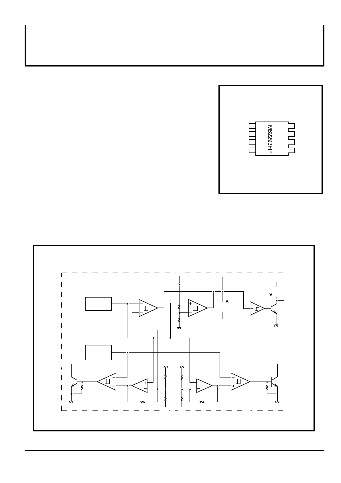
PIN CONFIGURATION
(
TOP VIEW)
Outline 8P2S-A
M62293FP is 3.3V and 2.5V fixed stable 2-output step-down DC-DC
converter.
It is possible to simplify peripheral circuit and to design compact and low
cost sets because this device includes peripheral devices in small size
8pin package.
The IC also has Reset circuit with time delay that monitors power
supply(Vcc=5V) and one regulator output(Vout1=3.3V;IN1 terminal),
therefore an application system is protected system errors.
Especially this is most suitable for application sysytem with
microprocessor and ASIC.
FEATURES
•3.3V and 2.0V step-down converter
•4 to 15V wide input supply voltage (Vcc=5V typ.)
•Reset circuit with time delay monitors
supply voltage(Vcc=5V)and regulator output (3.3V)
•110kHz fixed frequency oscillator without peripheral devices
•8pin SOP package
M62294FP
Cout1
GND
Cout2
Vcc
1
2
3
4
8
7
6
5
IN1
RESET
Cd
IN2
APPLICATION
application system with microprocessor and ASIC
BLOCK DIAGRAM
Vref
1.25V
comparator
(3.3V detect) (Vcc detect)
oscillator
(110kHz)
Cout1
Vcc Cd
IN1;3.3V
25µA
RESET
0.6µA
comparator
Vcc
Cout2
PWM comp.
op amp op amp
4
( 1 / )
IN2(2.0V)
IN1(3.3V)
PWM comp.
GND
000131
Page 2
MITSUBISHI(Standard Linear ICs)
M62294FP
3.3V, 2.0V FIXED 2-OUTPUT VOLTAGE DC-DC CONVERTER
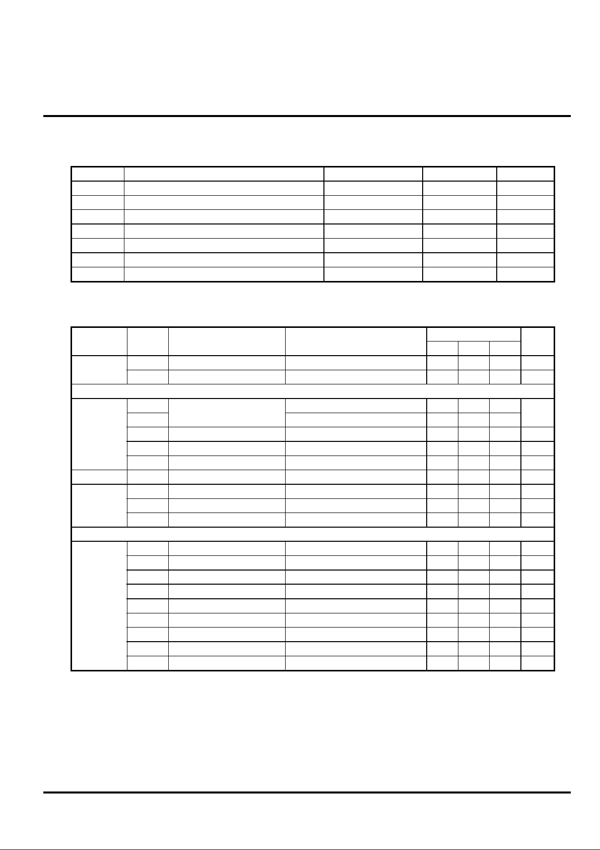
ABSOLUTE MAXIMUM RATINGS(Ta=25C,unless otherwise noted)
Symbol Parameter Conditions Ratings Unit
Vcc
Io
Pd Power dissipation
Kθ
Topr
Tstg
Supply voltage
Output current(DC-DC converter block)
Output current(Reset block)IoRESET mA
Thermal derating
Operating temperature
Storage temperature
ch1,ch2
Ta=25ºC
Ta>25ºC
ELECTRICAL CHARACTERISTICS(Ta=25C,Vcc=5V,unless otherwise noted)
16 V
30
6
440 mW
4.4
-20~+85
-40~+125
mA
mW/ºC
ºC
ºC
Block Parameter Test condition
All
Blocks
DC-DC Converter Block
Error Amp.
Oscillator
Output
Reset circuit Block
Reset
Circuit
Symbol
Vcc
Icc
Vo1
Vo2
Vreg-L
Iin
fosc
TDUTY
Vsat
Vs1
∆ Vs1
Vs2
∆ Vs2
Supply voltage
Supply current
Output voltage V
Line regulation
Input current 1
Input current 2
Oscillator frequency
Maximum ON duty
Output leakage current Vcc=12V, Vc=12VICL
Output saturation voltage Io=10mA,Darlington connection
Detecting voltage 1
hysterisys voltage 1
Detecting voltage 2
Hysterisys voltage 2
Cd output currentIPD
Delay time Cd=4700pFtpd msec
RESET output current
RESET LOW voltageVOL
RESET High voltageVOH
Without load
ch1 output
ch2 output
Vcc=4~12V
ch1
ch2
Vcc=5V detection
ch1output(3.3V)detection
Vcc=5V, Vo=1/2 X VccIOC µA-25-40 -17
IoRESET=4mA
Limits
Min. Typ. Max.
4.0 V
3.15 3.30 3.45
1.90 2.00 2.10
150 450
65 KHz
110
-1
3.6 4.0
2.46 2.70
-1.1
0.8Vo1
2.58
-0.6
5 20
15
5.0
1.5
2.8
5 15
160
90
1.2 2.0 V
3.8
5030 80
5030 80
10
1
-0.3
0.2Vo1
Unit
mA
mV
µA
µAIin 100 300
%
V
V
mV
V
mV
µA
V
V
( 2 / )
4
000131
Page 3

RESET BLOCK timing chart
3.85V
3.80V
3.3V
2.63V
td
Vo1tdtd0V0V
0V
MITSUBISHI(Standard Linear ICs)
M62294FP
3.3V, 2.0V FIXED 2-OUTPUT VOLTAGE DC-DC CONVERTER
5V
2.58V
t
t
td : RESET Delay Time ···
td(msec) = 2.13 X 10 X Cd(pF)
.
.
t
-3
( 3 / )( 3 / )4
000131
Page 4

APPLICATION CIRCUIT (3.3V and 2.0V 2-output voltage DC-DC converter
M62294FP
MITSUBISHI(Standard Linear ICs)
M62294FP
3.3V, 2.0V FIXED 2-OUTPUT VOLTAGE DC-DC CONVERTER
V IN(5V)
V OUT1(3.3V)
Co1
V OUT2(2.0V)
Co2
+
Cin
Vcc
+
IN1
IN2
+
RESET Cd
2.0V LINE
Cout1
Cout2
GND
R2
R1
3.3V LINE
L1
Q1
D1
R3
R4
L2
Q2
D2
MCU etc.
THE EXPRESSION OF CIRCUIT CONSTANTS
Constants
TON
TOFF
(TON+TOFF)MAX
TOFF(MIN)
TON(MAX)
L(MIN)
Ipk
note:
·VF : Forward voltage drop of an external diode
·Vsat : Output saturation voltage of an external switching transistor.
·∆IO : Set to 1/3 to 1/5 of maximum output current.
·Choose an external transistor, diode and inductor with peak current rating
approximately greater than "Ipk".
1
fosc
( T ON + TOFF ) /
( VIN - VCE(sat) - VO ) X TON(MAX)
Expressions
VO+VF
VIN - VCE(sat) - VO
fosc:110KHz(Vcc=5V)
(
1
- TOFF
fosc
∆Io
1
Io +
∆Io
2
1 +
TON
TOFF
)
( 4 / )
4
000131
 Loading...