

Page 1
MITSUBISHI SEMICONDUCTORS<DIGI.ANA.INTERFACE>
PRELIMINALY
PRELIMINALY
Notices;This is not a final specification.
Some parametric limits are subject to change.
GENERAL DESCRIPTION
The M62262FP is a CMOS voltage converter for driving MMICs.
It includes a input inverter utilizing a charge-pump technique, therefore
it can provide both a just inverted output (-Vo) and a twice inverted
output (-2Vo) by connecting an external capacitor.
It can also switch over between a stand-by mode (a halt function with
low power dissipation) and a double clocking mode for reducing output
ripples.
FEATURE
• Availability of two outputs ; just inverted and twice inverted output
• Capability of output current ------- 30mA (min)
• Low voltage operation ------- Vin = 3V (typ)
• Low stand-by current (standby mode)
• Low out ripple (double clocking mode)
• Small 10-pin package
APPLICATION
• MMICs for a handy telephone and a PHS
M62262FP
VOLTAGE CONVERTER FOR MMIC
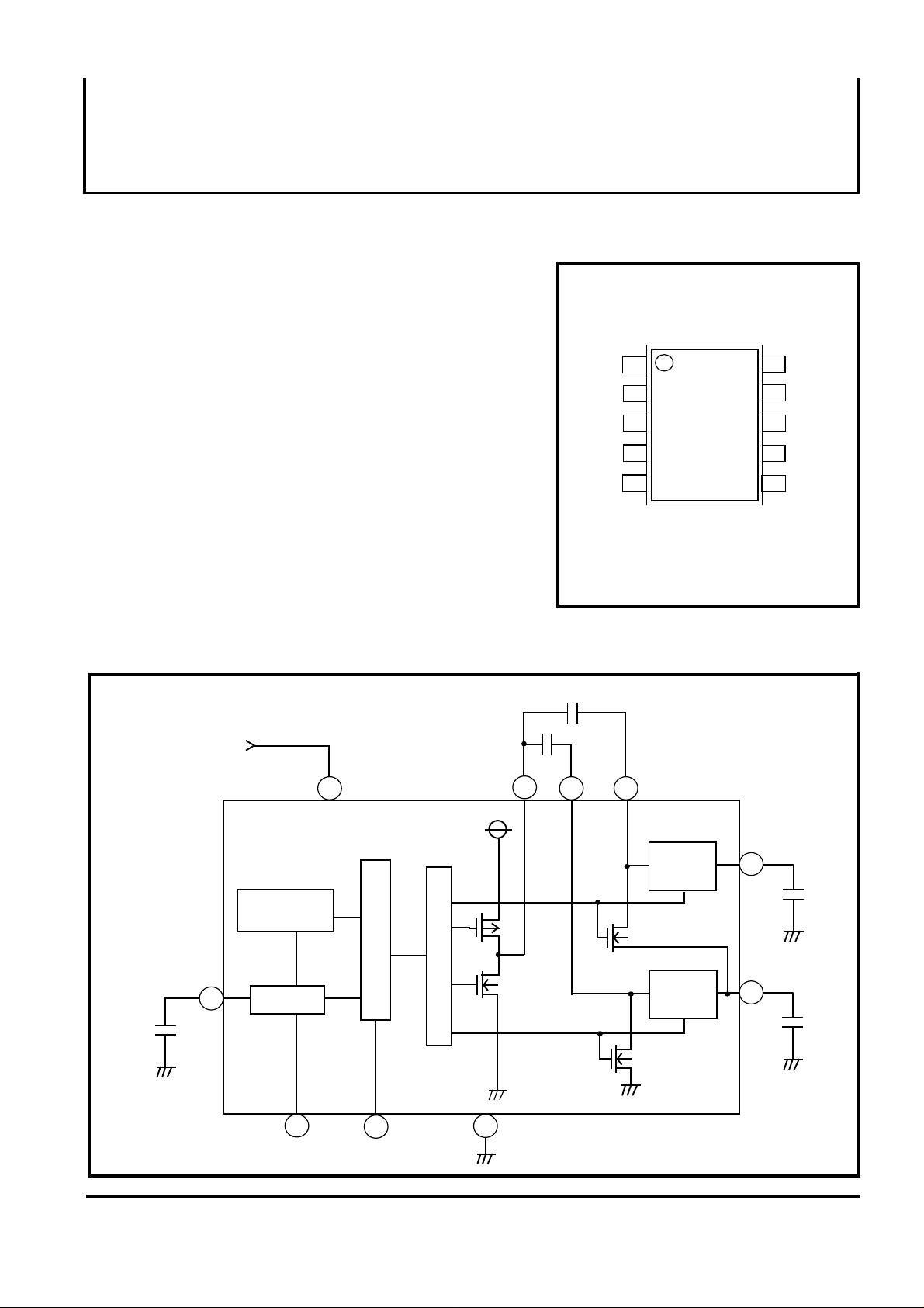
PIN CONFIGURATION(TOP VIEW)
COSC
VCC
CP1
GND
CP2
1
2
3
4
5
OUTLINE 10P2N
10 STB
9
8
-2VO
7
6
DCLK
-VO
CP3
BLOCK DIAGRAM
VCC=3V(typ)
COSC
1
VCC
Double clock
generator
Oscillator
STB
5
CP2
CP3
6
CHARGE
SW.
CHARGE
SW.
-2VO
7
-VO
8
CP1
2
Double clock selector
9
DCLK
Timing adjustment
3
410
GND
MITSUBISHI
( / 3 )
1
Page 2
MITSUBISHI SEMICONDUCTORS<DIGI.ANA.INTERFACE>
PRELIMINALY
PRELIMINALY
Notices;This is not a final specification.
Some parametric limits are subject to change.
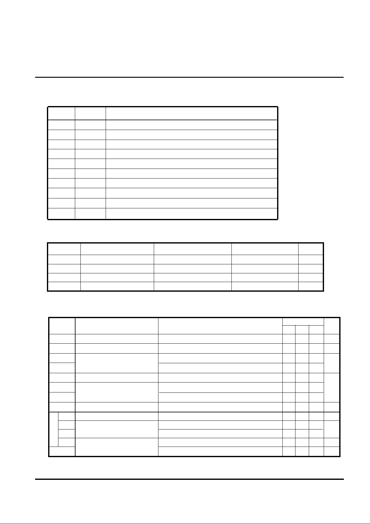
FUNCTION DESCRIPTION OF EACH PIN
PIN No. SYMBOL FUNCTION DESCRIPTION
1
2
3
4
5
6
7
8
9
COSC
VCC
CP1
GND
CP2
CP3
-2VO
-VO
DCLK
STB10
Connecting pin for capacitance of oscillator
Input voltage
Connecting pin 1 for a capacitor of charge-pump
GND pin
Connecting pin 2 for a capacitor of charge-pump
Connecting pin 3 for a capacitor of charge-pump
2-times inverted output
Just inverted output
Switchover between double cloking (H) and normal mode (L)
Switchover between stand-by (H) and actual operation (L)
ABSOLUTE MAXIMUM RATINGS(Ta=25°C unless otherwise noted)
M62262FP
VOLTAGE CONVERTER FOR MMIC
SYMBOL
VCC
PD
To p r
Ts t g
ELECTRICAL CHARACTERISTICS
SYMBOL
ICC
VCC
RO1
RO2
VEF
PEF2
fOSC COSC=220PF
DCLK
ISTB STB=VCC 2
Voltage conversion efficiency
ICC
RO1
RO2
fOSC
PARAMETER CONDITIONS
Supply voltage
Internal power dissipation
Operating temperture
Storage temperture
(VIN =3V, COSC=220PF, Ta=25°C, unless otherwise noted )
PARAMETER
Dissipation current
Range of sourse voltage
Output resistor
Power efficiency
Oscillating frequency
Dissipation current
Output resistor
Standby current
-Vout output pin (with load at -Vout pin only)
-2Vout output pin(with load at -2Vout pin only)
No load
-Vout output pin , IL=-5mA
-2Vout output pin , IL=-5mA
DCLK=VCC
-Vout output pin (with load at -Vout pin only)
-2Vout output pin(with load at -2Vout pin only)
COSC=220PF
CONDITIONS
RATINGS
6 V
440
- 20 ~ + 75
- 40 ~ +125
RATINGS
MIN TYP
450 900
30 60
90
99.8
95
90
90
6
2
0.6
20 40
60 120
12 20 kHz
4
UNIT
mW
°C
°C
MAX
180
5.52.7
10
UNIT
µA
V
Ω
%PEF1
kHz
mA
1
Ω
µA
5
MITSUBISHI
( / 3 )
2
Page 3

MITSUBISHI SEMICONDUCTORS<DIGI.ANA.INTERFACE>
PRELIMINALY
PRELIMINALY
Notices;This is not a final specification.
Some parametric limits are subject to change.
AN EXAMPLE APPLICATION CIRCUIT
10µF
+
6
VCC
2
3V
COSC
1
220pF
M62262FP
4
GND
10µF
+
3
DCLK 10
9
M62262FP
VOLTAGE CONVERTER FOR MMIC
5
CP2CP1CP3
-VO
-3V
STB
8
-2VO
7
10µF
+
10µF
+
-6V
Mitsubishi Electric Corporation puts the maximum effort into making semiconductor products better and more reliable,but
!
there is always the possibility that trouble may occur with them.Trouble with semiconductors may lead to personal injury,
fire or property damage.Remember to give due consideration to safety when making your circuit design,in order to
prevent fires from spreading,redundancy,malfunction or other mishap.
MITSUBISHI
( / 3 )
3
 Loading...