

Page 1
DESCRIPTION
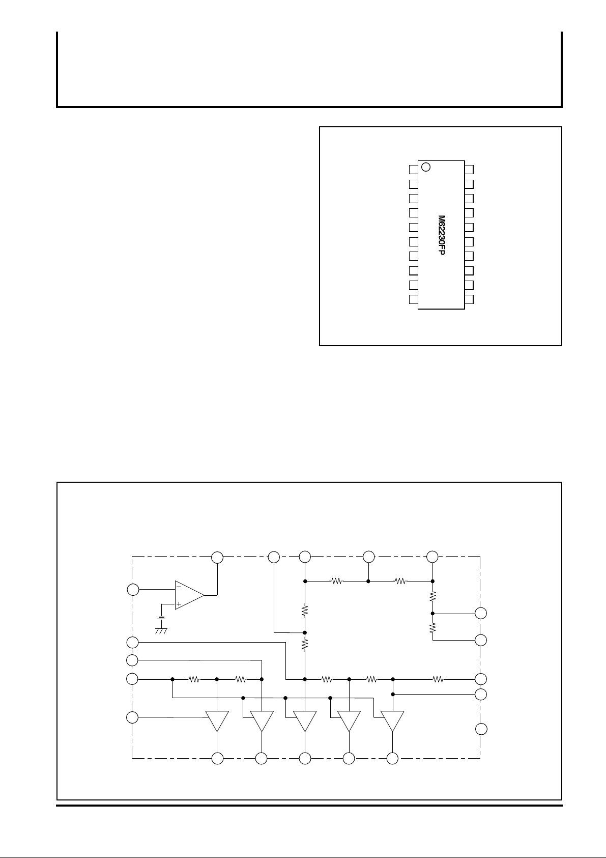
PIN CONFIGURATION (TOP VIEW)
The M62230FP is a semiconductor circuit for LCD matrix regulator,
which will generate the diveded-voltage to drive LCD matrix.
By changing the connection of R pin(i.e.,Change the internal
resistor ratio), M62230FP can support divided voltage ratio ranging
from 1/5 bias to 1/13 bias.
The high stability and any desired voltage levels is possible, since
the variable voltage regulator for Vref is built-in.
FEATURES
•Adjustable type voltage divider.
(The setting range of internal resistor is from 1/5 bias to 1/13
bias)
•5 resident buffer-Amp. (5 divided output)
•Low power dissipation(1.8 mA Typ.)
•Resident voltage-variable regulator for Vref.
MITSUBISHI (Dig./Ana. INTERFACE)
M62230FP
LCD MATRIX REGULATOR
R6
R5
R4
R3
R2
R1
REGOUT
REGIN
VIN3
VIN2
1
2
3
4
5
6
7
8
9
10
Outline 20P2N-A
VREF
20
VIN5
19
VCC
18
VO5
17
VO4
16
VO3
15
VO2
14
VO1
13
12
GND
11
VIN
APPLICATION
To drive LCD.
RECOMMEND OPERATING CONDITIONS (Ta=25°C)
Supply voltage range : GND-Vcc :(if V 1 > -1V, it is necessary to
support V IN)........ -30 to -10V
Recommend input voltage GND-VREF :VREF ≥ Vcc........ -30 to -6V
(To set Vcc, VREF, in order that both I 0-V2 I & I VCC-V5 I
are larger than 1V)
BLOCK DIAGRAM
R1 R2 R3 R4
6
REGIN
VIN3
VIN2
GND
REGOUT
7
8
-1.38V
9
10
12
R R
R R
R
4R
R R
45
3
R
2
R5
R
1
R6
20
R
VREF
19
VIN5
11
VIN
13 14 15 16
VO1 VO2 VO3 VO4 VO5
( / 4 )
1
17
18
VCC
Page 2
EXPLANATION OF TERMINALS
Pin No.
1
2
3
4
5
6
7
8
9
10
11
12
13
14
15
16
17
18
19
20
Symbol
R6
R5
R4
R3
R2
R1
REGOUT
REGIN
VIN3
VIN2
VIN
GND
VO1
VO2
VO3
VO4
VO5
VCC
VIN5
VREF
If the voltage of each pin can satisfy the following condition:
these pins will be used.
Please refer to page. 4 to set the bias ratio.
Regulator output for VREF to use
The inverting input pin of REG OP-Amp
VIN3 Input
VIN2 Input
VIN Power
GND Pin
Divided-voltage output pin
To set VCC & VREF, in order that 0 - V2 ≥ 1V
To set VCC & VREF, in order that V5 - VCC ≥ 1V
VCC Power (-Power)
VIN5 input
Reference voltage input pin
MITSUBISHI (Dig./Ana. INTERFACE)
M62230FP
LCD MATRIX REGULATOR
Function
VO6 ≥ VO5 ≥ VO4 ≥ VO3 ≥ VO2 ≥ VO1
if V1 > -1.0V, it is necessary to support VIN
if V1 < -1.0V, this pin connect to GND
( / 4 )
2
Page 3

MITSUBISHI (Dig./Ana. INTERFACE)
M62230FP
LCD MATRIX REGULATOR
ABSOLUTE MAXIMUM RATINGS (Ta=25˚C, unless otherwise noted)
Symbol
VCC
IOUT
Pd
K
Topr
Tstg
Supply voltage
Maximum output current
Power dissipation
Thermal derating
Operating temperature
Storage temperature
Parameter Ratings
ELECTRICAL CHARACTERISTICS(Vcc=-16V, VIN=GND, VREF=-12V, Resistor setting=5R, Ta=25°C, unless otherwise noted)
Parameter Test conditionsSymbol
VCC
ICC
RVO1
RVO2
RVO3
RVO4
RVO5
RR1
RR2
RR3
RR4
RR5
RR6
R
∆V1
∆V2-1
∆V3-1
∆V2-2
∆V3-2
∆V4
∆V5
VREG
REG-L
Supply voltage
Dissipation current
Output voltage ratio 1
Output voltage ratio 2
Output voltage ratio 3
Output voltage ratio 4
Output voltage ratio 5
Output voltage ratio 6RVO6 V5/(V5-V4)
Resistor ratio 1
Resistor ratio 2
Resistor ratio 3
Resistor ratio 4
Resistor ratio 5
Resistor ratio 6
Resistance
Load regulation of output voltage 1
Load regulation of output voltage 2-1
Load regulation of output voltage 3-1
Load regulation of output voltage 2-2
Load regulation of output voltage 3-2
Load regulation of output voltage 4
Load regulation of output voltage 5
Output voltage of regulator
Load regulation of VREF
VREF= -16V
V2/V1
(V5-V3)/(V5-V4)
V5/V1
V5/V2
V5/(V5-V3)
Resistor between VIN3 and R1/ resistor
between R1 and R2
Resistor between VIN3 and R2/ resistor
between R1 and R2
Resistor between VIN3 and R3/ resistor
between R1 and R2
Resistor between VIN3 and R4/ resistor
between R1 and R2
Resistor between VIN3 and R5/ resistor
between R1 and R2
Resistor between VIN3 and R6/ resistor
between R1 and R2
Resistor between R1 and R2
+200µA<IOUT1<+10mA
+200µA<IOUT2<+10mA
+200µA<IOUT3<+10mA
-10mA<IOUT2<-200µA
-10mA<IOUT3<-200µA
-20mA<IOUT4<-200µA
-20mA<IOUT5<-200µA
Buffer output
-10mA<IREG<+2mA
Conditions
Ta=25°C
Ta>25°C
-36 to 0
550
5.5
-20 to +75
-40 to +125
Limits
Typ. Max.Min.
-35
1.80
1.98 2.00
1.98
8.90
4.45
4.45
8.90
-1.45
2.00
9.00
4.50
4.50
9.00
-1.38
30
mW/°C
Unit
-10
2.02
2.02
9.10
4.55
4.55
9.10
4
5
6
7
8
9
20
20
20
20
20
20
20
20
-1.31
50
Unit
V
mA
mW
°C
°C
V
mA
kΩ
mV
mV
mV
mV
mV
mV
mV
V
mV
( / 4 )
3
Page 4

THE SETTING METHOD OF DIVIDED-VOLTAGE
R
RX
R
R
R
R
VREF
+
-
+
-
+
-
+
-
+
-
VO1
VO2
VO3
VO4
VO5
RX Bias ratio Example of setting
R
2R
3R
4R
5R
6R
7R
8R
9R
1/5
1/6
1/7
1/8
1/9
1/10
1/11
1/12
1/13
MITSUBISHI (Dig./Ana. INTERFACE)
M62230FP
LCD MATRIX REGULATOR
9 pin- 6 pin short, 10 pin- 5 pin short
9 pin- 6 pin short, 10 pin- 4 pin short
9 pin- 6 pin short, 10 pin- 3 pin short
10 pin- 6 pin short
10 pin- 5 pin short
10 pin- 4 pin short
10 pin- 3 pin short
10 pin- 2 pin short
10 pin- 1 pin short
( / 4 )
4
 Loading...