

Page 1
3.0V FIXED OUTPUT VOLTAGE DC-DC CONVERTER
GENERAL DESCRIPTION
The M62221 is a general purpose DC-DC converter which
provides a 3.0V fixed output voltage.
It is possible to simplify the peripheral circuit and to design compact
and low cost sets because this IC, housed in a small 5- or 8-pin package
includes necessary peripheral components.
Especially this is most suitable for CD-ROM, Disk Drive sets and
PDA as a converter from 5V to 3.0V .
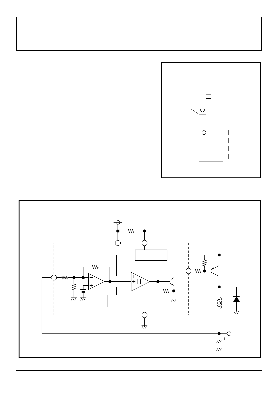
MITSUBISHI <Dig./Ana. INTERFACE>
M62221L/FP
PIN CONFIGURATION (TOP VIEW)
5
IN
4
VCC
3
CLM
2
GND
M62221L
1
COLLECTOR
FEATURES
• Wide operation supply voltage range ·········· 4 to 15 V
• Low power consumption ·········· 900 µA(max.)
• Built-in oscillator without external components (110kHz typ.)
• Built-in over current protection circuit
• Small size 5-pin SIP and 8-pin SOP packages
APPLICATIONS
CD-ROM, PDA, general purpose electric products
BLOCK DIAGRAM
OVER CURRENT
VCC
OP Amp
DETECTION RESISTOR
CURRENT LIMIT
CIRCUIT
34
CLM
COLLECTOR
GND
CLM
VCC IN
Outline 5P5T
1
2
3
4
Outline 8P2S-A
M62221FP
8
7
6
5
NC: NO CONNECTION
NC
NC
NC
IN
PWM Comp
5
1.25V
OSC
(110KHz)
2
GND
1
Collector
OUT
( 1 / 3 )
April. 1997
Page 2
MITSUBISHI <Dig./Ana. INTERFACE>
M62221L/FP
3.0V FIXED OUTPUT VOLTAGE DC-DC CONVERTER
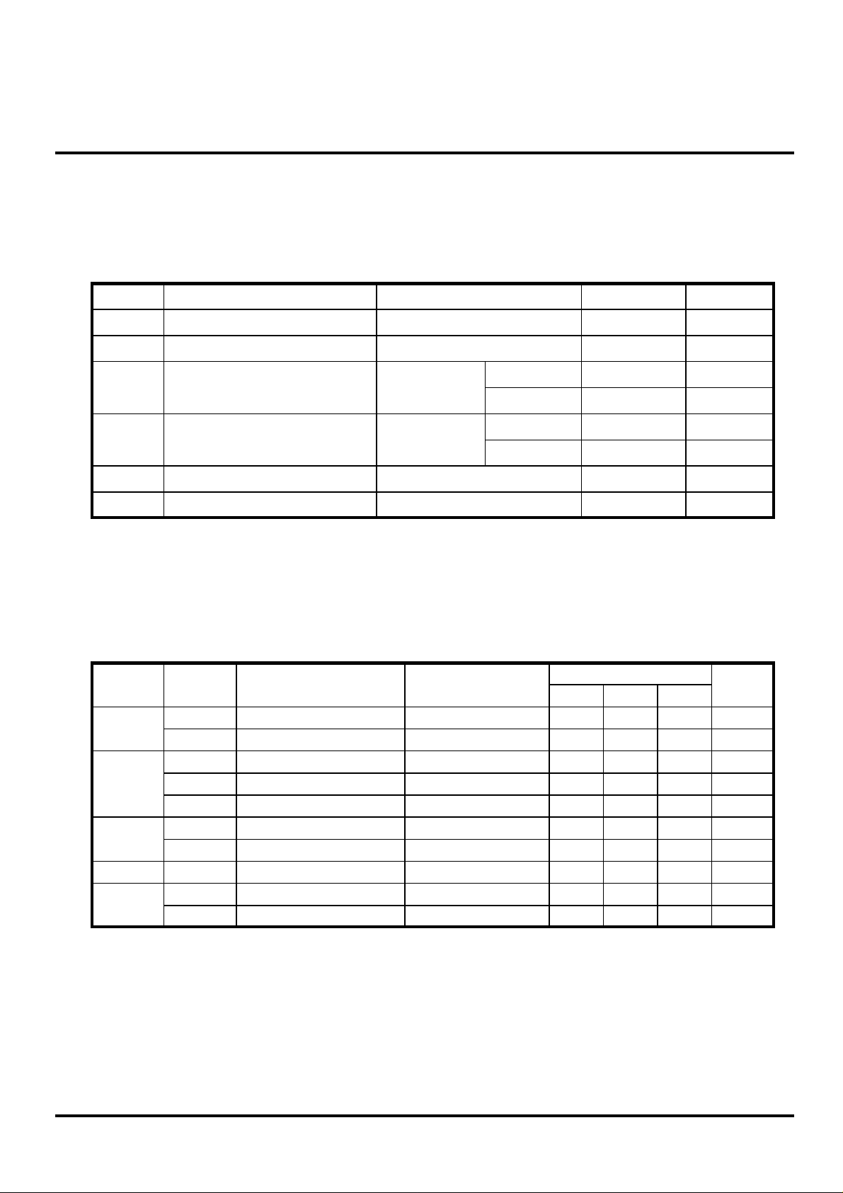
ABSOLUTE MAXIMUM RATINGS (Ta=25°C, unless otherwise noted)
Symbol Parameter Conditions Ratings Unit
Vcc
Io
Pd Power dissipation
KTHETA
Topr
Tstg
Supply voltage
Output current
Thermal derating
Operating ambient temperature
Storage temperature
Ta=25°C
Ta>25°C
5-pin SIP
8-pin SOP
5-pin SIP
8-pin SOP
16
100 mA
450 mW
4.5
4.4
-20 to +85
-40 to +125
ELECTRICAL CHARACTERISTICS (Ta=25°C, Vcc=5V, unless otherwise noted)
Block Symbol
All
block
Error
Amp.
Oscillator
CLM
Output
Vcc Supply voltage
Icc
Vreg-L
Iin
fosc
TDUTY
VTHCLM
ICL
Vsat
Vo
Parameter
Supply current
Output voltage
REF line regulation
IN input current
Oscillator frequency 110
Maximum on duty
Current limit voltage 150 mV
Output leakage current
Output saturation voltage
Test conditions
Vcc= 4 to 12V
Vcc - CLM
Vcc = 12V, Vc = 12V
Io = 100mA
Min. Typ. Max.
4.0
—
—
65
120 180
-1 1
—
Limits
15
660
3.002.85 3.15
5
100
90 %
900Without load
15
300
155
—
0.4 0.7
V
mW440
mW/ °C
mW/ °C
°C
°C
Unit
V
µA
V
mV
µA
kHz
µA
V
( 2 / 3 )
April. 1997
Page 3

MITSUBISHI <Dig./Ana. INTERFACE>
3.0V FIXED OUTPUT VOLTAGE DC-DC CONVERTER
Application Circuit (3.0V Output DC-DC Converter)
RCLM
VIN (5V)
+
100µF
0.1Ω
4
3
Vcc CLM
VOUT(3.0V,1A)
100µF
IN
5
+
M62221
Collector
1
GND
M62221L/FP
1KΩ
1KΩ
2
Fig.1 Example of the M62221L/FP application circuit
• Current Limit Detection:
When the voltage drop between pin 3 and pin 4 becomes more than 150mV,
the Current Limit Detection circuit begins operating. The peak switch
current "Ipk" is limited to 150mV / RCLM. In the example of application
(fig.1), the current is limited to 1.5A.
THE EXPRESSION OF CIRCUIT CONSTANTS
CONSTANTS
TON
TOFF
(TON+TOFF)MAX
TOFF(MIN)
TON(MAX)
L(MIN)
Ipk
RCLM
( TON + TOFF ) /
( VIN - VCE(sat) - VO ) x TON(MAX)
EXPRESSIONS
VO+VF
VIN - VCE(sat) - VO
1
fosc
0.15
fosc:110KHz(Vcc=5V)
1
fosc
Io +
∆VCLM:150mV(Vcc=5V)
Ipk
- TOFF
∆Io
1
2
TON
( )
1 +
TOFF
∆Io
68µH
•VF :Forward voltage drop of an external diode.
•Vsat :Output saturation voltage of an external switching transistor.
•∆IO :It should be set between 1/3 and 1/5 of maximum output current.
•An external transistor, diode and inductor should have a peak current capability of
greater than "Ipk".
( 3 / 3 )
April. 1997
 Loading...