

Page 1
MITSUBISHI SEMICONDUCTOR < STANDARD LINEAR IC >
GENERAL PURPOSE HIGH SPEED PWM CONTROL IC
GENERAL PURPOSE HIGH SPEED PWM CONTROL IC
DESCRIPTION
M62213P/FP is designed as a general purpose high-speed
PWM control IC.
This small 10 pin package contains many function and
protection circuits allowing simpler peripheral circuits and
compact set design.
This IC can operate high speed switching (700kHz Max)
with high speed PWM comparator and current limiting circuit.
FEATURES
• 700kHz operation to MOS- FET
• Output current Io= ±1A
• Totem pole output
• Timer type latch protection circuit with OVP
• Soft start operation is possible (with dead time control)
• Built-in OPAmp for feedback control
(photo coupler can be driven)
• High speed pulse-by-pulse current limiting
• Small size 10-pin SOP package
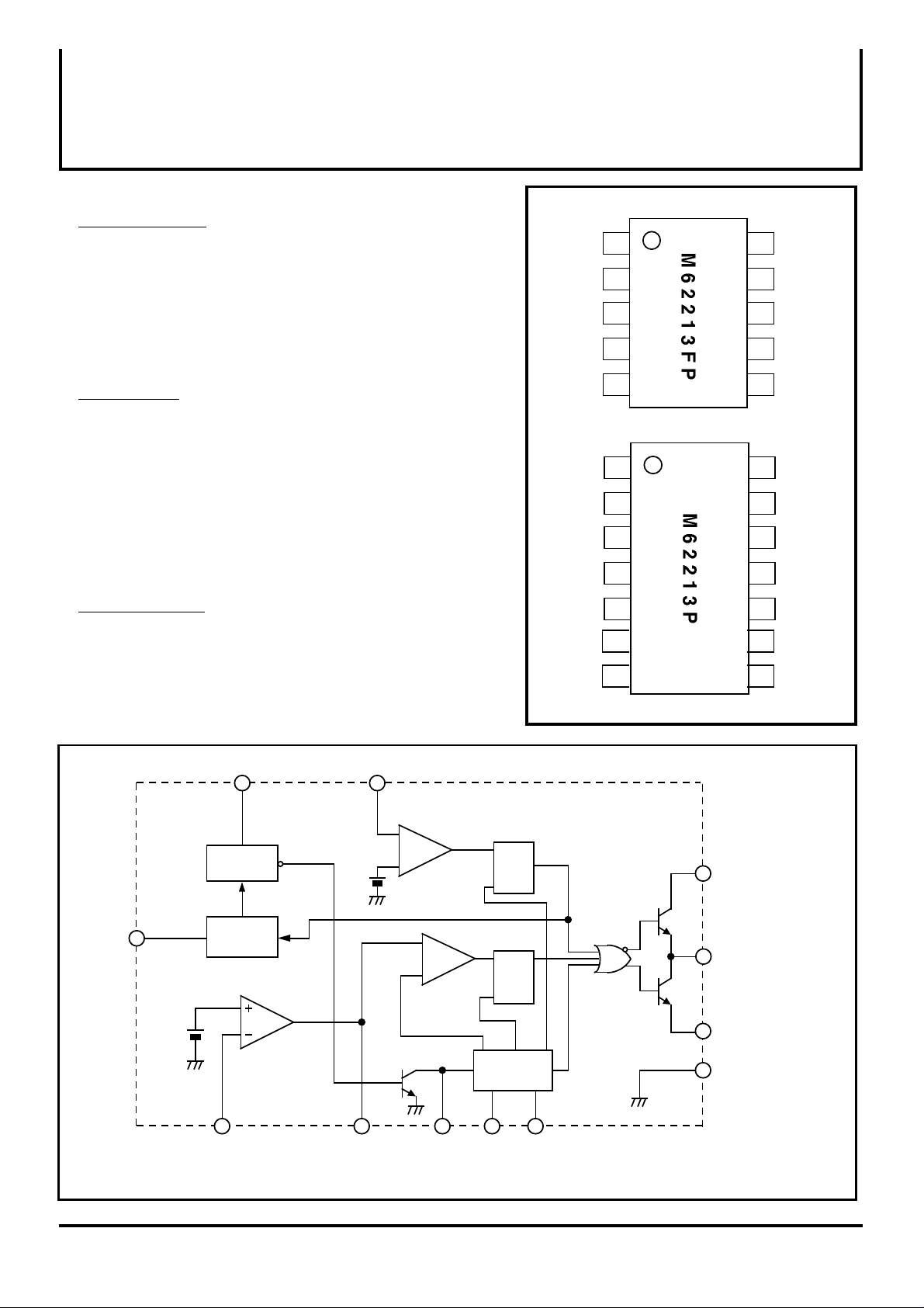
M62213P/FP
PIN CONFIGURATION (TOP VIEW)
RF
CF
1
2
3
4
5
OUTLINE 10P2N-A
1
2
3
4
VOUT
GND
CLM
VOUT
EMIT
GND
CLM
M62213P/FP
VCC
10
9
EA IN
8
EA OUT
7
SOFT
CT
6
COLLECT
14
VCC
13
12
EA IN
EA OUT
11
APPLICATION
• Switching Regulator
• DC-DC Converter
CT
(OVP)
2.5V
VCC CLM
UVLO
TIMER
LATCH
CLM
COMP
0.2V
PWM
COMP
S
CLM
LATCH
R
S
PWM
LATCH
R
RF
CF
N.C
5
6
7
OUTLINE 14P4
10
9
8
:note
COLLECT
VOUT
:note
EMIT
CT
SOFT
N.C
EA IN
EA OUT
(DTC)
( / 9 )
1
OSC.
GND
note: GND terminal is connected to emitter terminal
CFRFSOFT
as M6213FP in IC inside.
And Vcc terminal is connected to collector
terminal as M6213FP in IC inside.
Page 2
MITSUBISHI SEMICONDUCTOR < STANDARD LINEAR IC >
M62213P/FP
GENERAL PURPOSE HIGH SPEED PWM CONTROL IC
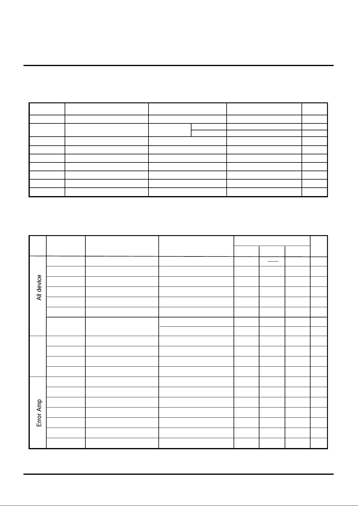
ABSOLUTE MAXIMUM RATINGS (Ta=25°C, unless otherwise noted)
Symbol Parameter Condition Rating Unit
Vcc
IOUT
VCT
VEA IN
VCLM
Pd
Ktheta
Topr
Tstg
Supply voltage
Out terminal current
CT terminal supply voltage
EA IN terminal supply voltage
CLM terminal supply voltage
Power dissipation
Thermal derating
Operating temperature
Storage temperature
Continuous
Peak
Ta=25°C
Ta≥25°C
36
150
1.0
36
10
-0.3 ~ +4.0
440
3.52
-20 ~ +85
-40 ~ +150
V
mA
A
V
V
V
mW
mW/°C
°C
°C
ELECTRICAL CHARACTERISTICS (Ta=25°C, Vcc=14V, unless otherwise noted)
Limits
Block
CT
Symbol Parameter
Vcc
Vcc(START)
Vcc(STOP)
∆Vcc
IccL
Icco
IccOFF Timer latch circuit current
VTHCTH
VTHCTL
ICTDCHG
ICTCHG
VB
IB
AV
fT
IOS
Supply voltage range
Operation start-up voltage
Operation stop voltage
Start-up and stop
voltage difference
Stand-by current
Operating current
CT term. "H" threshold voltage
CT term. "L" threshold voltage
CT term. discherge current
CT term. cherge current
Reference voltage
Input bias current
Open loop gain
Unity gain bandwidth
Output source current
Test condition
Vcc=14V
Vcc=Vcc(STOP) + 0.2V
In normal operation
In CLM actuating
When VEAIN=0V
Typ Max
Vcc
(STOP)
Min
4.23.5
90
7.5
3.5 4.5
0.4
70
-33
180
13
4.0
0.7
100
-15
2.52.4 2.6
-300
-100
70
1
-100 -60-140
13.512.511.5
9.08.37.6
5.1
270
22
1.0
130
35
-5
Unit
V
V
V
V
µA
mA
mA0.9 2.0 3.00.9
mA1.8 2.70.8
V
V
µA
µA
V
0
nA
dB
MHz
µA
VOm + Output voltage (High)
VOm - Output voltage (Low)
( / 9 )
2
4.7 5.25 6.25
0 0.1 0.3
VV
V
Page 3
MITSUBISHI SEMICONDUCTOR < STANDARD LINEAR IC >
M62213P/FP
GENERAL PURPOSE HIGH SPEED PWM CONTROL IC
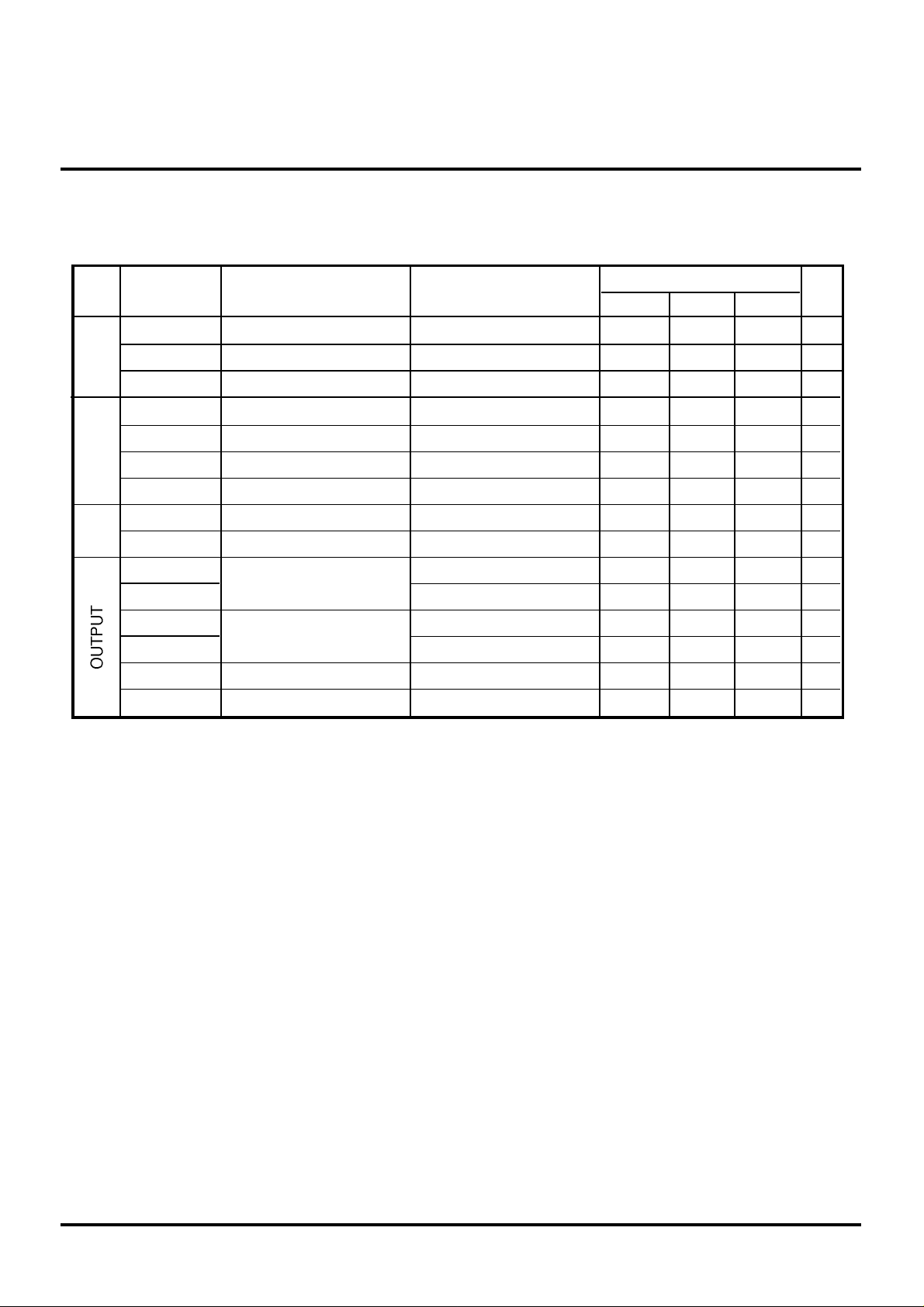
ELECTRICAL CHARACTERISTICS (Ta=25°C, Vcc=14V, unless otherwise noted)
Block
C
L
M
S
O
F
T
OSC.
Symbol
VTHCLM
IOUTCLM
TPDCLM
VSOFT(0%)
VSOFT(50%)
Duty Max
ISOFT
fOSCmax
fOSC
VOL1
VOL2
VOH1
VOH2
TRISE
TFALL
Parameter
CLM term. threshold voltage
CLM term. output current
CLM term. delay time
Input voltage range at 0% duty
Input. voltage at 50% duty
Maximum duty
Soft term. input current
Maximum oscillation frequency
Oscillation frequency
Output low voltage
Output high voltage
Output voltage rise time
Output voltage fall time
Test condition
VCLM=0V
Delay time to output
Soft term. voltage range
to set 0% duty
Soft term. voltage at 50% duty
CF=270pF , RF=69 kΩ
Vcc=14V,Io=10mA
Vcc=14V,Io=100mA
Vcc=14V,Io=-10mA
Vcc=14V,Io=-100mA
No load
No load
Limits
Min
180
-270 -140
0 0.5
80
-65 -31
150 250
Typ Max
200
220
-200
90
2.7
90
99
-50
700
200
0.04 0.4
1.40.3
12.712.0
12.511.5
50
35
Unit
V
µA
nS
V
V
%
µA
KHz
KHz
V
V
V
V
nS
nS
( / 9 )
3
Page 4

MITSUBISHI SEMICONDUCTOR < STANDARD LINEAR IC >
When photo-coupler is directly connected to EAOUT terminal, input terminal of error amp. is connected to
GND, photo-coupler is connected directly to EAOUT terminal.
GENERAL PURPOSE HIGH SPEED PWM CONTROL IC
FUNCTION DESCRIPTION AND APPLICATION
M62213P/FP
(1) EA IN, EA OUT TERMINAL
Circuit for EAOUT terminal is connected to constant current
load(100µA typ.) shown in Fig.1. Output voltage of error
amp. is controlled by the output transistor to provide currentsense comp. with the controlled voltage.
EA OUT
Fig.1 Circuit diagram of EAOUT terminal
100µA
To PWM comp.
Peripheral circuit of Error Amp
Detected voltage devided by R1 and R2 is input to EAIN terminal in such case as fly-back system where
VCC line voltage is proportional to output voltage, or in the case that the voltage detection is made on the
primary side. In this case operating region is set by R1 and R2, and AC gain by R1// R2, RF.
From detecting voltage
R1
R2
Reference voltage(2.5V)
EA IN
EA
OUT
RF
Fig.2 Method to detect the voltage on the primary side
In the case that feedforward system by photo-coupler is applied, following two methods are available.
One is the method by error amp. as in Fig.3-1, the other is by the direct connection to photo-coupler as in
Fig.3-2.
R1
R2
Vcc
Reference voltage(2.5V)
RIN
EA IN
RF
EA
OUT
Reference voltage(2.5V)
EA IN
EAOUT
Fig.3-1 Method to use photo-coupler (1)
( / 9 )
4
Fig.3-2 Method to use photo-coupler (2)
Page 5

MITSUBISHI SEMICONDUCTOR < STANDARD LINEAR IC >
functions of this IC inoperative. Inoperative status is sustained until supply voltage becomes less than
stop voltage. The value for start-up register has to be set so that the current over 1.8mA(typ.) can flow
the resistor because the stop status has to be kept by the current in start-up resistor R1 shown in
application circuit.
When timer latch circuit is operative, supply current increases at high voltage as shown in Fig.4 to
avoid the damage caused by unnecessarily increased supply voltage.
Inoperative status goes back to operation by forcibly decreasing the voltage of CT terminal to less
than 0.7V.
M62213P/FP
GENERAL PURPOSE HIGH SPEED PWM CONTROL IC
In Fig. 3-1, AC gain is represented as:
| Av | = | RF/ RIN |
Proper gain setting is about 40dB.
RF should be 52KΩ or more due to the current source capability of error amp.
R1, R2 should meet the condition as below so that the voltage of EAIN terminal should not be over 5V.
R2 * Vcc/ (R1 + R2) ≤ 5V
Due to the input impedance of EAIN terminal, the current in R1, R2 should be less than several mA.
(2) CT(OVP) TERMINAL
Timer type latch circuit works as follows.
Constant charge current flows out from CT terminal to the external capacitor when CLM is operative.
When the voltage of CT terminal rises up to over 4.0V(typ.), the latch circuit operates to make
3.0
2.5
2.0
1.5
1.0
0.5
0
Fig.4 Supply current/voltage chracteristics (at timer latch)
Latch reset
8.3V
5 10 15 20 25 30 35
Supply voltage : Vcc (V)
( / 9 )
5
Page 6

MITSUBISHI SEMICONDUCTOR < STANDARD LINEAR IC >
M62213P/FP
GENERAL PURPOSE HIGH SPEED PWM CONTROL IC
Even if the timer function is not needed, latch function operates, that is, IC becomes inoperative when
the voltage of CT terminal is forced to be high voltage. Therefore, CT terminal can also be used for
OVP(over voltage protection).
When only OVP function is needed(timer latch function is not necessary), connect the resistor between
CT terminal and GND. In this case, the above mentioned charge current cannot make the voltage of CT
terminal rise up to "H" threshold, thus latch function does not operate. (Refer to Fig.5-1, 5-2)
Vcc
OVP function operates
when photo-coupler is ON.
CT
Fig.5-1 Method to use timer type latch and OVP Fig.5-2 Method to use only OVP
Vcc
OVP function operates
when photo-coupler is ON.
CT
(3) SOFT(DUTY SET-UP) TERMINAL
The voltage of SOFT terminal determines the maximum duty.
Maximum duty can be set by connecting the resistor as in Fig.6
because the constant current compensated for temperature flows
out of this terminal.
And by connecting the capacitor between the terminal and GND,
soft start function operates. That is, we can get the gradual
increase of maximum duty at start-up.
Maximum duty is represented as:
CSOFT
SOFT
VSOFT
Duty(max.) ≈ (40.5 * VSOFT) - 58 (%)
,where VSOFT=ISOFT * RSOFT (V), ISOFT ≈ 50µA(typ.)
If the voltage of SOFT terminal is higher than 3.53V(typ.)(upper limit
voltage of the oscillation waveform), maximum duty is internally decided
to be 90%.
Soft start time (TSOFT) is represented as:
TSOFT ≈ CSOFT * 31 * 103 (sec)
TSOFT means the time from start-up until the voltage of SOFT terminal
goes up to higher than 1.4V(typ.) (lower limit voltage of the oscillation
waveform).
Discharging circuit operative before start-up at Vcc is internally equipped
so that the soft start never fail to operate at the restart of voltage supply.
( / 9 )
6
Fig.6
Method to set up duty
and SOFT start function.
Page 7

MITSUBISHI SEMICONDUCTOR < STANDARD LINEAR IC >
Fig. 7-2 peripheral circuit of CLM when the
detected voltage is high.
M62213P/FP
GENERAL PURPOSE HIGH SPEED PWM CONTROL IC
(4) CLM TERMINAL
This terminal is for pulse-by-pulse current limiting.
Current limiting circuit is almost the same as that of M51995.
The voltage detected by the current detecting resistor can be directly input as shown in Fig.7-1, if the
detected voltage is about the threshold voltage(200mV(typ.)), but if the voltage is larger than the
threshold, the voltage has to be input divided by resistors as shown in Fig.7-2.
CLM OUT
RNF
CNF
Fig.7-1 peripheral circuit of CLM
1000pF to 22000pF is recommended for CNF. Be sure to use 100Ω or less for RNF and
RNF1// RNF2 (*)so that the detection sensitivity is not influenced by the current flown out from CLM
terminal.
Non-inductive resistor is recommended for current detecting resistor.
* RNF1//RNF2 = (RNF1 * RNF2)/(RNF1 + RNF2)
RCS
CLM OUT
RNF1
CNF RNF2
RCS
( / 9 )
7
Page 8

MITSUBISHI SEMICONDUCTOR < STANDARD LINEAR IC >
(5) CF TERMINAL
Oscillation frequency is set by capacitor connected to CF terminal.
The waveform of CF terminal is triangular one with the ratio of 9:1 for charge-discharge period.
Oscillation frequency is represented as:
fOSC = (Hz)
(19.4 * 103 * COSC) + (0.4 * 10-6)
(6) Attention for heat generation
Although the absolute maximum rating of ambient temperature is spelled out as 85˚C, it is
always annoying to specify the location this temperature refers to because the power
dissipation generated locally in switching regulator is fairly large and the temperature in the
vicinity of the IC varies from place to place.
One of the recommendable ways to solve this problem is to check the teperature on the
surface of the IC.
The difference in temperature between IC junction and the surface of IC package is 30˚C or
less when IC junction temperature is measured by utilizing the temperature characteristics of
p-n junction forward voltage, and the surface temperature by "thermo-viewer" on the condition
that the IC is mounted on the "phenol-base" PC board in normal atomosphere.
This concludes that maximum case temperature (surface temperature of IC package) rating is
100˚C with adequate margin considering the absolute maximum rating of junction temperature
is 150˚C.
M62213P/FP
GENERAL PURPOSE HIGH SPEED PWM CONTROL IC
1
( / 9 )
8
Page 9

MITSUBISHI SEMICONDUCTOR < STANDARD LINEAR IC >
M62213P/FP
GENERAL PURPOSE HIGH SPEED PWM CONTROL IC
( / 9 )
9
 Loading...