

Page 1
MITSUBISHI SEMICONDUCTORS <Standard Linear ICs>
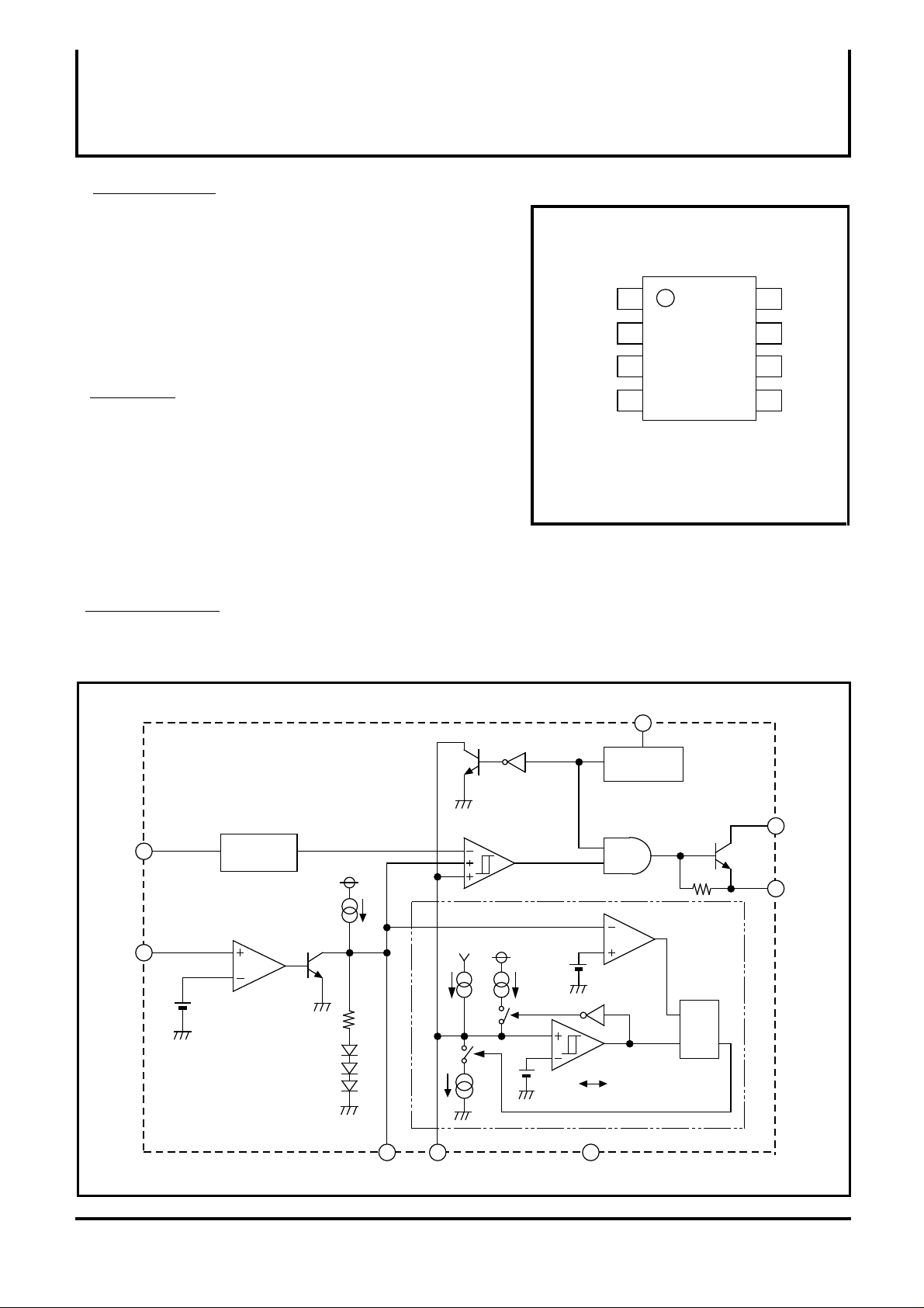
DESCRIPTION
M62212 is designed as a general purpose DC-DC converter.
This small 8 pin package contains many functions allowing
simpler peripheral circuits and compact set design.
The output transistor is open collector and emitter follower
type. This makes the control STEP-UP,STEP-DOWN and
INVERTING converter.
FEATURE
• Wide operation power supply voltage range •••••••2.5 ~ 18V
• Low power consumption••••••••••••••••••••••••1.3mA typ
• High speed switching is possible.(300kHz)
• Output short protection circuit and ON/OFF control are used.
The dead-time control and the soft-start operation are
possible
• Package variation : 8pin DIP/SOP/SSOP8
M62212P/FP/GP
GENERAL PURPOSE DC-DC CONVERTER
PIN CONFIGURATION(TOP VIEW)
Collector
output
Emitter
output
GND
Cosc
1
2
3
4
OUTLINE 8P2S-A (FP)
8P2X (GP)
8P4 (P)
M62212P /
FP / GP
8
7
6
5
VCC
IN
FB
DTC
APPLICATIONS
General electric products, DC-DC converter
BLOCK DIAGRAM
COSC
IN
4
7
OSC
VCC
OP Amp
1.25V
1.25V
PWM Comp
VCC
VCC
8
U V L O
VTH : 2.3V
Short protection
circuit
1.86V
Collector
1
output
Emitter
2
output
R
Q
S
FB
6
5
DTC
( / 8 )
1
1.15V 0.3V
3
GND
Page 2
MITSUBISHI SEMICONDUCTORS <Standard Linear ICs>
M62212P/FP/GP
GENERAL PURPOSE DC-DC CONVERTER
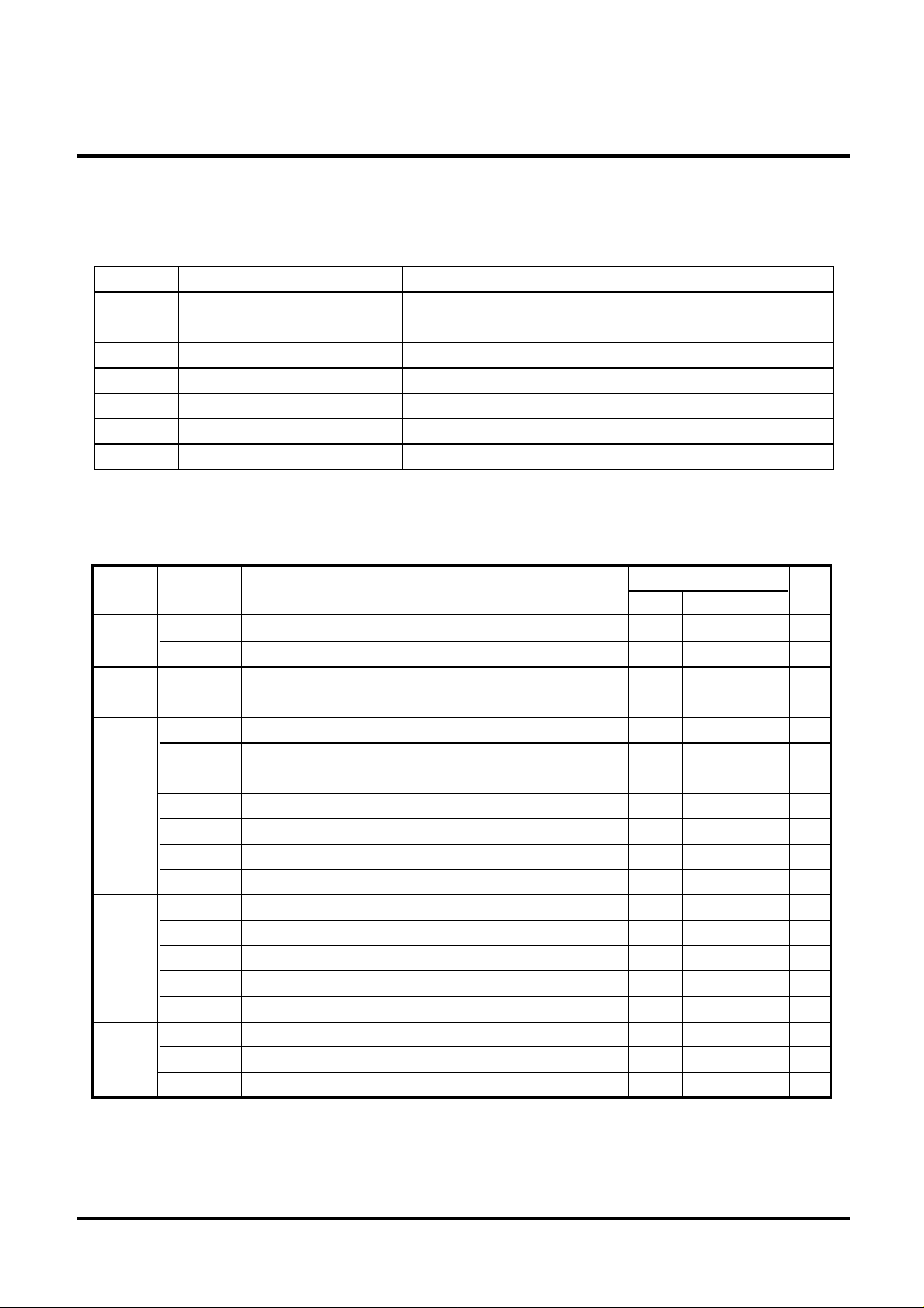
ABSOLUTE MAXIMUM RATINGS (Ta=25°C, unless otherwise noted)
Symbols Items Conditions Ratings Units
Vcc
Vo
Pd
Ktheta
Topr
Tstg
Power supply voltage
Output voltage
Output currentIo
Power dissipation
Thermal derating ratio
Operating ambient temperature
Storage temperature
Ta=25°C
Ta>25°C
19
19
150
625 (P) 360(FP) 250(GP)
5.00 (P) 2.88 (FP) 2.00(GP)
-20°C ~ +85
-40°C ~ +125
mW/°C
V
V
mA
mW
°C
°C
Electrical Characteristics ( Ta=25°C, Vcc =12V, Cosc=100pF unless otherwise noted )
Block
All
device
Std.
voltage
section
Error
amp.
section
Oscillator
section
UVLO
section
Symbol Items Test condition
VCC
I CC ST
V REF
L INE
I B
A V
G B
+
VOM
-
VOM
+
I OM
-
I OM
f OSC
VOSCH
VOSCL
I OSC CH
I OSC DIS1
VTH ON
VTH OFF
VHYS Hysteresis
Range of power supply voltage
Standby current
Standard voltage
Line regulation
Input bias current
Open loop gain
Unity gain bandwidth
Output high voltage
Output low voltage
Output sink current
Output source current
Oscillation frequency
Upper limit voltage of oscillation waveform
Lower limit voltage of oscillation waveform
Cosc charge current
Cosc discharge current 1
Start-up threshold voltage
Shut-down threshold voltage
Output "OFF" status
Voltage follower
VCC=2.5 ~ 18V
VFB=1.86V
VIN =1V
VIN =1V 2.3
VIN =1V
VHYS = VTHON - VTHOFF
Min Typ Max
2.5 18
1.19 1.25 1.31
1.82 2.62
2.2 2.4
20 80
Limits
1.3 1.8
5 12
80
0.6
6
-60 -30
110
1.0
0.45
-40
10
2.25
50
500
400
Units
V
mA
V
mV
nA
dB
MHz
V
mV
mA
uA
kHz
V
V
uA
uA
V
V
mV
( / 8 )
2
Page 3
MITSUBISHI SEMICONDUCTORS <Standard Linear ICs>
M62212P/FP/GP
GENERAL PURPOSE DC-DC CONVERTER
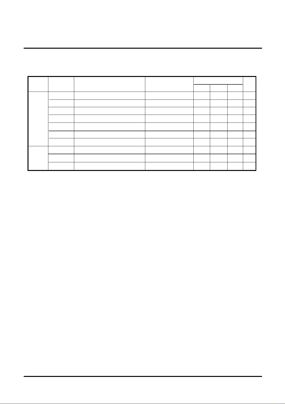
Electrical Characteristics ( Ta=25°C, Vcc =12V, Cosc=100pF unless otherwise noted )
Block
Short
protection
circuit
Output
section
Symbol
VTH FB
VTH DTC
VTL DTC
I CH1
I DIS1
I CH2
I DIS2
I CL
VSAT1
VSAT2
Items Test condition
FB threshold voltage
Latch mode "H" threshold voltage
Latch mode "L" threshold voltage
DTC charge current when start-up
DTC discharge current 1
DTC charge current when stable state
DTC discharge current 2
Collector output leak current
Collector output saturation voltage 1
Collector output saturation voltage 2
VIN =1V,VDTC=0.7V
VIN =1V,VFB =2.11V
VIN =1V,VFB =2.11V
VDTC=0.7V,VFB =2.11V
VDTC=0.7V,VFB =2.11V
VDTC=0.7V,VFB = 0.7V
VDTC=0.2V,VFB =2.11V
VCE=18V , VCC=18V
Emitter GND,
IC=150mA,VE=0V
Emitter follower,
IE=50mA,VC=12V
Limits
Min Typ Max
1.86
1.15
0.3
-45
50
-10
15
-1 1
0.3
1.6
1.1
Units
V
V
V
µA
µA
µA
µA
µA
V
V
( / 8 )
3
Page 4

MITSUBISHI SEMICONDUCTORS <Standard Linear ICs>
M62212P/FP/GP
GENERAL PURPOSE DC-DC CONVERTER
1. Application Circuit (STEP-DOWN converter with current buffer transistor)
L
VIN
D
R1
R2
2
COUT
COSC
CIN
8
4
1
M62212
VOUT
7
6 5 3
( / 8 )
4
Page 5

MITSUBISHI SEMICONDUCTORS <Standard Linear ICs>
M62212P/FP/GP
GENERAL PURPOSE DC-DC CONVERTER
2. FUNCTION DESCRIPION
1) Soft Start (The peripheral circuit is shown in Fig.1)
When the power is turned ON, input terminal IN is at 0V level. Therefore, the FB
terminal is fixed to High level. The DTC terminal goes up gradually starting from 0V
due to the internal charge current and the external CDTC.
When the level of DTC terminal reaches the lower limit of the triangular wave of the
oscillator, PWM comparator and the output circuit go into operation causing the output
voltage, "Vo" of the DC-DC converter to rise. The charge current is designed to be
approximately 45µA.
FB
DTC
OSC
OFF
External Tr collector
ON
Fig.2
2) DTC
The dead time control is set by installing a resistor between the DTC terminal and GND.
However, the DTC terminal serves as the short protection circuit also. Therefore, its set up
depends on whether the short protection circuit is used and not.
1.0V
0.45V
(When the short protection circuit is used)
At this time, the charge current for DTC is approximately 10µA . Therefore, RDTC should
be set to 40KΩ ~ 110KΩ.
(When the short protection circuit is not used)
At this time, the charge current for DTC is approximately 45µA. Therefore, RDTC is set to
12KΩÅ`25KΩ.
( / 8 )
5
Page 6

MITSUBISHI SEMICONDUCTORS <Standard Linear ICs>
M62212P/FP/GP
GENERAL PURPOSE DC-DC CONVERTER
3) Short Protection Circuit
The Short Protection Circuit used the timer latch system. It is determined by setting the
capacity used for the soft start connected to the DTC terminal.
Fig.3 shows the short protection circuit and the timing chart for various modes.
When the power is turned on, the FB terminal goes high (approx. 2.3V) and the DTC
terminal goes low (goes up slowly from 0V). Thus, approximately 45µA current will flow
when SW1:ON and SW2:OFF. The potential, namely the potential of the FB terminal is in
the amplitude of the triangular wave, SW1 will be OFF and SW2 will be ON and approximately
50µA will flow into the DTC terminal. This discharge current will cause the DTC terminal to
drop from 1.15V.
At this time, if the potential of the FB terminal goes to the control potential before the
potential at the DTC terminal goes lower than 0.45V which is the lower limit value of the
triangular wave and if the potential of the FB terminal is lower than the potential of the DTC
terminal, then the system is activated.
When the output is shorted, the system is either activated or latched depending on
whether the time for the high potential of the FB terminal reaches the potential of the control
state is long or short. (For detail, see [II] and [IV] of the Mode)
There are two ways to go back to operation after the latch to shut off output. Either
method can restart with soft start.
1. Turning ON the Vcc.
2. Make the FB terminal to go to the low potential of 1.86V or less. Then, it is
cancel led.
[Mode Explained]
[ I ] Mode •••••••••••• Activation
This is used when the FB terminal goes down to the control state potential when the DTC
terminal is in up slope. In order for the activation to occur when the DTC terminal is in down
slope, the FB terminal potential must go below the DTC terminal before the DTC terminal
goes to 0.45V.
[ II ] Mode ••••••••••••• Output short --> Activation
The system is activated if the FB terminal potential goes below the DTC terminal potential
before the DTC terminal goes to 0.45V. If there is not enough time, the output is turned OFF
(Latched)
[ III ] Mode •••••••••••• ON/OFF Control --> Activation
This mode turns off the output by forcing the DTC terminal to go down. (The system)
returns as in the case of the activation.
[ IV ] Mode •••••••••••• Output Short (Latch)
The output is turned OFF when the FB terminal potential did not go down to the control
state before the DTC terminal went down to 0.45V.
( / 8 )
6
Page 7

MITSUBISHI SEMICONDUCTORS <Standard Linear ICs>
FB
DTC
DTC set up value (Tentative)
OSC
ON
OFF
ON ON ON ON ON ON ON ON ON ON
ON
ON
ON
ON
ON ON
ONON
ON OFF OFF
OFF OFF
OFF OFF OFF OFF
OFF OFF
OFF
OFF
I 1
I 2
I 3
45µ
50µ 45µ 45µ10µ 50µ 50µ 15µ10µ 10µ
ON/OFF control --> Activate
M62212P/FP/GP
GENERAL PURPOSE DC-DC CONVERTER
Comp1
CDTC
FB
1.25V
I 1
10µ
DTC
RDTC
90KΩ
(900mV)
SW2
SW1
I 3
60µ
1.86V
Vcc
I 2
35µ
1.15V 0.3V
Comp2
(Initial RESET)
R
Q
S
* SW1 and SW2 are turned ON by "H" signal.
2.0
1.15
1.0
0.45
0
Charge Discharge
Charge
Activate
Output short
[ I ] [ II ]
Fig.3 Short Protection Circuit and the Timing Chart of the Modes
Discharge
50µ
Charge
Charge Charge Discharge
[ III ]
Charge Discharge Discharge
Output short (Latch)
[ IV ]
( / 8 )
7
Page 8

MITSUBISHI SEMICONDUCTORS <Standard Linear ICs>
M62212P/FP/GP
GENERAL PURPOSE DC-DC CONVERTER
3.CONSTANT DEFINITION
CONSTANT Step-down converter Step-up converter Inverting converter
VO + VF - VIN
VIN - VCE(sat)
1
fOSC
TON + TOFF
TON
1+
TOFF
1
-TOFF
fOSC
TON(MAX)
TON + TOFF
1
75 * 10 * fosc
(VIN -VCE(sat)) * TON(MAX) * fOSC
3
-16 * 10
2 2
-12
2 * VO * IO
VO
-1 * R2
VREF
VDTC(MAX)
| ICH1 |
VDTC(MAX)
| ICH2 |
| ICH1 | * tstart
VDTC(MAX)
IDIS1 * tshort
VDTC(MAX) -VOSCL
|Vo| + VF
VIN - VCE(sat)
1
fOSC
TON + TOFF
TON
1+
TOFF
1
-TOFF
fOSC
TON(MAX)
TON + TOFF
1
75 * 10 * fosc
(VIN -VCE(sat)) * TON(MAX) * fOSC
3
2 2
2 * VO * IO
|VO|
VREF
-1 *R2
VDTC(MAX)
| ICH1 |
VDTC(MAX)
| ICH2 |
| ICH1 | * tstart
VDTC(MAX)
IDIS1 * tshort
VDTC(MAX) -VOSCL
TON + TOFF
TOFF (MIN)
TON (MAX)
RDTC
(*4)
CDTC
(*4)
TON
TOFF
D (MAX)
COSC
L (MIN)
(*1)
R1
(*1,*2)
not use short
protection
use short
protection
calicurate from
start-up time
calicurate from
shat down time
VO + VF
VIN - VCE(sat) - VO
1
fOSC
TON + TOFF
TON
1 +
TOFF
1
-TOFF
fOSC
TON(MAX)
TON + TOFF
1
75 * 10 * fosc
(VIN - VCE(sat) - VO) * TON(MAX)
3
-16 * 10
-12
∆IO
VO
-1 * R2
VREF
VDTC(MAX)
| ICH1 |
VDTC(MAX)
| ICH2 |
| ICH1 | * tstart
VDTC(MAX)
IDIS1 * tshort
VDTC(MAX) -VOSCL
-16 * 10
-12
VF : Forward Voltage of outer Diode.
VCE(sat) : Saturation Voltage of M62212 or Saturation Voltage of Current buffer Transistor.
Åô Please setting the Oscillation frequency first and calicurate each constant value.
*1 : Please setting ŢIo about 1/3 to 1/5 of maximum output current.
*2 :|Vo|= (1+ ) * VREF
*3 : Please settng R2 about few KÉ∂ to score of KÉ∂ because output voltage don't
undergo
a influence of input current (Terminla 7).
*4 : Please setting VDTC(MAX) to satisfy D(MAX), fixed from caracteristics of D(MAX) - VDTC(MAX).
R1
R2
ICH1 means DTC charge current when start-up(-45µA typ), ICH2 means DTC charge current
when stable state(-10µA typ), VOSCL means lower limit vlage of oscillation waveform
(0.45V typ), and IDIS1 means DTC discharge current 1(50µA typ).
tstart means time internval when terminal vltage of DTC increase to VOSCL from lower voltage
and to start switching at first.
tshort means time interval when output is shut down after output is shorted.
( / 8 )
8
 Loading...