

Page 1
MITSUBISHI SEMICONDUCTORS <Standard-Linear>
GENERAL PURPOSE MULTI FUNCTION DC-DC CONVERTER
DESCRIPTION
M62211FP is designed as a general purpose multi-function
DC-DC converter. This small 10 pin package contains many
functions allowing simpler peripheral circuits and compact set
design.
The output circuit is designed OPEN-COLLECTOR output.
This makes the application for STEP-UP, STEP-DOWN and
INVERTING.
The input of this unit has two channels containing priority
control circuit. This makes the control a simple matter when
the back-light is on and during the stable state.
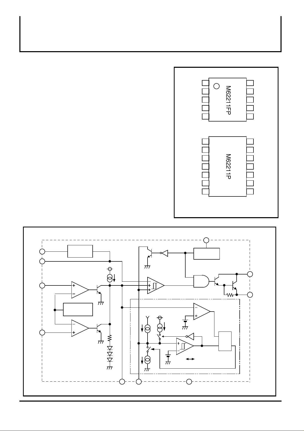
M62211P/FP
Notice: This is not a final specification.
Some parametric limits are subject to change.
PIN CONFIGURATION(TOP VIEW)
Collector
output
Emitter
output
GND
Cosc
TIN
1
2
3
4
5
OUTLINE 10P2N-A
10
Vcc
9
IN1
8
IN2
7
FB
6
DTC
FEATURE
• Wide operation power supply voltage range•••••••2.5~35V
• Operation can be synchronized by the external sync signal
• Operation can be controlled using two prioritized systems.
(High input has priority)
• High speed switching is possible.(500kHzmax)
• Output short protection circuit and ON/OFF control are used.
The dead-time control and the soft-start operation are
possible
• Small size 10-pin SOP package.
APPLICATIONS
Back-light control of personal computers and word processors
General electric products
BLOCK DIAGRAM
TIN
COSC
IN1
IN2
5
4
9
8
OSC &
sync ckt
OP Amp1
Std. voltage
1.25V
OP Amp2
VCC
1.25V
PWM Comp
VCC
Collector
output
Emitter
output
GND
Cosc
TIN
NC
NC
U V L O
VTH : 2.3V
1.86V
1
2
3
4
5
6
7
OUTLINE 14P4
NC: NO CONNECTION
VCC
10
Short protection
circuit
R
Q
S
14
13
12
11
10
9
8
1
2
Vcc
IN1
IN2
FB
DTC
NC
NC
Collector
output
Emitter
output
FB
1.15V 0.3V
7
6
DTC
( / 9 )
1
3
GND
Page 2
MITSUBISHI SEMICONDUCTORS <Standard-Linear>
Vcc
GENERAL PURPOSE MULTI FUNCTION DC-DC CONVERTER
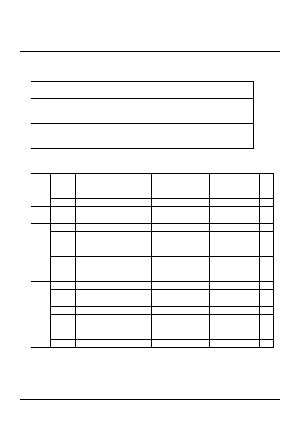
ABSOLUTE MAXIMUM RATINGS (Ta=25°C, unless otherwise noted)
Symbols
Vcc
Vo
Io
Pd
K theta
Topr
Tstg
Power supply voltage
Output current
Power dissipation
Thermal derating ratio
Operating ambient temperature
Storage temperature
Items Conditions Ratings Units
Ta=25°C
Ta>25°C
1500 (P) 450 (FP)
1.2 (P) 3.6 (FP)
M62211P/FP
36
36Output voltage
150
-20 ~ +85
-40 ~ +150
V
V
mA
mW
mW/°C
°C
°C
Electrical Characteristics ( Ta=25°C, Vcc =12V, Cosc=390pF unless otherwise noted )
Limits
Block
All
device
Std.
voltage
section
Error
amp.
section
Oscillator
section
Symbol Items Test condition Units
Vcc
Icc
VREF
LINE
IB
AV
GB
VOM+
VOM-
IOM+
IOM-
fosc
VOSCH
VOSCL
IOSC CH
IOSC DIS1
IOSC DIS2
VTINH
VTINL
Power supply voltage range
Circuit current
Standard voltage
Line regulation
Input bias current
Open loop gain
Unity gain bandwidth
Output high voltage
Output low voltage
Output sink current
Output source current
Oscillation frequency
Upper limit voltage of oscillation waveform
Lower limit voltage of oscillation waveform
Cosc charge current
Cosc discharge current 1
Cosc discharge current 2
TIN "H" level
TIN "L" level
No load
Voltage follower
Vcc=2.5 ~ 3.5V
VFB=1.86V
VFB=1.86V
VFB=1.86V
VIN1=1V, VIN2=1V
Min Typ Max
2.5 35
1.19 1.25 1.31
1.7 2.5
2.2
2.4 3.5
5 12
500
80
0.6
400
6
-100 -50
110
1.0
0.45
-120
30
120
1.0
V
mA
V
mV
nA
dB
MHz
V
mV
mA
uA
kHz
V
V
uA
uA
uA
V
V
( / 9 )
2
Page 3
MITSUBISHI SEMICONDUCTORS <Standard-Linear>
M62211P/FP
GENERAL PURPOSE MULTI FUNCTION DC-DC CONVERTER
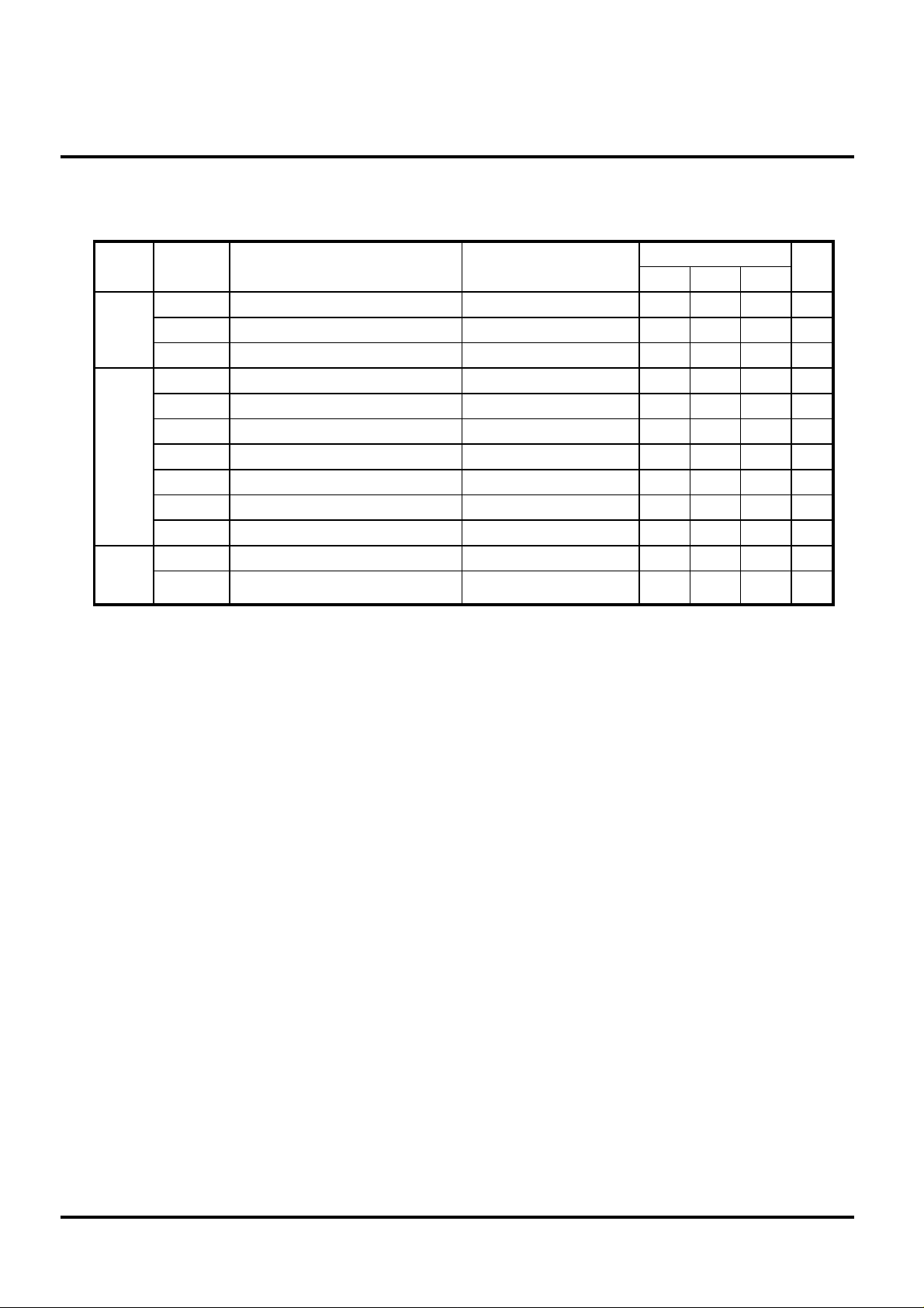
Electrical Characteristics ( Ta=25°C, Vcc =12V, Cosc=390pF unless otherwise noted )
Block
UVLO
section
Short
protec
tion
circuit
Output
section
Symbol Items Test condition
VTH ON
VTH OFF
VHYS
VTH FB
VTH DTC
VTL DTC
ICH1
IDIS1
ICH2
IDIS2
ICL
VSAT1
Start-up theshould voltage
Shut-down theshould voltage
Hysteresis
FB threshold voltage
Latch mode "H" threshold voltage
Latch mode "L" threshold voltage
DTC charge current when start-up
DTC discharge current 1
DTC charge ccurrent when stable state
DTC discharge current 2
Collector output leak current
Collector output saturation voltage
VIN1=1V, VIN2=1V, VDTC=0.7V
VIN1=1V, VIN2=1V, VFB=2.11V
VIN1=1V, VIN2=1V, VFB=2.11V
VDTC=0.7V, VFB=2.11V
VDTC=0.7V, VFB=2.11V
VDTC=0.7V, VFB=0.7V
VDTC=0.2V, VFB=2.11V
VCE=35V, Vcc=35V
Emitter follower,
IE=50mA, Vc=12V
Limits
Min Typ Max
Units
2.2 2.42.3
2.25 V
20 8050 mV
1.86 V
1.15 V
0.3 V
-35 µA
45 µA
-15 µA
20 µA
-1 1 µA
V
V1.6
( / 9 )
3
Page 4

1. Explanation of Back Light Control Circuit
VCC
Cl
OSC &
sync ckt
Cosc
IN1
IN2
OP Amp1
Std. voltage
1.25V
OP Amp2
MITSUBISHI SEMICONDUCTORS <Standard-Linear>
M62211P/FP
GENERAL PURPOSE MULTI FUNCTION DC-DC CONVERTER
VR1
R4
DC/AC
R3
CDELAY
FL
Tube
D2
RFL
CFL
U V L O
TH
V :2.3V
R
S Q
D1
Co
R1
R2
RDTC
CDTCCf1Cf2
Rl1
Rl2
Fig.1 An Application of the Back Light Control Circuit
1-1. Priority Control Operation
As far as OPAmp1 and OPAmp2 are concerned, there is no problem when either IN1 or IN2 is
used to control current, since the setting up to lower the output voltage of the DC-DC converter is
prioritized. (The above figure uses IN1 to control current.)
1) When starting, the output voltage "Vo" is determined by the feedback to IN2 via R1 and
R2 and the following equation :
Vo=VREF * (R1 + R2)/R2 (VREF =1.25Vtyp) (Area of the Timing Chart 1)
2) Next, this output voltage "Vo" is used to discharge the FL tube by the inverter and causes
the tube current to flow. The tube current is filtered and smoothed by RFL, D2, and CFL so
that the DC voltage (VCFL) corresponding to the tube current is generated at CFL.
The voltage of VCFL is divided by R3, VR1, and R4, and feedback to IN1, it can control tube
current. (Area of the Timing Chart 2)
3) Here, CDELAY is inserted between R3 and VR1 + R4 in order to regulate the timing to switch
from the voltage control to the current control. (Area of the Timing Chart 3)
4) When in the current control state, it is possible to adjust brightness by changing the
amount of feedback of the tube current using VR1. (Area of the Timing Chart 4)
5) If the feedback used for controlling current is lost due to irregularities in the FL tube. etc..
the control returns to the voltage control mode. (Area of the Timing Chart 5)
( / 9 )
4
Page 5

<Timing Chart>
(V)
MITSUBISHI SEMICONDUCTORS <Standard-Linear>
M62211P/FP
GENERAL PURPOSE MULTI FUNCTION DC-DC CONVERTER
(mArms)
(V)
(V)
III
( / 9 )
5
II
IV
VI
Page 6

MITSUBISHI SEMICONDUCTORS <Standard-Linear>
M62211P/FP
GENERAL PURPOSE MULTI FUNCTION DC-DC CONVERTER
1-2 Setting Up TIN
1) Setting Up the Level
The TIN terminal is shown in Fig.a. In order for the level of TIN to satisfy the conditions shown in
the table below, the external circuits shown in Fig.b or Fig.c should be used when the external
voltage level of the input is high.
100KΩ
5
TIN
50KΩ
5 5
3
GND
Fig.a
Items
TIN "H" level
TIN "L" level
2) Setting Up frequency
The periodical change of TIN is expected to be +30% ~ -20%. The fIN is set to
approximately 1.5 times fOSC
Symbols Unitmin
VTINH
VTINL
2.2
fIN = 1.5 * fOSC
fsoc ≈
Fig.b Fig.c
typ max
VCC
1.0
1
1.3µs+(23 * 10 * Cosc )
3
(Hz)
V
V
COSC
TIN
( / 9 )
6
Page 7

MITSUBISHI SEMICONDUCTORS <Standard-Linear>
M62211P/FP
GENERAL PURPOSE MULTI FUNCTION DC-DC CONVERTER
1-3 Soft Start, DTC, and Short Protection
1) Soft Start (The peripheral circuit is shown in Fig.1)
When the power is turned ON, IN1 and IN2 are at 0V level. Therefore, the FB terminal
is fixed to High level. The DTC terminal goes up gradually starting from 0V due to the
internal charge current and the external CDTC.
When the level of DTC terminal reaches the lower limit of the triangular wave of the
oscillator, PWM comparator and the output circuit go into operation causing the output
voltage, "Vo" of the DC-DC converter to rise. The charge current is designed to be
approximately 35µA.
FB
DTC
OSC
OFF
External Tr collector
ON
Fig.2
2) DTC
The dead time control is set by installing a resistor between the DTC terminal and GND.
However, the DTC terminal serves as the short protection circuit also. Therefore, its set up
depends on whether the short protection circuit is used and not.
(When the short protection circuit is used)
1.0V
0.45V
At this time, the charge current for DTC is approximately 10µA . Therefore, RDTC should
be set to 40KΩ ~ 110KΩ.
(When the short protection circuit is not used)
At this time, the charge current for DTC is approximately 45µA. Therefore, RDTC is set to
12KΩ ~ 25KΩ.
( / 9 )
7
Page 8

MITSUBISHI SEMICONDUCTORS <Standard-Linear>
M62211P/FP
GENERAL PURPOSE MULTI FUNCTION DC-DC CONVERTER
3) Short Protection Circuit
The Short Protection Circuit used the timer latch system. It is determined by setting the
capacity used for the soft start connected to the DTC terminal.
Fig.3 shows the short protection circuit and the timing chart for various modes.
When the power is turned on, the FB terminal goes high (approx. 2.4V) and the DTC
terminal goes low (goes up slowly from 0V). Thus, approximately 35µA current will flow
when SW1:ON and SW2:OFF. The potential, namely the potential of the FB terminal is in
the amplitude of the triangular wave, SW1 will be OFF and SW2 will be ON and approximately
45µA will flow into the DTC terminal. This discharge current will cause the DTC terminal to
drop from 1.15V.
At this time, if the potential of the FB terminal goes to the control potential before the
potential at the DTC terminal goes lower than 0.45V which is the lower limit value of the
triangular wave and if the potential of the FB terminal is lower than the potential of the DTC
terminal, then the system is activated.
When the output is shorted, the system is either activated or latched depending on
whether the time for the high potential of the FB terminal reaches the potential of the control
state is long or short. (For detail, see [II] and [IV] of the Mode)
There are two ways to go back to operation after the latch to shut off output. Either
method can restart with soft start.
1. Turning ON the Vcc.
2. Make the FB terminal to go to the low potential of 1.25V or less. Then, it is
cancel led.
[Mode Explained]
[ I ] Mode •••••••••••• Activation
This is used when the FB terminal goes down to the control state potential when the DTC
terminal is in up slope. In order for the activation to occur when the DTC terminal is in down
slope, the FB terminal potential must go below the DTC terminal before the DTC terminal
goes to 0.45V.
[ II ] Mode •••••••••••• Output short --> Activation
The system is activated if the FB terminal potential goes below the DTC terminal potential
before the DTC terminal goes to 0.45V. If there is not enough time, the output is turned OFF
(Latched)
[ III ] Mode ••••••••••• ON/OFF Control --> Activation
This mode turns off the output by forcing the DTC terminal to go down. (The system)
returns as in the case of the activation.
[ IV ] Mode ••••••••••• Output Short (Latch)
The output is turned OFF when the FB terminal potential did not go down to the control
state before the DTC terminal went down to 0.45V.
( / 9 )
8
Page 9

MITSUBISHI SEMICONDUCTORS <Standard-Linear>
M62211P/FP
GENERAL PURPOSE MULTI FUNCTION DC-DC CONVERTER
Comp1
CDTC
FB
FB
1.25V
I 1
10µ
DTC
RDTC
90KΩ
(900mV)
SW2
SW1
I 3
55µ
1.86V
Vcc
I 2
25µ
1.15V 0.3V
Comp2
(Initial RESET)
R
Q
S
* SW1 and SW2 are turned ON by "H" signal.
2.0
1.15
1.0
0.45
0.20
0
I 1
I 2
I 3
DTC
ON
ON ON ON ON ON ON ON ON ON ON
ON OFF OFF
OFF
Charge Discharge
45µ 35µ 35µ10µ 45µ 45µ 20µ10µ 10µ
35µ
OFF OFF OFF OFF
Charge
Activate
[ I ] [ II ]
OFF OFF
ONON
Discharge
45µ
Output short
Charge
ON ON
OFF OFF
ON
Charge Charge Discharge
ON/OFF control --> Activate
[ III ]
DTC set up value (Tentative)
OFF
OFF
Charge Discharge Discharge
ON
ON
ON
Output short (Latch)
[ IV ]
OSC
Fig.3 Short Protection Circuit and the Timing Chart of the Modes
( / 9 )
9
 Loading...