

Page 1
3V POWER SUPPLY with WATCHDOG TIMER
GENERAL DESCRIPTION
M62055FP is a 3V power supply featuring a watchdog
timer function for a microcontroller system.
It can be a power source of 3V ± 5% by utilizing the
reference voltage and amplifier.
It can also generate a reset pulse for the applied
systems during power-on, moreover it includes the
watchdog timer for a self diagnostics of the system,
which can prevent system erroneous functions.
FEATURES
• Power-on reset
• Watchdock timer
• High accuracy voltage source of 3V ±5% (max)
• Overcurrent protection circuit
• The voltage detection accuracy of ±5% (max)
• Output power (Vo) cutoff function at erroneous
conditions
• Backward voltage protection circuits for inputs and
outputs
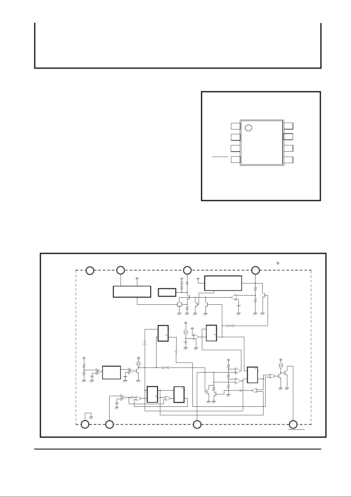
MITSUBISHI<Dig./Ana.INTERFACE>
M62055FP
PIN CONFIGURATION(TOP VIEW)
GND
WD
RESET
Outline 8P2S
M62055FP
Vcc
CLM
VDDTC
VOC
APPLICATION
Handy information terminal equipment, CD-ROM, Portable audio
equipment.
BLOCK
DIAGRAM
Vcc
Vref
.
=1.25v
.
CLM
VOLTAGE DETECTOR
(CURRENT LIMITER)
RISE DELAY
(300µsec)
Vref
.
=1.5v
.
Vref
.
=1.5v
.
VD
Vcc
START
CIRCUIT
Set priority
Q
QRS
Reset
priority
Q
QRS
Reset
priority
Vcc
Vcc
Vcc
Reset priority
Vref
.
=0.9v
.
QRS
Q
The input and
output reversal
conservation circuit
RSQ
Q
56K
40K
Vref
=1.25v
Set priority
R Q
VO
Note ; It indicates Vo,
QS
unless otherwise noted
MITSUBISHI
( / 6 )
1
TCWDGND
RESET
970508
Page 2
Pin Functional description
MITSUBISHI<Dig./Ana.INTERFACE>
M62055FP
3V POWER SUPPLY with WATCHDOG TIMER
pin number
3
4 Reset signal output
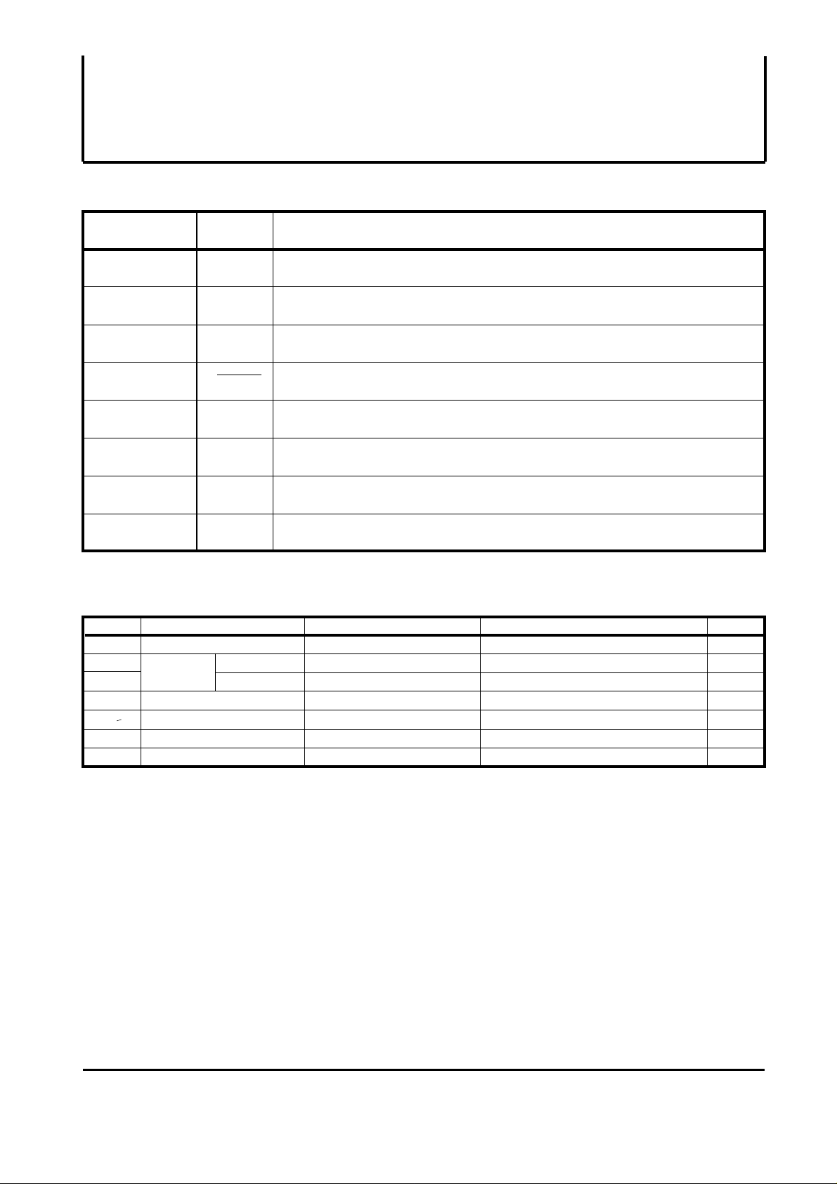
ABSOLUTE MAXIMUM RATINGS
symbol Parameter conditions Ratings Unit
Vcc
VRM
IRM
VWDM
Topr
supply voltage
Reset pin
Watchdock pin input voltage
Ko
Thermal derating
Operating temperature
Storage temperature
symbol Functional description
GND1
WD2
TC
RESET
VO5 Feedback to a power supply for a MCU.
VD6
CLM7 Current limiting
Vcc8 Power supply voltage
Output voltage
Output current
Ground
Input for watchdock timer.
Setting up reset timer and watchdock timer.
Controlling the stability of an output voltage with a PNP transistor
connected externally.
(Ta=25°C, Unless otherwise noted)
Ta ≥ 25°C
13
10
10
3
4.0
- 20 ~ + 75
- 55 ~ + 150
mA
mW/°C
°C
°CTstg
V
V
V
MITSUBISHI
( / 6 )
2
970508
Page 3

MITSUBISHI<Dig./Ana.INTERFACE>
M62055FP
3V POWER SUPPLY with WATCHDOG TIMER
ELECTRICAL CHARACTERISTICS
(Vcc=5.0V,Ta=25°C, Unless otherwise noted)
(1) DC CHARACTERISTICS
symbol
Parameter
Test conditions
Min
Limits
Typ
Max
Unit
Battery• back up• regulator
VCC
ICC
VO
IBmax
I BSC
Reg-in
Reg-lo
∆Vo/∆T
VTHCLM 200 mV
supply voltage
Circuitry current
Output voltage
Bias current
Listing short-circuit bias current
Input voltage regulation
Loading voltage regulation
Output voltage thermal coefficient
CLM threshold voltage
Vcc=3.5V~13V
Io=10mA~100mA
3.5 13
650
2.85 3.0
950
3.15
10
1.5
0.02
0.25
1
0.02
180 220
%/V
25
%/T
Reset, watch dock timer
VTH1(H)
VTH1(L)
∆VTH1
VOL(RST)
Ileak
VTH2(H)
VTH2(L)
IWD
VTH(WD)
Itco
Itc1
Itc2
VCCMIN
Vo detection voltage
Output voltage
Output leakage current
Reset
pin
Watchdock timer
threshold voltage
WD input current
WD input threshold voltage
TC output current
TC input current
Vcc min operating voltage
2.68
2.58
Isink=4mA
2.28 2.4 2.52
0.95 1.0 1.05
VIN=3V
VIN=0.8V
VIN=2.4V
In the output cutoff transmission mode
8.0
*1 2.0
2.82
2.72
2.96
2.86
0.1
0.2 0.4
1.5
2.0
5
1
1
V
µA
V
mA
mA
mV
V
V
V
V
µA
V
V
µA
V
µA
mA
mA
V
Note *1; The Vcc minimum operating voltage at which the RESET output is Low
(2) AC CHARACTERISTICS (Vcc=5.0V,Ta=25°C, Unless otherwise noted)
symbol
tWD
tRST(1)
tRST(2)
Parameter
Watch dock timer
Reset timer (1)
Reset timer (2)
Test conditions
C=0.1µF,R1=10KΩ
Min Typ
0.5 1.2
C=0.1µF,R1=10KΩ mS
CO=10µF, R1=10KΩ, IL=0
0.1
Limits
MITSUBISHI
( / 6 )
3
0.7
Max
1.7
2.0
Unit
mS
mS
970508
Page 4

4
FUNCTIONAL DESCRIPTION
VO+VCE(sat)
Vcc
0
output cutoff output cutoff
Vo
TC
VTH1(H)
0
VTH2(H)
VTH2(L)
0
VTH1(L)
.
=0.9V =0.9V
.
Tick deactivation
.
.
MITSUBISHI<Dig./Ana.INTERFACE>
M62055FP
3V POWER SUPPLY with WATCHDOG TIMER
RESET
0
WD
0
1 3
2
TRST(1)
456 789 10 11 12 13 14
TWD
TRST(2)
1 : When Vo rises to 0.5 V, RESET becomes
low. Then, charging to a capacitor C
connected to TC will be started at the Vo
of 2.82V(VTH1(H)).
2 : When VCC rises to 3V+VCE(sat), Vo
becomes stable.
3 4 : When TC voltage rises to 1V(VTH2(L)) ,
RESET becomes high. When it rises to
2.4V (VTH2(H)) further, the capacitor C is
switched to discharge and RESET
becomes low.
5 : At the same time of a change-over to the
discharge from the capacitor C, Vo is
intercepted.
Then,TC will be discharged completely at
Vo of 2.72V(VTH1 (L)).
6 : Vo returns to 3V right after it has fallen
down to 0.9 V.
RESET repeats above operation till a
normal clock signal is input to WD pin.
7 8 : In the case of a sudden power interruption, Vo
9 falls down according to a decrease of VCC.
When it falls down to 2.72V, the capacitor C is
discharged and RESET will be low.
In the case of a reversion from the power
interruption, Vo rises according to a increase of
VCC. When it rises to 2.82V, the charging to the
capacitor C is started and RESET will be high
right after TC voltage reaches 1V.
10 11 : In the case a clock signal for discharging the
capacitor C is applied to pin WD before TC
voltage reaches to 2.4V, a reset signal to
RESET is canceled.
12 13 : In the case an abnormal clock signal is input,
TC repeats charging / discharging alternately
between 1 V and 2.4 V, so that RESET also
repeats high / low till a normal clock signal is
input.
14 : When Vo falls down to 2.72 V, RESET becomes
Low.
MITSUBISHI
( / 6 )
970508
Page 5

MITSUBISHI<Dig./Ana.INTERFACE>
t1
t2
tWDIN
XV
VTH2(H) = 2.4v
VTH2(L) = 1.0v
Pin 3
Pin 2
1.2 • C • R1
1
< f
5
1. Pin 3 (TC pin) Charging and discharging
time .
When an error is occurred in WD input,
TC waveform is as shown below.
(Charging time)
The following formula can be obtained because
tRST(2) is equal to the duration of Vo cutoff.
2. Pin 2 (WD pin) Input frequency,
input pulse width, charge/discharge
time .
Conditions of an input to pin 2 (WD pin)
(1) Input period should be tWD or less.
( Pin discharge is completed before the arrival
of VTH2(H) = 2.4 V )
(2) Input pulse width tWDIN should be t2 or less.
cutoff Tr
output cutoff
0
0
Vo
TC
VTH1(H)
VTH1(L)
=0.9V
VTH2(H)
VTH2(L)
tRST(1)
tWD
tRST(2)
Inside delay time
tRST(1) = 0.406 • C • R1
+ 300µs
*1
*1 : Inside delay time (Typical values)
DESCRIPTION of TERMS
tRST(1)
tWD
tRST(2)
Time from when TC is VTH2(L) until it
reaches to VTH2(H).
Time from when TC begins to charge
until it reaches to VTH2(L).
*2 : Inside delay time
(Typical values)
Time from when TC is VTH2(H) until TC
starts charging.
*3 : R = Internal resistance
t1 = C • R1 • ln
2
3-X
t2 = 1000 • C • R1 • ln
1000
R1
- 2
X ( + 1)
- 3
1000
R1
tRST(2) = C • R • ln (
3
0.9
)
= 40 • C + 300µs
*2
*3
+ 300µs
*2
.
.
When input of 2 WD is normal, TC waveform 3
is as shown below.
M62055FP
3V POWER SUPPLY with WATCHDOG TIMER
VO = 3.0V
tWD = 1.2 • C • R1
R1
3
C
Al
C
MITSUBISHI
( / 6 )
970508
Page 6

3. Relationship between the input
2.4v2.4v
1.0v tWD
VIN
WD
TC
RESET
t
t
t
t
3.0v
t 3 = -C • R • ln
VIN
1.5v
Addition of a low pass filter makes input
waveform dull. An input pulse width and CR
of a low pass filter is determined referring to
the right figure.
If t3 is too long, the TC waveform changes as
shown in the diagram above.
t3 is set as follows; tWDIN (3 µs) or more and t 2
(charging time) or less.
(t2 is a discharge time while an input is normal)
pulse width and the low pass filter
V0
R
3.0V
0.0V
VIN
filter
(External Element)
1K
WD
-
C
+
1.5V
MITSUBISHI<Dig./Ana.INTERFACE>
M62055FP
3V POWER SUPPLY with WATCHDOG TIMER
1.5v
t3
t4
RESET is output in the case of t 4> t WD.
APPLICATION
VCC 10µF
CIN
+
VCC CLM VD VO
GND
M62055FP
WD TC
RESET
RTC
CO
+
10µF
GND
CLOCK
MCU/MPU
CTC
RESET
RRST
VDD
Note : hFE of the external PNP transistor, 100 to 300 is recommended.
MITSUBISHI
( / 6 )
6
970508
 Loading...