

Page 1
MITSUBISHI<Dig./Ana.INTERFACE>
M62050P,FP
3V supply SYSTEM RESET with watchdog timer
GENERAL DESCRIPTION
M62050P/FP is a voltage threshold detector designed for detection
of 3V supply voltage and generation of a system reset pulse. It is
suitable for microcontroller systems.
The IC, a supervisor of the MCU operations, dissipates low current
of 0.6mA (typ) during normal operations of the MCU systems.
It has 2 selectable threshold voltages, which allows applying it to a
high precision system design.
FEATURES
• Watchdog timer (supervisor for 2 system voltages)
• Power-on reset timer
• Low current consumption 0.6mA (typ) at Vcc = 3V
• Wide supply voltage range Vcc = 7V (max)
APPLICATION
• Supervisor for microcontroller systems
RECOMMENDED OPERATING CONDITION
• Supply voltage range 2V ~ 4V
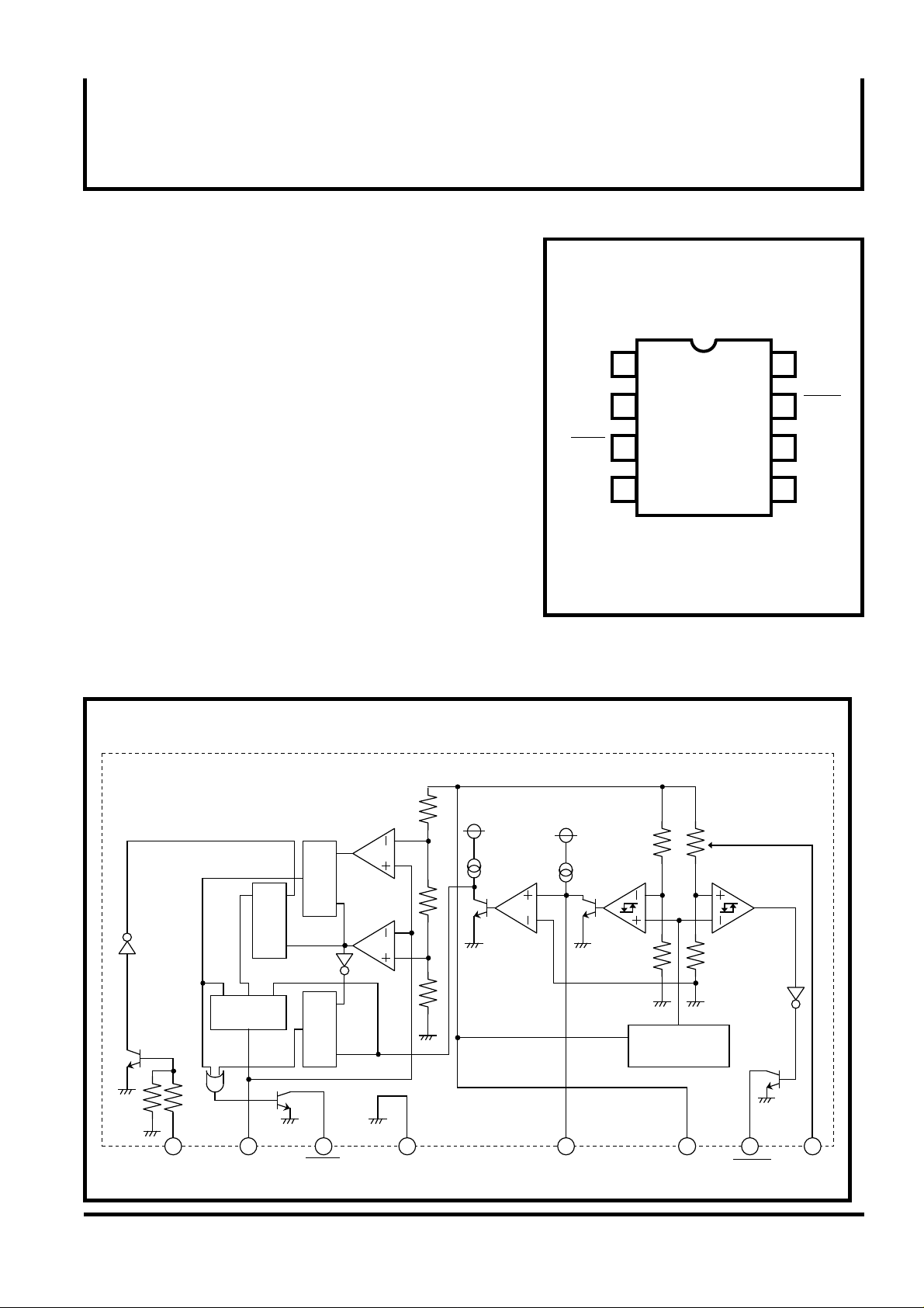
PIN CONFIGURATION(TOP VIEW)
1
WD
2
TC
RST1
3
4
GND ct1
OUTLINE 8P4(P)
8P2S-A(FP)
M62050P,FP
8
ADJ
7
RST2
6
Vcc
5
BLOCK DIAGRAM
W•D•T
WD TC GND Vcc ADJRST2ct1RST1
F•F
F•F
F•F
2 543 61 7 8
1.24V
REFERENCE
VOLTAGE
CIRCUIT
( / 4 )
1
1995-12-6
Page 2
MITSUBISHI<Dig./Ana.INTERFACE>
M62050P,FP
3V supply SYSTEM RESET with watchdog timer
Terminal functional description
PIN No. symbol Terminal functional description
1
2
3
4
5
6
7
8
ABSOLUTE MAXIMUM RATING
symbol Parameter Ratings Units
W D
T C
RST1
GND
ct1
Vcc
RST2
ADJ
Input for watchdog timer
Time set for reset timer and watchdog timer
When abnormal signaling is input into WD terminal, it
generates reset signal.
GND
Detection voltage adjustment for WD input
Power supply
When power supply voltage became abnormal, it generates
reset signal.
Selection between 2 detection voltages
VCC
VIN
VOUT
IOUT
Pd
KO
Topr
Tstg
Power supply voltage
Input voltage
Output voltage
Output current
Internal power dissipation
Heat reduction rate
Operating ambient temperature
Storage temperature
( / 4 )
15
-0.3 ~ 5
15
10
625
4.40
-20 ~ +75
-55 ~ +125
2
V
V
V
mA
mW
mW/°C
°C
°C
Page 3

MITSUBISHI<Dig./Ana.INTERFACE>
M62050P,FP
3V supply SYSTEM RESET with watchdog timer
ELECTRICAL CHARACTERISTIC (Ta=25 °C, VCC=3V, unless otherwise noted)
(1) DC characteristics
Symbol Parameter
IWD
WD input current
Terminal
WD
Measurement condition
VIN=3V
Ratings
MIN TYP MAX
0.15
0.06 0.25
Unit
mA
VIH
VIL
IOUT
IIN
VTH3(H)
VTH3(L)
VOL
Ileak
VTH1(H)
∆TH1
VTH2(H)
VTH2(L)
∆VTH2
RST1
RST2
ICC
WD input voltage
TC output current
TC input current
Watchdog timer
threshold voltage
Output voltage
Output leakage current
Vcc detection voltage(2)
RST1 ON voltage
RST2 ON voltage
Circuit current
WD
TC
TC
TC
RST1
RST2
VCC1Vcc detection voltage(1)VTH1(L)
VCC2
RST1
RST2
VCC
VIN=0.9V
VOUT=2.5V
IOUT=1mA
VOUT=4V
ADJ Terminal=OPEN
ADJ Terminal=Vcc
ADJ Terminal=OPEN
ADJ Terminal=Vcc
VCC=1.2V,RL=3kΩ
VCC=1.2V,RL=3kΩ
1.5 3.00
-0.3
0.80
-0.10
2.50
2.00
5.00 µA
2.382.252.13
2.302.202.10
0.080.050.03
2.682.552.43
2.602.502.40
0.080.050.03
0.5
0.5
0.5
1.0
V
V
µA
mA
V
V1.00
V0.500.20
V
V
V
V
V
V
V
V
mA
(2) AC characteristics
Symbol Parameter
TWD
tRST(1)
tRST(2)
tWDIN
td1
Watchdog timer
Reset Timer(1)
Reset Timer(2)
Input pulse duration
Propagation delay
td2
Terminal
RST1
RST1
RST1
WD
RST1
RST2
( / 4 )
Measurement condition
C=0.1µF,R1=10kΩ
C=0.1µF,R1=10kΩ
R1=10kΩ
C=0.1µF,R1=10kΩ
3
Ratings
MIN TYP MAX
1.1CR1
0.5
0.2
40
1.1
0.5CR1
830C
1.7
1.10.50
22083
3
10
5
Unit
s
ms
s
ms
s
µs
µs
µs
µs
Page 4

Timing chart
MITSUBISHI<Dig./Ana.INTERFACE>
M62050P,FP
3V supply SYSTEM RESET with watchdog timer
VCC
TC
VIN
RST1
0V
VTH3(H)
VTH3(H)
0V
0V
0V
VTH2(H)
VTH1
VTH2(L)
VTH1
RST2
0V
tRST(1) tWD tRST(2)
Application circuitry example
CLOCK
8 7 6 5
M62050
1 2 3 4
RST1
(RESET)
MCU/MPU
RST2
(HOLD)
( / 4 )
4
VDD
 Loading...