

Page 1
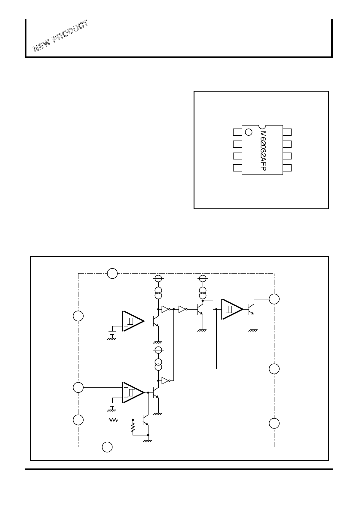
GENERAL DESCRIPTION
The M62032AFP is an IC for detection of two different input
voltages to reset almost all logic circuits including MCU.
It contains a delay circuit with which any delay time can be
obtained only by adding an external capacitor.
The IC is widely applicable to a battery check circuit, a level
detection circuit, a waveform shaping circuit, etc.
FEATURES
• A small number of external components
• Built-in 2 input voltage detection circuits
• Wide supply voltage range ............... 2 to 10V
• Small 8-pin package
• Open collector output
APPLICATION
Reset circuit of MPU, MCU and logic
RECOMMENDED OPERATING CONDITION
Supply voltage range ......................... 2 to 10V
MITSUBISHI<STD-LINEAR>
M62032AFP
VOLTAGE DETECTING, SYSTEM RESETTING IC
PIN CONFIGURATION (TOP VIEW)
BLOCK DIAGRAM
VCC
7
Vcc
Vcc
VIN1
1
VIN2
2
3
N C
GND
4
OUTLINE 8P2S(FP)
8
VRES
7
VCC
VO
6
EXTERNAL
5
CAPACITOR
VO
6
2
VIN2
1.25V
Vcc
VIN1
VRES
1
1.25V
8
4
GND
( 1 / 4 )
Delay
5
Capacitor C
NC
3
Page 2
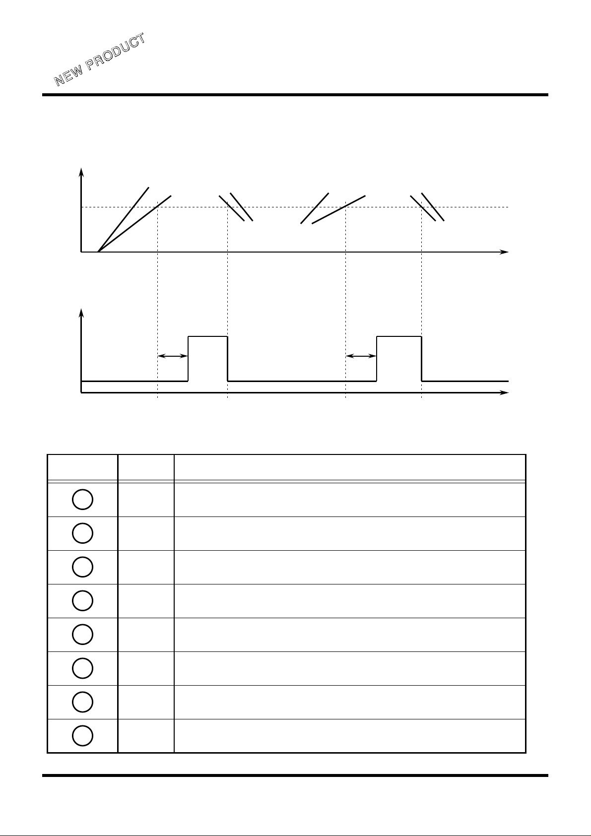
FUNCTIONAL DIAGRAM
MITSUBISHI<STD-LINEAR>
M62032AFP
VOLTAGE DETECTING, SYSTEM RESETTING IC
INPUT
VOLTAGE
INPUT1
1.25V
OUTPUT
H
L
TERMINAL DESCRIPTION
INPUT 2
TPLH1
INPUT1
INPUT 2
INPUT 2
INPUT1
INPUT1
INPUT 2
t
TPLH1
t
Terminal No. Symbol Functional Description
1
2
3
VIN1
VIN2
NC
4 GND
5
6
7
8
EXTERNAL
CAPACITOR
Vo
VCC
VRES
Detecting voltage input 1
Detecting voltage input 2
No connection
Ground
Delay capacitor connection
Output (open collector)
Supply voltage
It outputs "L" and "H" to the Vo terminal when VRES input is "H" and "
L", respectively.
( 2 / 4 )
Page 3

MITSUBISHI<STD-LINEAR>
VOLTAGE DETECTING, SYSTEM RESETTING IC
ABSOLUTE MAXIMUM RATINGS (Ta=25 ˚C, unless otherwise noted)
Symbol Parameter Conditions UnitRatings
M62032AFP
VCC
ISINK
VO
VRES
Pd
Ktheta
Topr
Tstg
Supply Voltage
Output Sink Current
Output Voltage
Self Reset Input Voltage
Power Dissipation
Thermal Derating
Operating Temperature
Storage Temperature
Ta ≥ 25˚C
10
8.0
10
10
300
3.0
-20 to +75
-40 to +125
ELECTRICAL CHARACTERISTICS (Ta=25 ˚C, unless otherwise noted)
<Reset circuit1>
Symbol Parameter Test Conditions
VS1
∆VS1
VIN
IIN
IPD
VOL1
∆VSCin
* The delay time can be varied by changing the connecting capacitance(Cd).
Tpd = CV/I = Cd x 1E6 (sec)
<Reset circuit2>
Symbol Parameter Test conditions Unit
VS2
∆VS2
VIN
IIN
<Common specification>
Symbol
Detecting Voltage 1
Hysteresis Voltage 1
Input Voltage Range
Input Current
Constant Current
Low Output Voltage 1
Delay Timetpd1 Cd=0.01uF
Maximum Delay Timetpdmax
Delay Capacitor part
Hysteresis Voltage
Detecting Voltage2
Hysteresis Voltage2
Input Voltage Range
Input Current
Parameter Test conditions
VCC ≤ 7V
VCC>7V -0.3
VIN=1.25V
IOL=5mA
VCC ≤ 7V
VCC>7V
VIN=1.25V
Min Typ Max
1.20
-0.3
Min Typ Max
1.20 1.25
-0.3
-0.3
Min Typ Max
VCC Supply Voltage Range
ICC1
VS/∆T
∆VS/∆T
TPLH/∆T
IOH
TPHL CL=100pF
VOPL
VRESH
IRESH
VRESL
Circuit Current in OFF
Detecting Voltage Temperature
Coefficient
The Hysteresis Voltage
Temperature Coefficient
Propagation Delay Time
Temperature Coefficient
Output Leak Current
Output "L" Propagation Delay Time
Threshold Operating Voltage
Input "HIGH" voltage
VRES
Input "HIGH" current
Input "LOW" voltage
VCC=5V
RL=2.2kΩ,VOL ≤ 0.4V
RL=100kΩ,VOL ≤ 0.4V
VRES=2V
Limits
1.25
9 15
100
-1.4
0.2
10
680 1130Cd=0.68uF
250 mV
Limits
9 15
100 500
Limits
2
0.3
0.01
0.01
0.10
10
0.67
0.55
2 VCC V
1.30
23
VCC
7.0
500
0.4
1.30
23
VCC
7.0
10
0.6
0.8
0
0.70
0.8-0.3
V
mA
V
V
mW
mW/˚C
˚C
˚C
Unit
V
mV
V
nA
uA
V
mS
V
mV
V
nA
Unit
V
mA
%/°C
%/°C
%/°C
1
uA
us
V
uA80
V
( 3 / 4 )
Page 4

VOLTAGE DETECTING, SYSTEM RESETTING IC
AN EXAMPLE OF THE APPLICATION CIRCUIT
MITSUBISHI<STD-LINEAR>
M62032AFP
VCC
DETECTION
INPUT 1
DETECTION
INPUT 2
Interrupt
Input signal
* A forced reset signal (high) into pin 8 from outside can reset this IC (low output) regardless of input
signals to pins 1 and 2.
7
1
6
M62032AFP
2
8
4
EXTERNAL
CAPACITOR
5
RL
RESET (RESET)
MCU
0.01uF
Supply Voltage
GND
!
Mitsubishi Electric Corporation puts the maximum effort into making semiconductor products better and more
reliable, but there is always the possibility that trouble may occur with them. Trouble with semiconductors may
lead to personal injury, fire or property damage. Remember to give due consideration to safety when making
your circuit design, in order to prevent fires from spreading, redundancy, malfunction or other mishap.
( 4 / 4 )
 Loading...