

Page 1
VOLTAGE DETECTING, SYSTEM RESETTING IC SERIES
GENERAL DESCRIPTION
The M62030FP is a voltage threshold detector designed for
detection of an input voltage/supply voltage and generation of
a system reset pulse for almost all logic circuits such as
microcontroller.
It contains a delay circuit which provides 200µs (typ) delay
and 4 modes of delays [25ms, 50ms, 100ms, 200ms (typ)] in
the input voltage detection type and in the supply voltage
detection type, respectively.
FEATURES
• Built-in 2 functional circuits for detecting voltage
• Built-in delay circuit to provide long delay time
(without external delay capacitors)
• Selectable 4 modes of delay time
[25msec, 50msec, 100msec, 200msec(typ)]
• Few external components
• Small 8-pin SOP package
MITSUBISHI<Dig./Ana. INTERFACE>
M62030FP
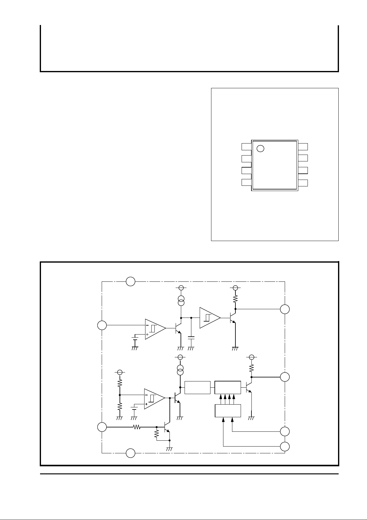
PIN CONFIGURATION (TOP VIEW)
1 VRES
Ct0
VIN
2
Ct1
3
GND
4
M62030FP
8
7
6
5
Vcc
OUT1
OUT2
APPLICATION
• Reset circuits of MCU, MPU and logics
RECOMMEND OPERATING CONDITION
• Supply voltage range ………… 2V to 10V
BLOCK DIAGRAM
Vcc
7
VIN
2
1.25V
Vcc
Vcc
OSCILLATOR
FREQUENCY
DIVIDER
Outline 8P2S-A
Vcc
VccVcc
6
OUT1
OUT2
5
VRES
1.25V
8
MULTIPLEXER
3
Ct1
1
Ct0
4
GND
1
( / 5 )
Page 2
MITSUBISHI<Dig./Ana. INTERFACE>
M62030FP
VOLTAGE DETECTING, SYSTEM RESETTING IC SERIES
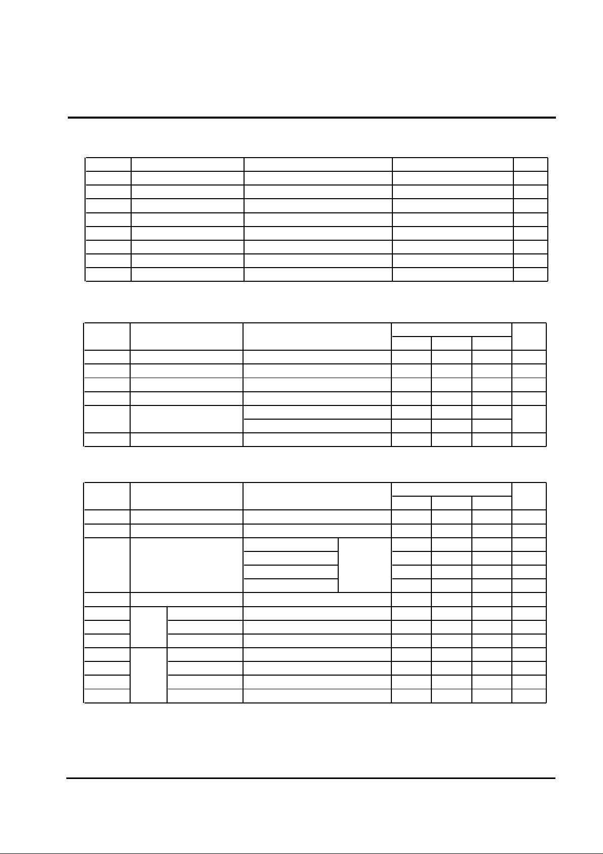
ABSOLUTE MAXIMUM RATINGS (Ta=25°C, unless otherwise noted)
Symbol Parameter Conditions Ratings Unit
Vcc Supply voltage V
ISINK1,2 Output Sink Current Output1,2 8.0 mA
VO Output voltage V
VRES V
Self reset input voltage
Pd Power dissipation 300 mW
Ktheta Thermal Derating 3.0 mW/°C
Ta ≥ 25°C
Topr Operating temperature
Tstg Storage temperature
ELECTRICAL CHARACTERISTICS (Ta = -20 to 75°C, unless otherwise noted)
< Reset circuit 1 >
Symbol Parameter Test Conditions
VS1 Detecting voltage 1 Ta= 25°C 1.20 1.25 1.30 V
∆Vs1
TPLH1 CL=100pF,Ta= 25°C 80 200 500
VOL1 VIN<1.2V, IOL=5mA, Vcc=5V 0.2 0.4 V
VIN
Hysteresis voltage 1
Output "L to H" propagation delay time 1
Low output voltage 1
Input voltage
Ta= 25°C 9 15 23 mV
Vcc ≤ 7V
Vcc > 7V
IIN Input Current VIN=1.25V 100 500 nA
-0.3 to 10
-0.3 to 10
-0.3 to 10
-20 to 75 °C
-40 to 125
Limits
Min Typ Max
-0.3 Vcc
-0.3 7.0
°C
Unit
µs
V
< Reset circuit 2 >
Symbol Parameter Test Conditions
S2 Detecting voltage 2
V
Ta= 25°C 4.0 4.2 4.4 V
Min Typ Max
Limits
Unit
∆ VS2 Hysteresis voltage 2 Ta= 25°C 30 50 100 mV
Ct0 ="L", Ct1="H"
T
PLH2
VOL2
VRESH Input High voltage 2 Vcc V
IRESH Input High current VRES=2V 80
Output "L to H" propagation delay time 2
Low output voltage 2
Self
Reset
VRESL Input Low voltage -0.3 0.8 V
VCt0,1H Input High voltage 1.4 V
VCt0,1L Input Low voltage 0.6 V
ICt0,1H Input High current 75
Ct0
Ct1
ICt0,1L Input Low current 75
Ct0 ="H", Ct1="L"
Ct0 ="H", Ct1="H" or opening
Ct0="L",Ct1="L"
CL=100pF 50 ms
Ta= 25°C 100 ms
Vcc=4.0V,IOL=5mA 0.2 0.4 V
Ta= 25°C
Ta= 25°C
Ta= 25°C
Ta= 25°C
Ta= 25°C
Ta= 25°C
Ta= 25°C
25 ms
200 ms
µA
µA
µA
2
( / 5 )
Page 3

MITSUBISHI<Dig./Ana. INTERFACE>
M62030FP
VOLTAGE DETECTING, SYSTEM RESETTING IC SERIES
ELECTRICAL CHARACTERISTICS (Ta = -20 to 75°C,unless otherwise noted)
< Common specification >
Symbol Parameter Test Conditions Unit
Vcc
Supply Voltage
Min Typ Max
Icc1 Circuit Current in OFF Vcc=5V 1.0 2.0 mA
Icc2
Vs/∆T
∆Vs/∆T
TPLH/∆T 0.10 %/°C
VOH
TPHL CL = 100pF 10
VOPL
R 5 10 15 kΩ
Circuit Current in ON
Detecting Voltage Temperature Coefficient 0.01 %/°C
The hysteresis voltage temperature coefficient
Propagation delay time temperature coefficient
Output High Voltage
Output "H to L" propagation delay time
*1
Threshold Operating Voltage
Built-in pull-up resistor
Both circuit "ON" state. Contain pull-up resistor
IOH = -40µA Vcc-0.6 Vcc-0.4 Vcc-0.2
Ta = 25°C 0.67
Note*1: Minimum supply voltage to keep output low
Limits
2 10 V
2.0 4.0 mA
0.01 %/°C
0.8
V
µs
V
PIN DESCRIPTION
Terminal No. Symbol Functional Description
1
3
Ct0
Ct1
2 VIN
4 GND
6 OUT1
5 OUT2
7 Vcc
8 VRES
Setting delay time.
It is possible to set 4 kinds of delay
times by inputting "H" or "L" into
these two terminal.
Detecting voltage input
Ground
Output terminal 1 (Delay time 200µs settlement output)
Output terminal 2 (Delay time variable type output)
Supply voltage
It outputs "L"and "H" to OUT2 terminal when the VRES input is "H" and "L", respectively.
Ct0 L H H L
Ct1 H L H L
25ms 50ms 100ms 200ms
3
( / 5 )
Page 4

FUNCTION DIAGRAM
In this case, a detection power supply voltage is approximately 1.25 x (R1+R2)/ R2 (v).
The detecting supply voltage can be set between 2V and 10V.
Note 2. The detecting voltage can be adjusted by changing R1 and/or R2 in the following circuit.
The detection accuracy is ±4%.
Note 3. It has a delay capacitor and the delay time is about 200µs.
2
8
VIN
VRES
1
3 4
5
6
OUT2
OUT1
Ct0 Ct1 GND
7
Vcc
M62030FP
SUPPLY
VOLTAGE
GND
MCU
R1
R2
RESET(RESET)
Vcc
OUTPUT 2
H
L
H
L
4
MITSUBISHI<Dig./Ana. INTERFACE>
M62030FP
VOLTAGE DETECTING, SYSTEM RESETTING IC SERIES
INPUT
VOLTAGE
1.25V
SUPPLY
VOLTAGE
4.20V
t t
OUTPUT 1
TPLH1
Input voltage detecting type
t
Supply voltage detecting type
TPLH2
t
EXAMPLE OF APPLICATION CIRCUIT
1) The application to microprocessor system
Note 1. The Input voltage detection type can be used as the voltage supervisor of microprocessor system
like the following circuit.
( / 5 )
Page 5

MITSUBISHI<Dig./Ana. INTERFACE>
M62030FP
VOLTAGE DETECTING, SYSTEM RESETTING IC SERIES
2) The Variable setup time type
Note 1. A delay time of the supply voltage detection type can be set to one among 25ms, 50ms, 100ms and
200ms by the combination of pin 1 and pin 3.
Vcc
SUPPLY
R1
R2
VIN
2
M62030FP
VRES
8
Ct0 Ct1 GND
1 3
7
Vcc
OUT2
OUT1
5
6
4
The other system reset
VOLTAGE
RESET(RESET)
MCU
GND
!
Mitsubishi Electric Corporation puts the maximum effort into making semiconductor products better and more reliable, but
there is always the possibility that trouble may occur with them. Trouble with semiconductors may lead to personal injury,
fire or property damage. Remember to give due consideration to safety when making your circuit design,in order to prevent
fires from spreading, redundancy, malfunction or other mishap.
5
( / 5 )
 Loading...