

Page 1
MITSUBISHI<Dig.Ana.INTERFACE>
components.
power supply and battery.
1
M62021L,P,FP
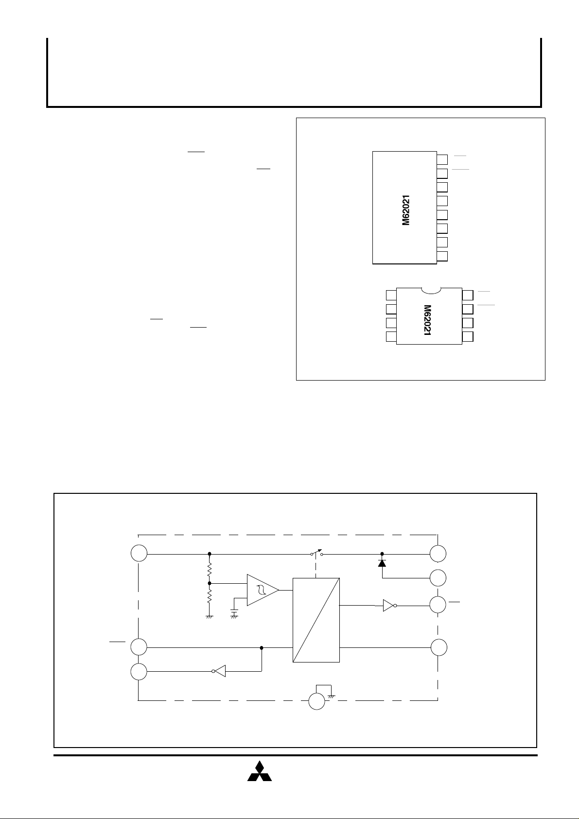
SYSTEM RESET IC WITH SWITCH FOR MEMORY BACK-UP
DESCRIPTION
The M62021 is a system IC that controls the memory backup
function of SRAM and microcomputer (internal RAM).
The IC outputs reset signals(RES/RES) to a microcomputer
at power-down and power failure.It also shifts the power
supply to RAM from main to backup,outputs a signal (CS) that
invokes standby mode,and alters RAM to backup circuit mode.
The M62021 contains,in a single chip,power supply monitor
and RAM backup functions needed for a microcomputer
system,so that the IC makes it possible to construct a system
easily and with fewer components compared with a
conventional case that uses individual ICs and discrete
FEATURES
•Built-in switch for selection between main power supply and
backup power supply to RAM.
•Small difference between input and output voltage
(IOUT=80mA,VIN=5V)0.2V typ
•Detection voltage (power supply monitor voltage)4.40V±0.2V
•Chip select signal output(CS)
Two channels of reset outputs(RES/RES)
•Power on reset circuit built-in
•Delay time variable by an external capacitance connected to
Ct pin
•Facilitates to form backup function with a few number of
components
APPLICATION
Power supply control systems for memory backup of
microcomputer system and SRAM boards with built-in
backup function that require switching between external
PIN CONFIGURATION (TOP VIEW)
8
CS
7
RES
6
GND
5
RES
4
Ct(DELAY CAPACITANCE)
3
VIN
2
VBAT
1
VOUT
Outline 8P5(L)
VBAT
VIN
1
2
3
4
Outline 8P4(P)
8P2S-A(FP)
VOUT
Ct(DELAY CAPACITANCE)
8
CS
7
RES
6
GND
5
RES
BLOCK DIAGRAM
VIN
3
RES
7
RES
5
R1
R2
+
1.24V
Com
RESET
CIRCUIT
MITSUBISHI
ELECTRIC
SW
DELAY
CIRCUIT
6
GND
D1
2
8
4
VOUT
VBAT
CS
Ct
1
( / 9 )
Page 2
MITSUBISHI<Dig.Ana.INTERFACE>
M62021L,P,FP
SYSTEM RESET IC WITH SWITCH FOR MEMORY BACK-UP
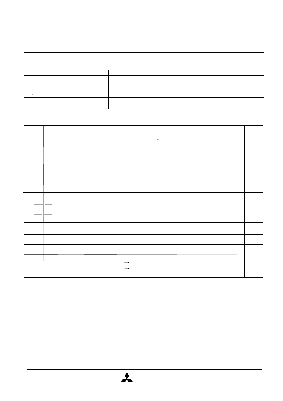
ABSOLUTE MAXIMUM RATINGS(Ta=25°C, unless otherwise noted)
Symbol Ratings
VIN
IOUT
Pd
K
Topr
Tstg Storage temperature
Input voltage
Output current
Power dissipation
Thermal derating
Operating temperature
Parameter
(Ta≥25°C)
ELECTRICAL CHARACTERISTICS(Ta=25°C, unless otherwise noted)
Symbol
Vs
Detection voltage
∆Vs
Hysteresis voltage
Vs/∆T
VDROP
VOH(Ct)
VOL(Ct)
VOH(RES)
VOH(RES)
VOL(RES)
VOH(CS)
VOL(CS)
VOPL(RES)
Note 1.Regarding conditions to measure VOH and VOL,voltage values are to be generated by internal resistance only and no external resistor is used.
2.These values are produced inserting an external resistor,RCS=1MΩ,between the CS pin and GND.
3.With no external resistor (10kΩ internal resistance only)
Temperature coefficient of detection voltage
Circuit current
ICC
Difference between input and output voltage
Ct output voltage (high level)
Ct output voltage (low level)
RES output voltage (high level)
RES output voltage (low level)VOL(RES)
RES output voltage (high level)
RES output voltage (low level)
CS output voltage (high level)
CS output voltage (low level) VIN=5V
Backup Di leak current
IR
VF
Backup Di forward direction voltage
tpd
Delay time
Response time
td
RES limit voltage of operation
Parameter
VIN(At the change from H L)
∆Vs=VSH-VSL
IOUT=0mA
VIN=5V
VIN=5V(Note1)
VIN=4V(Note1)
VIN=4V(Note1)
VIN=5V
VIN=5V(Note1)
VIN=4V
(Note2)
VIN=4V
VIN=0V,VBAT=3V
VBAT=3V
IF=10µA
VIN=0V
VIN=5V
(Note 3)
Conditions
Test conditions
(Note2)
5V,Ct=4.7µF
4V
VIN=4V
VIN=5V
IOUT=50mA
IOUT=80mA
(Note1)
ISINK=1mA
(Note1)
ISINK=1mA
(Note1)
ISINK=1mA
VIN=5V
VIN=0V
7
100
800(SIP)/625(DIP)/440(FP)
8(SIP)/6.25(DIP)/4.4(FP)
-20 ~ +75
-40 ~ +125
Limits
Min.
4.2
50 200
4.5
3.5
4.5
3.50
2.40
10
Typ.
4.4
2.0
7.5
0.125
0.2
5.0
0.02
4.0
0.02
0.05
5.0
0.02
0.05
3.57
2.47
0.08
0.1
0.54
27
5.0
0.65
Max.
4.6
4.0
12.0
0.25
0.4
0.1
0.2
0.2
0.3
±0.5
±0.5
0.6
55
25.0
Unit
V
mA
mW
mW/°C
°C
°C
Unit
V
mV100
%/°C0.005
mA
V
V
V
V
V
V
V
V
V
µA
V
ms
µs
V
MITSUBISHI
ELECTRIC
2
( / 9 )
Page 3
1.24VR1R2
D1
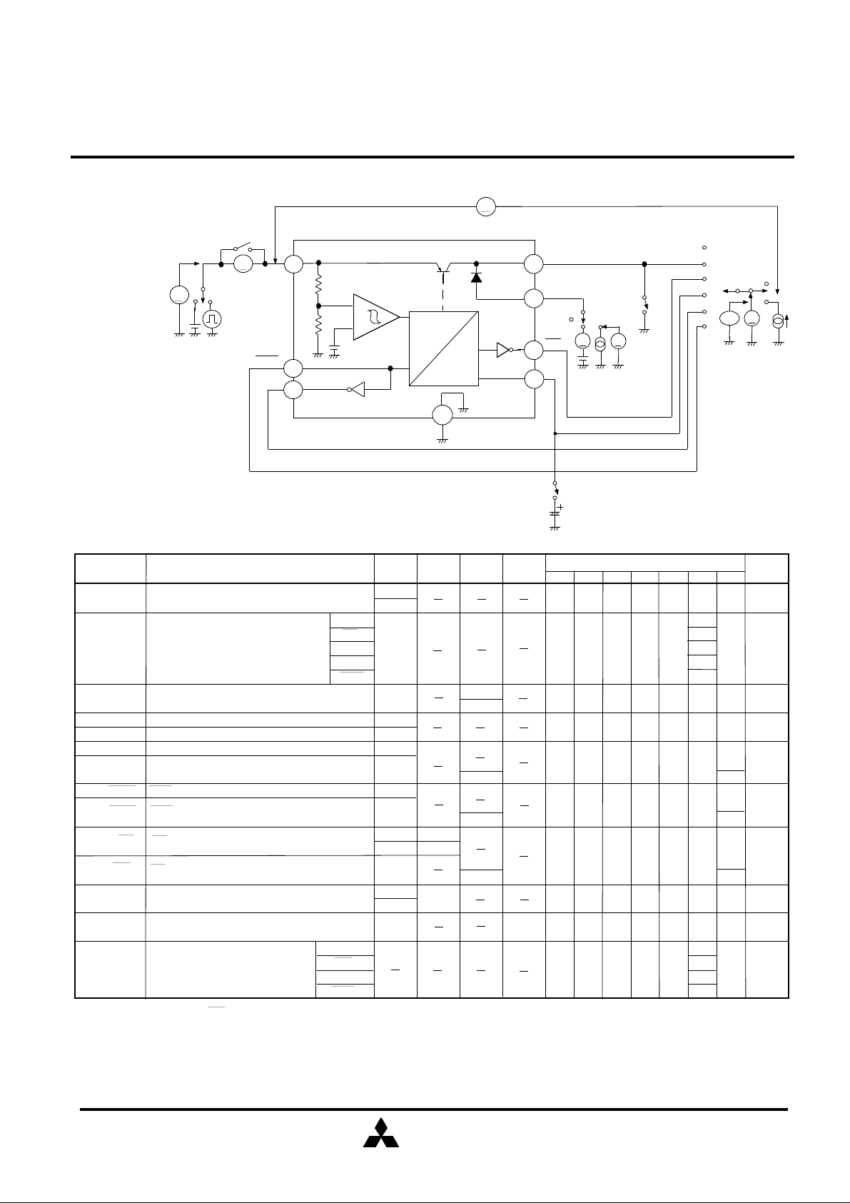
TEST CIRCUIT
CRT1234
56SW5
SW6
SW712
IF1
Vm4
SW4
SW3
4.7µ
Vm3
IF2
V2
Im2123Vm2
VIN
SW2
Im1
Measuring
instrument
(Note6)
(Note7)
SW112
V1
MITSUBISHI<Dig.Ana.INTERFACE>
M62021L,P,FP
SYSTEM RESET IC WITH SWITCH FOR MEMORY BACK-UP
V
M62021
1
2
8
4
VOUT
VBAT
CS
Ct
V
A
V
Vm1
A
V
RES
RES
3
Com
+
-
7
RESET
CIRCUIT
DELAY
CIRCUIT
5
6
GND
SWITCH MATRIX
ON
ON
ON
ON
ON
ON
ON
ON
ON
ON
S W
OFF
OFF
OFF
OFF
OFF
OFF
OFF
OFF
OFF
ON
7
1
OFF
1
1
OFF
1
OFF
OFF
1
1
OFF
1
2
3
4
5
6
2
4
5
1
2
1
1
(Note5)
Vm4
CRT
Vm1
2
1
OFF
1
6
2
OFF
1
1
3
2
2
3
OFF
ON
1
1
1
1
2
OFF
3
1
5
1
6
Symbol
Icc
Parameter
Circuit current
V1 V2 IF1
4V
5V
IF2
1 2 3 4 5 6
1
VOUT
Decrease
Vs
(VSL)
Detection voltage
(VIN negative-going)
CS
Ct
RES
from
5V
1
RES
3V
3V
-50mA
-80mA
1mA
1mA
1mA
10µA
1
1
1
1
1
1
1
2
VDROP
VOH(Ct)
VOL(Ct)
VOH(RES)
VOL(RES)
VOH(RES)
VOL(RES)
VOH(CS)
VOL(CS)
IR
VF
tpd
td
Difference between input and output voltage
Ct output voltage(high level)
Ct output voltage(low level)
RES output voltage(high level)
RES output voltage(low level)
RES output voltage(high level)
RES output voltage(low level)
CS output voltage(high level)(Note 4)
CS output voltage(low level)
Backup Di leak current
Backup Di forward direction voltage
Delay time
Response time
VOUT
CS
RES
5V
5V
4V
4V
5V
5V
4V
4V
0V
5V
5V
0V
0V
RES
Notes 4.To measure VOH(CS),insert a 1MΩ resistor between the CS pin and GND.
5. While monitoring each output by Vm4 or CRT,measure the input voltage Vm1 when the output goes from H to L and L to H.Regarding VSH,raise VIN
from 4V and measure the input voltage Vm1 when the output goes from H to L and L to H.∆Vs is VSH-VSL.
6. To measure delay time, change VIN from 0V to 5V and compare,with respect to each pin,the positive-going edge observed on a monitor with that
of VIN.To measure response time,change VIN from 5V to 4V and compare,with respect to each pin,the negative-going edge observed on a monitor
with that of VIN.
7.Set the switch to OFF when measuring response time.
Im1
Vm2
Vm4
Vm4
Vm4
Vm4
Im2
Vm3
CRT
MITSUBISHI
ELECTRIC
( / 9 )
3
Page 4

4
EXPLANATION OF TERMINALS
MITSUBISHI<Dig.Ana.INTERFACE>
M62021L,P,FP
SYSTEM RESET IC WITH SWITCH FOR MEMORY BACK-UP
Pin No.
1
2 VBAT
3
4
5
6
7
8
Symbol Name
VOUT
VIN
Ct Delay capacitor connection pin
RES
GND
RES
CS
Power supply output
Backup power supply input
Power supply input
Positive reset output
Ground
Negative reset output
Chip select output
APPLICATION EXAMPLE
Function
VIN and VBAT are controlled by means of an internal switch and output
through VOUT
The pin is capable of outputting up to 100mA.Use it as VDD of CMOS RAM
and the like
Backup power supply is connected to this pin
If a lithium battery is used,insert a resistor in series for safety purposes
+5V input pin.Connect to a logic power supply.
A delay capacitor is connected to this pin.By connecting a capacitor,it is
possible to delay each output
Connect to the positive reset input of a microcomputer.The pin is capable
of flowing 1mA sink current
Reference for all signals
Connect to the negative reset input of a microcomputer.The pin is capable
of flowing 1mA sink current
Connect to the chip select of RAM.The CS output is at low level in normal
state thereby letting RAM be active.Under failure or backup condition,the CS
output is set to high level,then RAM enters standby state disabling read/write
function.The pin is capable of flowing a 1mA sink current
+5V
(MAIN POWER SUPPLY)
CIN
VDD
CPU
VIN
RES
RES
M62021
VOUT
D1
1
2
8
4
VBAT
CS
Ct
3
R1
Com
+
R2
-
1.24V
7
5
RESET
CIRCUIT
DELAY
CIRCUIT
6
GND
*Capacitance to be connected:CIN:10µF;COUT:4.7µF;Ct:4.7µF
*If connecting a zener diode,select one of VZ=2~3V
VIN
BATTERY
3V
VDD
CONT
CMOS
RAM
MITSUBISHI
ELECTRIC
( / 9 )
Page 5

SYSTEM RESET IC WITH SWITCH FOR MEMORY BACK-UP
that the input voltage slowly drops or VR nearly equals Vref.
Delay time is determined as follows.
3
supply,avoid connecting a too large capacitance.
chattering.
CONFIGURATION
<Power supply detector>
The internal reference voltage Vref is compared by means of
a comparator with resistor-divided voltage VR(resistor-divided
voltage produced by R1 and R2 from VIN).
If the input voltage is 5V,VR is set to 1.24V or higher,so the
comparator output is at low level and the Ct output(Q1
collector output)is set to high level.If the input voltage drops to
below 4.4V in an abnormal condition,VR becomes below
1.24V,so the comparator output goes from low to high level
and the Ct output,from high to low.The input voltage at this
point is called VSL.Next,when the input voltage,restored from
abnormal state,has a rise,the comparator output goes from
high to low level and the Ct output,from low to high.
The comparator used for detection has 100mV
hysteresis(∆Vs),so that malfunctioning is prevented in case
MITSUBISHI<Dig.Ana.INTERFACE>
M62021L,P,FP
5
4
3
2
1
0
4.0
VSL VSH
4.2
∆Vs
4.4 4.6 4.8
5.0
<Delay Circuit>
Connecting an external capacitor to the Ct pin lets
RES,RES,CS,and VOUT be delayed due to RC transient
phenomenon(electric charge).
Delay time(tpd)= Ct X (R3 + R4) X In
=Ct X 22kΩ X 0.2614
.
=5.75 X 10 X Ct *Ct is an external capacitance.
.
Taking into consideration the time taken by the oscillator of
microcomputer to be stable,connect a 4.7µF capacitor to the
Ct pin.
(As the response time of detection can be slowed due to
internal structure depending on the rising rate of power
<Schmitt trigger circuit>
Since waveforms show a gentle rise due to the RC delay
circuit,INV1,INV2,R5,and R6 constitute a schmitt trigger circuit
to produce hysteresis so as to prevent each output from
[VOH(Ct)-VOL(Ct)]
[VOH(Ct)-INV1(VTH)]
INTERNAL CIRCUIT
Ct
4
R2
24K
R1
60.94k
1.24V
Vref
Com
R3
22k
R4 R5
47
Q1
10k
R6
INV1
INV2
VIN
3
INV3 INV4
INV5
INV8
INPUT VOLTAGE VIN(V)
tpd
DELAYED OUTPUT WAVEFORMS OF Ct
RES RES
R8
R7
10k 10k
Q2
Q3
INV7
INV6
R9
5k
INV9
R10
22k
75
R10
800
Q4
Q5
VOH(Ct)
INV1(Vth)
VOL(Ct)
R11
10k
D1
1
2
8
6
VOUT
VBAT
CS
GND
MITSUBISHI
ELECTRIC
( / 9 )
5
Page 6

The output is a logic high
and the output level is
VBAT-VF
TIMING CHART
MITSUBISHI<Dig.Ana.INTERFACE>
M62021L,P,FP
SYSTEM RESET IC WITH SWITCH FOR MEMORY BACK-UP
VIN
0V
VOUT
CS
RES
5V
tpd
tpd
∆Vs
VSH
VSL
V1
V2
V3
V4
V5
V2
V4
V5
VOL(CS)
5V
VIN(VSL)
VOL(RES)
VOL(RES)
VIN(VSL)
Input
voltage
Output
pin
VOUT
RES
RES
CS
RES
In normal operation
Input voltage:5V
With Q4 set to ON,
a voltage
(VIN-VDROP)is output
The output level is
VOL(RES)
with a logic low
The output level is
VOH(RES)
with a logic low
The output level is
VOL(CS)
with a logic low
In failure(instantaneous drop)
Input voltage:5V 4V
Each output varies if the input
voltage drops to VSL or under
Q4 is turned OFF.A voltage
(VIN-Q4 VEB(Di) is output by
the diode between E and B of
Q4
As the state shifts from a logic
low to logic high,the output level
becomes approximately equal to
the input voltage
As the state shifts from a logic
high to logic low,the output level
becomes VOL(RES)
As the state shifts from a logic
low to logic high,the output level
becomes the voltage VINQ4EB(Di).
V1=VIN-VDROP
V2=VIN-Q4VEB(Di)
V3=VIN(VSL)-VDROP
V4=VIN(VSL)-Q4VEB(Di)
V5=VBAT-VF
Restoration from failure
(instantaneous drop)
Input voltage:4V 5V
If the input voltage goes higher
than VSL by 100mV,each out-put
varies after delay produced by the
delay circuit
Q4 is turned ON after delay and
a voltage(VIN-VDROP) is output
A logic high is maintained,and than
shifts to a logic high
A logic low is held,and than shifts
to a logic high
A logic high is maintained,and than
shifts to a logic high
VOL(RES)
In backup state
Input voltage:0V
Backup voltage:3V
VBAT-VF
MITSUBISHI
ELECTRIC
( / 9 )
6
Page 7

SYSTEM RESET IC WITH SWITCH FOR MEMORY BACK-UP
TYPICAL CHARACTERISTICS
MITSUBISHI<Dig.Ana.INTERFACE>
M62021L,P,FP
1000
800
600
400
200
4.48
4.46
4.44
4.42
4.40
4.38
4.36
4.34
4.32
THERMAL DERATING
(MAXIMUM RATING)
M62021L
M62021P
M62021FP
0
0
25
50
75
AMBIENT TEMPERATURE Ta(°C)
DETECTION VOLTAGE VS.
AMBIENT TEMPERATURE
-20
-40
0 20 40 80
AMBIENT TEMPERATURE Ta(°C)
60
100
100
125
120
CIRCUIT CURRENT VS.
INPUT VOLTAGE
16
14
12
10
8
6
4
2
0
0 1 2 3
INPUT VOLTAGE Vcc(V)
INTERRUPTION OUTPUT VOLTAGE VS.
140
130
120
110
100
90
80
70
60
-40
SUPPLY VOLTAGE
-20
0 20 40 80
AMBIENT TEMPERATURE Ta(°C)
4
5 6 7 8
60
100
120
CIRCUIT CURRENT VS.
10
9
8
7
6
5
4
3
2
-40
AMBIENT TEMPERATURE
VIN=5V
-20
0 20 40 80
AMBIENT TEMPERATURE Ta(°C)
60
100
120
MITSUBISHI
ELECTRIC
CIRCUIT CURRENT VS.
4.0
3.5
3.0
2.5
2.0
1.5
1.0
0.5
AMBIENT TEMPERATURE
VIN=4V
0
-20
-40
0 20 40 80
AMBIENT TEMPERATURE Ta(°C)
60
100
120
( / 9 )
7
Page 8

MITSUBISHI<Dig.Ana.INTERFACE>
8
M62021L,P,FP
SYSTEM RESET IC WITH SWITCH FOR MEMORY BACK-UP
DIFFERENCE BETWEEN INPUT AND OUTPUT
100
80
60
40
20
0
160
140
120
100
80
60
40
OUTPUT CURRENT VS.
VOLTAGES
VIN=5V
0
DIFFERENCE BETWEEN INPUT
AND OUTPUT VOLTAGES VDROP(mV)
BACKUP Di FORWARD DIRECTION
CURRENT VS. VOLTAGE
50
100
150 200
250
DIFFERENCE BETWEEN INPUT AND OUTPUT
400
350
300
250
IOUT=100mA
200
IOUT=80mA
150
IOUT=50mA
100
50
0
-40
AMBIENT TEMPERATURE Ta(°C)
BACKUP Di FORWARD DIRECTION
VOLTAGE VS. AMBIENT TEMPERATURE
0.8
0.7
0.6
0.5
0.4
0.3
0.2
VOLTAGES VS.
AMBIENT TEMPERATURE
VIN=5V
-20
20
0
40
60 80
100
IF=100µA
IF=10µA
IF=1µA
120
20
0
0
0.2 0.3 0.4 0.5 0.6 0.7
0.1
BACKUP Di FORWARD DIRECTION VOLTAGE VF(V)
RES"L"OUTPUT VOLTAGE VS.
80
70
60
50
40
30
20
10
0
AMBIENT TEMPERATURE
VIN=5V
ISINK=1mA
-40
-20
AMBIENT TEMPERATURE Ta(°C)
20
0
40
60 80
100
0.8
120
0.1
0
-40
-20
AMBIENT TEMPERATURE Ta(°C)
RES "L"OUTPUT VOLTAGE VS.
80
VIN=4V
70
ISINK=1mA
60
50
40
30
20
10
0
-40
-20
AMBIENT TEMPERATURE Ta(°C)
20
20
40
40
0
AMBIENT TEMPERATURE
0
60 80
60 80
100 120
100 120
MITSUBISHI
ELECTRIC
( / 9 )
Page 9

MITSUBISHI<Dig.Ana.INTERFACE>
23752375237523752375237
5
M62021L,P,FP
SYSTEM RESET IC WITH SWITCH FOR MEMORY BACK-UP
CS"L"OUTPUT VOLTAGE VS.
160
140
120
100
80
60
40
20
1000
100
AMBIENT TEMPERATURE
VIN=5V
ISINK=1mA
0
-40
-20
AMBIENT TEMPERATURE Ta(°C)
DELAY TIME VS.EXTERNAL CAPACITANCE
VIN=0V 5V
20
0
CONNECTED TO THE Ct PIN
40
60 80
100 120
CS"L"OUTPUT VOLTAGE VS.
4.0
3.8
3.6
3.4
3.2
3.0
2.8
2.6
2.4
40
35
30
25
AMBIENT TEMPERATURE
VIN=4V
RCS=1MΩ
-40
-20
AMBIENT TEMPERATURE Ta(°C)
DELAY TIME VS.AMBIENT
VIN=0V 5V
Ct=4.7µA
20
0
40
TEMPERATURE
60 80
100
120
10
0
0.1
EXTERNAL CAPACITANCE CONNECTED
1 10 100
TO THE Ct PIN Ct(µF)
20
15
10
5
0
-40
-20
AMBIENT TEMPERATURE Ta(°C)
20
0
40
60 80
100 120
MITSUBISHI
ELECTRIC
( / 9 )
9
 Loading...