

Page 1
3V Supply Low Pin Count Flash Memory
■ SUPPLY VOLTAGE
= 3V to 3.6V for Program, Erase and
–V
CC
Read Operations
–V
= 12V for Fast Program and Fast Erase
PP
■ LOW PIN COUNT (LPC)
– Standard Interface for embedded operation
with PC Chipsets that are without automapping memory features
■ ADDRESS/ADDRESS MULTIPLEXED
– A/A Mux Interface for programming equip-
ment compatibility
■ LOW PIN COUNT (LPC) HARDWARE
INTERFACE MODE
– 5 Signal Communication Interface supporting
Read and Write Operations
– Hardware Write Protect Pins for Block Pro-
tection
– Register Based Read and Write Protection
– 5 Additional Ge neral Purp ose I nputs f or pla t-
form design flexibility
– Synchronized with 33MHz PCI clock
■ BYTE PROGRAMMING TIME
– Single Byte Mode: 10µs (typical)
– Quadruple Byte Mode: 2.5µs (typical)
■ 8 UNIFORM 64 Kbyte MEMORY BLOCKS
■ PROGRAM/ERA SE CON TROLLER
– Embedded Byte Program and Block/Chip
Erase algorithms
– Status Register Bits
■ PROGRAM and ERASE SUSPEND
– Read other Blocks during Program/Erase
Suspend
– Program other Blocks during Erase Suspend
■ FOR USE in PC BIOS APPLICATIONS
■ ELECTRONIC SIGNATURE
– Manufacturer Code: 20h
– Device Code: 3Ch
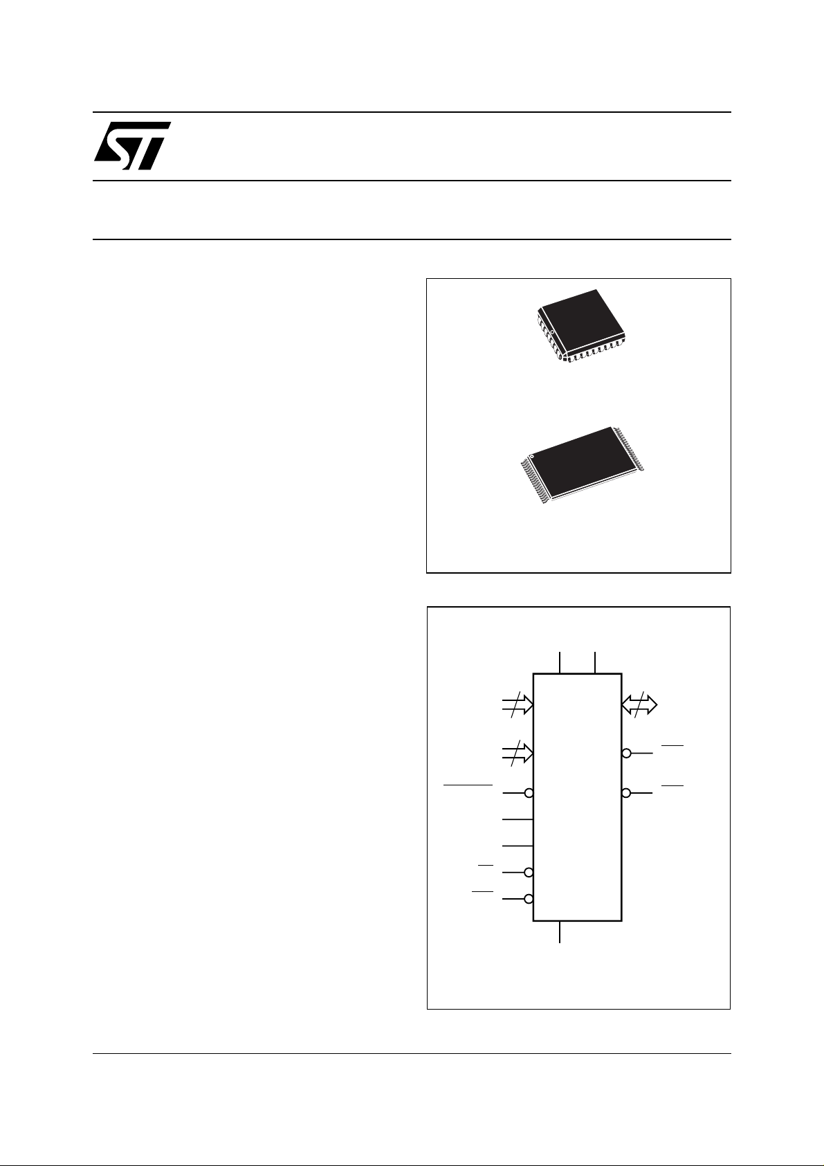
M50LPW041
4 Mbit (512Kb x8, Un iform B lock )
PRELIMINARY DATA
PLCC32 (K)
TSOP40 (N)
10 x 20mm
Figure 1. Logic Diagram (LPC Interface)
V
ID0-ID3
GPI0-
GPI4
LFRAME
CLK
IC
RP
INIT
V
4
5
M50LPW041
V
CC
SS
PP
4
LAD0LAD3
WP
TBL
AI05785
September 2002
This is preliminary information on a new product now in development or undergoing evaluation. Details are subject to change without notice.
1/37
Page 2
M50LPW041
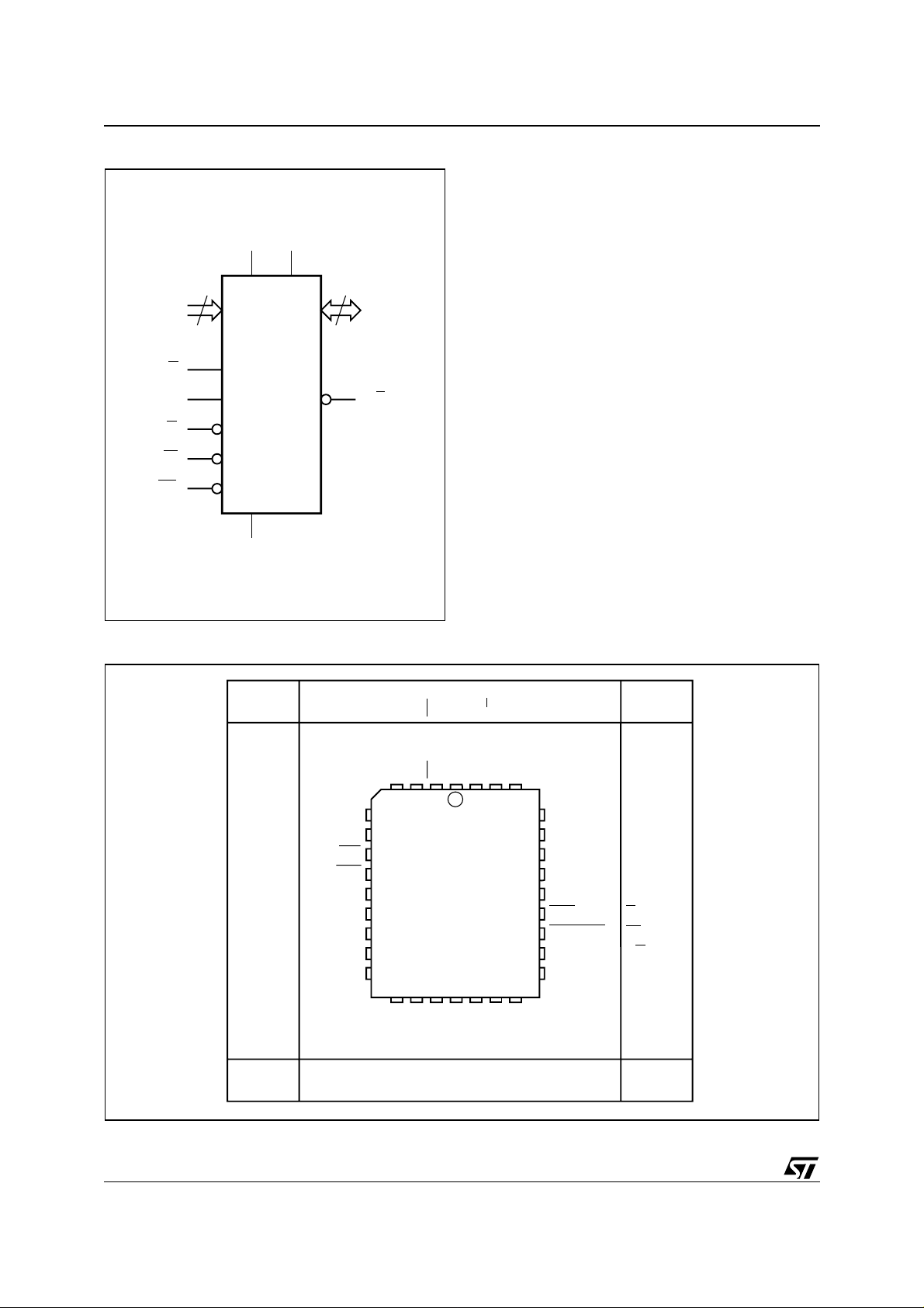
Figure 2. Logic Diagram (A/A Mux Interface)
V
A0-A10
RC
IC
W
RP
V
11
M50LPW041
G
V
CC
SS
PP
8
DQ0-DQ7
RB
AI05786
DESCRIPTION
The M50LPW041 is a 4 Mbit (512Kb x8) nonvolatile memory that can be read, erased and
reprogrammed. These operations can be
performed using a single low voltage (3.0 to 3.6V)
supply. For fast pro gramming and fast erasing in
production lines an optional 12V power supply can
be used to reduce the programming and the
erasing times.
The memory is divided into blocks that can be
erased independently so it is pos sible to pres erve
valid data while old data is erased. Blocks can be
protected individually to prevent accidental
Program or Erase commands from modifying the
memory. Program and Erase commands are
written to the Command Interface of the m emory.
An on-chip Program/Erase Controller simplifies
the process of programming or erasing the
memory by taking care of all of the special
operations that are required to update the memory
contents. The end of a program or erase operation
can be detected and any error conditions
identified. The command set required to control
the memory is consistent with JEDEC standards.
Two different bus interfaces are supported by t he
memory. The primary interface is the Low Pin
Count (or LPC) Standard Interface. This has been
Figure 3. PLCC Connections
A/A Mux A/A Mux
A7
A6
A5
A4
A3
A2
A1
A0
DQ0
Note: Pins 27 and 28 are not internally connected.
GPI1
GPI0
WP
TBL
ID3
ID2
ID1
ID0
LAD0
GPI2
9
LAD1
DQ1
RPA8VPPV
A9
RP
VPPV
GPI3
1
32
M50LPW041
17
SS
V
V
SS
RFU
LAD3
DQ3
DQ4
LAD2
DQ2
CC
CC
RC
CLK
RFU
DQ5
A10
GPI4
25
RFU
DQ6
IC (VIL)
NC
NC
V
SS
V
CC
INIT
LFRAME
RFU
RFU
IC (VIH)
NC
NC
V
SS
V
CC
G
W
RB
DQ7
A/A MuxA/A Mux
AI05788
2/37
Page 3
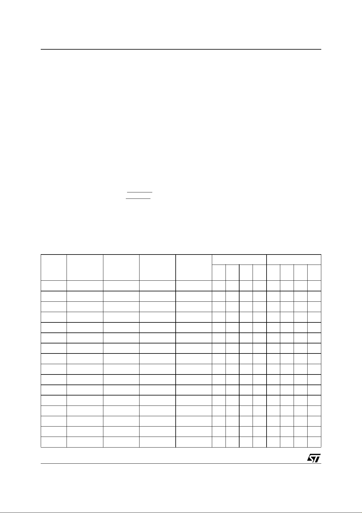
Figure 4. TSOP Connections
M50LPW041
NC
IC (VIH)
NC
NC
NC
NC
A10
NC
RC
V
CC
V
PP
A/A Mux
RP
NC
NC
A9
A8
A7
A6
A5
A4 A3
NC
IC (VIL)
NC
NC INIT
NC RFU
NC
GPI4
NC
CLK
V
CC
V
PP
RP
NC
NC
GPI3
GPI2 LAD0
GPI1 ID0
GPI0
WP
TBL
1
10
M50LPW041
11
20 21
40
31
30
V
V
LFRAME
RFU
RFU
RFU
RFU
V
V
V
LAD3
LAD2
LAD1
ID1
ID2
ID3
SS
CC
CC
SS
SS
V
SS
V
CC
W
G
RB
DQ7
DQ6
DQ5
DQ4
V
CC
V
SS
V
SS
DQ3
DQ2
DQ1
DQ0
A0
A1
A2
A/A Mux
AI06872
designed to remove the need for the ISA bus in
current PC Chipsets; the M50LPW041 acts as the
PC BIOS on the Low P in Count bus for these P C
Chipsets.
The secondary interface, the Address/Address
Multiplexed (or A/A Mux) Int erface, is design ed t o
be compatible with current Flash Programmers for
production line programming prior to fitting to a PC
Motherboard.
The memory is offered in a PLCC32 or TSOP40
(10mm x 20mm) package and is supplied with all
the bits erased (set to 1).
System Memory Mapping
The LPC address sequence is 32 bits long. The
M50LPW041 responds to addresses mapped to
the top of the 4 GByte memory space, from
FFFF FFFFh. Address bits A31-A24 must be set
to 1. A23 is set to 1 for array access, and to 0 for
register access.
The M50LPW041 also responds to addresses
mapped to the bottom of the 4 GByte memory
space, from 0000 0000h. Address bits A31-A24
must be set to 0. A23 is set to 0 for array access,
and to 1 for register access.
For A22-A19, see Table 2. A18-A0 are for array
addresses.
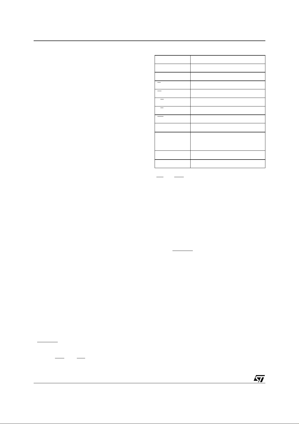
Table 1. Signal Names (LPC Interface) Memory
LAD0-LAD3 Input/Output Communications
LFRAME
ID0-ID3 Identification Inputs
GPI0-GPI4 General Purpose Inputs
IC Interface Configuration
RP
INIT
CLK Clock
TBL
WP
RFU
V
CC
V
PP
V
SS
NC Not Connected Intern ally
Input Communication Frame
Interface Reset
CPU Reset
Top Block Lock
Write Protect
Reserved for Future Use. Leave
disconnected or set at V
Supply Voltage
Optional Supply Voltage for Fast
Erase Operations
Ground
or VIH.
IL
3/37
Page 4
M50LPW041
SIGNAL DESCRIPTIONS
There are two different bus interfaces available on
this part. The active interface is selected before
power-up or during Reset using the Interface Configur a tion Pin, IC.
The signals for each interface are discussed in the
Low Pin Count (LPC) Signal Descriptions section
and the Address/Address M ultiplexed (A/A Mux)
Signal Descriptions section below. The supply signals are discussed in the Supply S ignal Descriptions section below.
Low Pin Count (LPC) Signal Descriptions
For the Low Pin Count (LPC) Interface see Figure
1, Logic Diagram, and Table 1, Signal Names.
Input/Output Communications (LAD0-LAD3). All
Input and Output Communication with the memory
take place on these pi ns. Addresses and Data for
Bus Read and Bus W rite operations are en coded
on these pins.
Input Communication Frame (LFRAME
Input Communication Frame (LFRAME
). The
) signals
the start of a bus operation. When Input Communication Frame is Low, V
, on the rising edge of
IL
the Clock a new bus operat ion is in itiated. If Input
Communication Frame is L ow, V
, during a bus
IL
operation then the operation is aborted. When Input Communication Frame is High, V
, the cur-
IH
rent bus operation is proceeding or the bus is idle.
Identification Inputs (ID0-ID3). The Identification
Inputs (ID0-ID3) allow to address up to 16
memories on a bus. The value on addresses A19A22 is compared to the hardware strapping on the
ID0-ID3 pins to select which memory is being
addressed, as shown in Table 2.
General Purpose Inputs (GPI0-GPI4). The General Purpose Inputs can be used as digital inputs for
the CPU to read. The General Purpose Input Register holds the values on these pins. The pins must
have stable data from before the start of the cycle
that reads the General Purpose Input Register until after the cycle is complete. These pins must not
be left to float, they should be driven Low, V
High, V
.
IH
IL,
or
Interface Configuration (IC). The Interface Configuration input selects whether the Low Pin Count
(LPC) or the Address/Address Multiplexed (A/A
Mux) Interface is used. The chosen interface must
be selected before power-up or during a Reset
and, thereafter, cannot be change d. The state of
the Interface Configuration, IC, should not be
changed during operation.
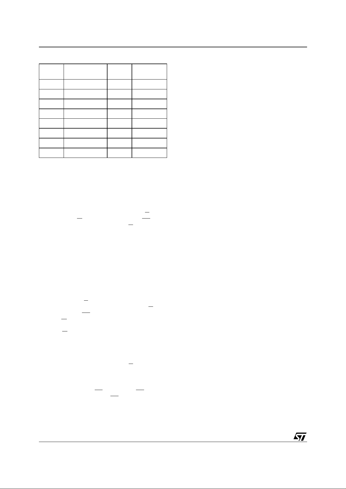
Table 2. Memory Identification Input Configuration
Memory
Number
1 (Boot)
2
3
4
5
6
7
8
9
10
11
12
13
14
15
16
ID2 ID2 ID1 ID0
or floating VIL or floating VIL or floating VIL or floating
V
IL
V
or floating VIL or floating VIL or floating V
IL
V
or floating VIL or floating V
IL
V
or floating VIL or floating V
IL
V
or floating V
IL
V
or floating V
IL
V
or floating V
IL
V
or floating V
IL
V
IH
V
IH
V
IH
V
IH
V
IH
V
IH
V
IH
V
IH
IH
IH
IH
IH
VIL or floating VIL or floating VIL or floating
VIL or floating VIL or floating V
VIL or floating V
VIL or floating V
V
IH
V
IH
V
IH
V
IH
IH
IH
VIL or floating VIL or floating
VIL or floating V
V
IH
V
IH
IH
IH
VIL or floating VIL or floating
VIL or floating V
V
IH
V
IH
VIL or floating
VIL or floating
VIL or floating
VIL or floating
Top Bottom
A 22A 21A 20A 19A 22A 21A 20A
11110001
IH
V
IH
IH
V
IH
IH
V
IH
IH
V
IH
11100000
11010011
11000010
10110101
10100100
10010111
10000110
01111001
01101000
01011011
01001010
00111101
00101100
00011111
00001110
19
4/37
Page 5

M50LPW041
Table 3. System Memory Map
A31:24
Top FFh 1 0
Bottom 00h 0 1
A23
Array Register
To select the Low Pin Count (LPC) Interface the
Interface Configuration pin should be left to float or
driven Low, V
; to select the Address/Address
IL
Multiplexed (A/A Mux) Interface t he pin should be
driven High, V
included with a value of R
current of I
. An internal pull-down resistor is
IH
through each pin when pulled to VIH;
LI2
; there will be a leakage
IL
see Table 21.
Interface Reset (RP
). The Interface Reset (RP)
input is used to reset the memory. When Interface
Reset (RP
) is set Low, VIL, the memor y i s i n R ese t
mode: the outputs are put to high impedance and
the current consumption is minimized. When RP
set High, V
, the memory is in no rmal operat ion.
IH
is
After exiting Reset mode, the memory enters
Read mode.
CPU Reset (INIT
). The CPU Reset, INIT, pin is
used to Reset the memory when the CPU is reset.
It behaves identically to Interface Reset, RP
, and
the internal Reset lin e is the logical OR (elec tric al
AND) of RP
and INIT.
Clock (CLK). The Clock, CLK, input is used to
clock the signals in and out of the Input/Output
Communication Pins, LAD0-LAD3. The Clock
conforms to the PCI specification.
Top Block Lock (TB L
). The Top Block Lock
input is used to pre vent the Top Block (Block 7)
from being chan ged. When Top Block Loc k, TBL
is set Low, V
, Program and Block Erase
IL
operations in the Top Block have no effect,
regardless of the state of the Lock Register. When
Top Block Lock, TBL
, is set High, VIH, the
protection of the Block is determined by the Lock
Register. The state of Top Block Lock, TBL
, does
not affect the protection of the Main Blocks (Blocks
0 to 6).
Top Block Lock, TBL
, must be set prior to a Program or Block Erase operation is initiated and
must not be changed until the operation completes
or unpredictable results may occur. Care should
be taken to avoid unpredictable behavior by
changing TBL
Write Protect (WP
during Program or Erase Suspend.
). The Write Protect input is
used to prevent the Main Blocks (Blocks 0 to 6)
from being changed. W hen Write P rotect, WP
set Low, V
, Program and Block Erase operations
IL
, is
in the Main Blocks have no effect, regardless of
the state of the Lock Register. When Write Protect,
, is se t H i g h , VIH, the protection of the Block is
WP
determined by the Lock Register. The state of
Write Protect, WP
, does not affect the protection of
the Top Block (Block 7).
Write Protect, WP
, must be set prior to a Program
or Block Erase operation is initiated and must not
be changed until the o peration completes or unpredictable results may occur. Care should be taken to avoid unpredictable behavior by changing
WP
during Program or Erase Suspend.
Reserved for Future Use (RFU). These pins do
not have assigned func t ions i n this revision of the
part. They may be left disconnected or driven Low,
, or High, VIH.
V
IL
Address/Address Multiplexed (A/A Mux)
Signal Descriptions
For the Address/Address Multiplexed (A/A Mux)
Interface see Figure 2, Logi c Diagram, and Table
4, Signal Names.
Address Inputs (A0-A10). The Address Inputs
are used to set the Row Address bits (A0-A10) and
the Column Address bits (A11-A18). They are
latched during any bus operation by the Row/ Column Address Select input, RC
.
Data Inputs/Outputs (DQ0-DQ7). The Data Inputs/Outputs hold the data that is written to or read
from the memory. They output the data s tored at
the selected address during a Bus Read operation. During Bus Write operations they represent
the commands sent to the C ommand Interface of
the internal state machine. The Data I nputs/Outputs, DQ0-DQ7, are latched during a Bus Write
operation.
Output Enable (G
). The Output Enable, G, con-
trols the Bus Read operation of the memory.
Write Enable (W
,
the Bus Write operation of the memory’s Com-
). The Write Enable, W, controls
mand Interf a c e .
Row/Column Address Select (RC
). The Row/
Column Address Select input selects whether the
Address Inputs should be latched into the Row
Address bits (A0-A10) or the Column Address bits
(A11-A18). The Row Address bits are latched on
the falling edge of RC
whereas the Column
Address bits are latched on the rising edge.
Ready/Busy Output (RB
). The Ready/Busy pin
gives the status of the memory’s Program/Erase
Controller. When Ready/Busy is Low, V
memory is busy with a Program or Erase operation
and it will not accept any additional Program or
Erase command except the Program/Erase
Suspend command. When Ready/Busy is High,
V
, the memory is ready for any Rea d, Program
OH
or Erase operation.
OL
, the
5/37
Page 6
M50LPW041
Supply Signal Descriptions
The Supply Signals are the same for both interfaces.
Supply Voltage. The VCC Supply Voltage
V
CC
supplies the power for all operations (Read, Program, Erase etc.).
The Command Interface is disabled when the V
CC
Supply Voltage is less than t he Lockout Voltage,
V
. This prevents Bus Write operations from
LKO
accidentally damaging the da ta during power up,
power down and power surges. If the Program/
Erase Controller is programming or erasing during
this time then the operation aborts and the
memory contents being altered will be invalid.
After V
becomes valid the Command Interface
CC
is reset to Read mode.
A 0.1µF capacitor should be connected betwe en
the V
Supply Voltage pins and t he VSS Ground
CC
pin to decouple the current surges from the power
supply. Both V
Supply Voltage pins must be
CC
connected to the power supply. The PCB track
widths must be sufficient to carry the currents
required during program and erase operations.
Optional Supply Voltage. The VPP Optional
V
PP
Supply Voltage pin is used to select the Fast
Program (see the Quadruple Byte Program
Command desc ription) and F ast Erase options of
the me mor y . V
V
Fast Program (if a Quadruple Byte Program
PPH
can be left floating. When VPP=
PP
Command is performed) and Fast Erase
operations are used.
should not be set to V
V
PP
for more than 80
PPH
hours during the life of the memory.
V
Ground. VSS is the reference for all t he volt-
SS
age measurements.
BUS OPERATIONS
The two interfaces have similar bus operations but
the signals and timings are completely different.
The Low Pin Count (LPC) Interface is the usual
interface and all of t he functionality of the part is
available through this interface. Only a subset of
functions are available through the Address/
Address Multiplexed (A/A Mux) Interface.
Follow the section Low Pin Count (LPC) Bus
Operations below and the section Address/
Address Multiplexed (A/A Mux) Interface Bus
Operations below for a description of the bus
operations on each interface.
Low Pin Count (LPC) Bus Operations
The Low Pin Count (LPC) Interface consists of
four data signals (LAD0-LAD3), one control line
(LFRAME
) and a clock (CLK). In addition
protection against accidental or malicious data
corruption can be achieved using two further
signals (TBL
and WP). Finally two reset signals
Table 4. Signal Names (A/A Mux Interface)
IC Interface Configuration
A0-A10 Address Inputs
DQ0-DQ7 Data Inputs/Outputs
G
W
RC
RB
RP
V
CC
V
PP
V
SS
NC Not Connected Intern ally
Output Enable
Write Enable
Row/Column Address Select
Ready/Busy Output
Interface Reset
Supply Voltage
Optional Supply Voltage for Fast
Program and Fast Erase
Operations
Ground
(RP and INIT) are available to put the memory into
a known state.
The data signals, control signal and clock are
designed to be compatible with PCI electrical
specifications. The interface operates with clock
speeds up to 33MHz.
The following operations can be performed using
the appropriate bus cycles: Bus Read, Bus Write,
Standby, Reset and Block Protection.
Bus Read. Bus Read operations read from the
memory cells, specific registers in the Command
Interface or Low Pin Count Registers. A valid Bus
Read operation starts when Input Communication
Frame, LFRAME
, is Lo w, VIL, as Clock rises and
the correct Start cycle is on LAD0-LAD3. On the
following clock cycles the Host will send the Cycle
Type + Dir, Address and other control bits on
LAD0-LAD3. The memory responds by outputting
Sync data until the wait-states have elapsed
followed by Data0-Data3 and Data4-Data7.
Refer to Table 7, LPC Bus Read Field Definitions,
and Figure 5, LPC Bus Read Waveforms, for a description of the Field definitions for each clock cycle of the transfer. See Table 23, LPC Interface AC
Signal Timing Characteristics and Fi gure 10, LP C
Interface AC Signal Timing Waveforms, for details
on the timings of the signals.
Bus Write. Bus Write operations write to the
Command Interface or Low Pin Count Registers. A
valid Bus Write operation starts when Input
6/37
Page 7

M50LPW041
Table 5. Absolute Maximum Ratings
Symbol Parameter Value Unit
T
A
T
BIAS
T
STG
(2)
V
IO
V
CC
V
PP
Note: 1. Exc ept for the rating "Operating T em perature R ange", str esses above those listed in the T able "Absol ute Maxim um Ratings " may
cause permanent damage to the device. These are stress ratings only and operation of the device at these or any other conditions
above those indi cated in t he Operating sect i ons of thi s specifi cation i s not impl i ed. Exposure to Absolute M aximum Rating c onditions for extended per iods may aff ect device reliabilit y. Refer also to the STMicroel ectronics SURE Program an d other relevan t qual ity docum en ts .
2. Minimum Vo l tage may undershoot to -2V and for less than 20ns duri ng trans iti ons. Maxim um Voltage may overshoot t o V
and for less th an 20ns duri ng t ransitions.
Ambient Operating Temperature (Temperature Range Option 1) 0 to 70 °C
Temperature Under Bias –50 to 125 °C
Storage Temperature –65 to 150 °C
Input or Output Voltage
Supply Voltage –0.6 to 4 V
Program Voltage –0.6 to 13 V
Communication Frame, LFRAME, is Low, VIL, as
Clock rises and the correct Start cycle is on LAD0LAD3. On the following Clock cycles the Host will
send the Cycle Type + Dir, Add ress, other c ontrol
bits, Data0-Data3 and Data4-Data7 on LAD0LAD3. The memory outputs Sync data until the
wait-states have elapsed.
Refer to Table 8, LPC Bus Write Field Definitions,
and Figure 6, LPC Bus Write Waveforms, for a
description of the Field definitions for each clock
cycle of the transfer. See Table 23, LPC Interface
AC Signal Timing Characteristics and Figure 10,
LPC Interface AC Signal Timing Wa veforms, for
details on the timings of the signals.
Bus Abort. The Bus Abort operation can be used
to immediately abort the current bus operation. A
Bus Abort occurs when LFRAME
V
, during the bus o peration; the m emory wi ll tri-
IL
state the Input/Output Communication pins,
LAD0-LAD3.
Note that, during a Bus Write operation, the
Command Interface starts executing the
command as soon a s the data is f ully received; a
Bus Abort during the final TAR cycles is not
guaranteed to abort the command; the bus,
however, will be released immediately.
Standby. When LFRAME
is High, VIH, the
memory is put into Standb y mode where LA D0LAD3 are put into a high-impedance state and the
Supply Current is reduced to the Standby level,
.
I
CC1
Reset. During Reset mode all internal circuits are
switched off, the memory is deselected and the
outputs are put in high-impedance. The memory is
in Reset mode when Interface Reset, RP
Rese t, IN IT
, is Low, VIL. RP or IN IT must be held
(1)
is driven Low,
, or CPU
Low, V
, for t
IL
–0.6 to V
. The memory resets to Read
PLPH
CC
+ 0.6
V
CC
+2V
mode upon return from Res et mo de and the Lock
Registers return to their default states regardless
of their state before Reset, see Table 16. If RP
INIT
goes Low, VIL, during a Program or Erase
or
operation, the operation is aborted and the
memory cells affected no longer contain valid
data; the memory can take up to t
PLRH
to abort a
Program or Erase operation.
Block Protection. Block Protection can be
forced using the signals Top Block Lock, TBL
Write Protect, WP
, regardless of the state of the
, and
Lock Registers.
Address/Address Multiplexed (A/A Mux) Bus
Operations
The Address/Address Multiplexed (A/A Mux)
Interface has a more traditional style interface.
The signals consist of a multiplexed address
signals (A0-A10), data signals, (DQ0-DQ7) and
three control signals (RC
signal, RP
, can be used to reset the memory.
, G, W). An additional
The Address/Address Multiplexed (A/A Mux)
Interface is included for use by Flash
Programming equipment for faster factory
programming. Only a subset of the features
available to the Low Pin Count (LPC) Interface are
available; these include all the Commands but
exclude the Security features and other registers.
The following operations can be performed using
the appropriate bus cycles: Bus Read, Bus Write,
Output Disable and Reset.
When the Address/Address Multiplexed (A/A Mux)
Interface is selected all the blocks are
unprotected. It is not possible to protect any blocks
through this interface.
7/37
Page 8
M50LPW041
Table 6. Block Addresses
Size
(Kbytes)
64 70000h-7FFFFh 7 Top Block
64 60000h-6FFFFh 6 Main Block
64 50000h-5FFFFh 5 Main Block
64 40000h-4FFFFh 4 Main Block
64 30000h-3FFFFh 3 Main Block
64 20000h-2FFFFh 2 Main Block
64 10000h-1FFFFh 1 Main Block
64 00000h-0FFFFh 0 Main Block
Note: For A19 value, refer to Table 2.
Address Range
Block
Number
Block Type
Bus Read. Bus Read operations are used to
output the contents of the Memory Array, the
Electronic Signature and the Status Register. A
valid Bus Read operation begins by latching the
Row Address and Column Address signals into
the memory using the Address Inputs, A0-A10,
and the Row/Column Address Select RC
Write Enable (W
be High, V
) and Interface Reset (RP) must
, and Output Enable, G, Low, VIL, in
IH
. Then
order to perform a Bus Read operation. The Data
Inputs/Outputs will output the value, see Figure
12, A/A Mux Interface Read AC Waveforms , and
Table 25, A/A Mux Interface Read AC
Characteristics, for details of when the output
becomes valid.
Bus Write. Bus Write operations write to the
Command Interface. A valid Bus Write operation
begins by latching the Row Address and Column
Address signals into the memory using the
Address Inputs, A0-A10, and the Row/Column
Address Select RC
the Data Inputs/Outputs; Output Enable, G
Interface Reset, RP
Enable, W
, must be Low, VIL. The Data Inputs/
. The data should be set up on
, and
, must be High, VIH and Write
Outputs are latched on the rising edge of Write
Enable, W
. See Figure 13, A/A Mux Interface
Write AC Waveforms, and Table 26, A/A Mux
Interface Write AC Characteristics, for details of
the timing requirements.
Output Disa bl e . The data outputs are high-impedance when the Output Enable, G
, is at VIH.
Reset. During Reset mode all internal circuits are
switched off, the memory is deselected and the
outputs are put in high-impedance. The memory is
in Reset mode when RP
held Low, V
for t
IL
is Low, VIL. RP must be
. If RP is goes Low, VIL,
PLPH
during a Program or Erase operation, the
operation is aborted and the memory cells affected
no longer contain valid data; the memory can take
up to t
to abort a Program or Erase operation.
PLRH
COMMAND INTERFACE
All Bus Write operations to the memory are
interpreted by the Command Interface.
Commands consist of one or more sequential Bus
Write operations.
After power-up or a Reset operation the memory
enters Read mode.
The commands are summarized in Table 12,
Commands. Refer to Tab le 1 2 in conjun ction with
the text descriptions below.
Read Memory A rray Command. The Read Memory Array command returns the memory to its
Read mode where it behaves like a ROM or
EPROM. One Bus Write cycle is required to issue
the Read Memory Array command and return the
memory to Read mode. Once the command is issued the memory remains in Read mode until another command is issued. From Read mode Bus
Read operations will access the memory array.
While the Program/Erase Controller is executing a
Program or Erase operation the m emory will not
accept the Read Memory Array command until the
operation completes.
Read Statu s Registe r Co mm an d . The Read Status Register command is used to read the Status
Register. One Bus Write cycle is required to issue
the Read Status Register command. Once the
command is issued subsequent Bus Read operations read the Status Register until another command is issued. See the section on the Status
Register for details on the definitions of the Status
Register bits.
Read Electronic S i g natu re Comma nd . The Read
Electronic Signature command is used to read the
Manufacturer Code and the Device Code. One
Bus Write cycle is required to issue the Read
Electronic Signature command. Once the
command is issued subsequent Bus Read
operations read the Manufacturer Code or the
Device Code until another command is issued.
After the Read Electronic Signature Command is
issued the Manufacturer Code and Devi ce Code
can be read using Bus Read op erations us ing the
addresses in Table 11.
Program Command. The Program command
can be used to program a value to one address in
the memory array at a time. Two Bus Write
operations are required to issue the command; the
second Bus Write cycle latches the address and
data in the internal state m achine and starts the
Program/Erase Controller. Once the command is
issued subsequent Bus R ead operations read the
Status Register. See the section on the Status
8/37
Page 9
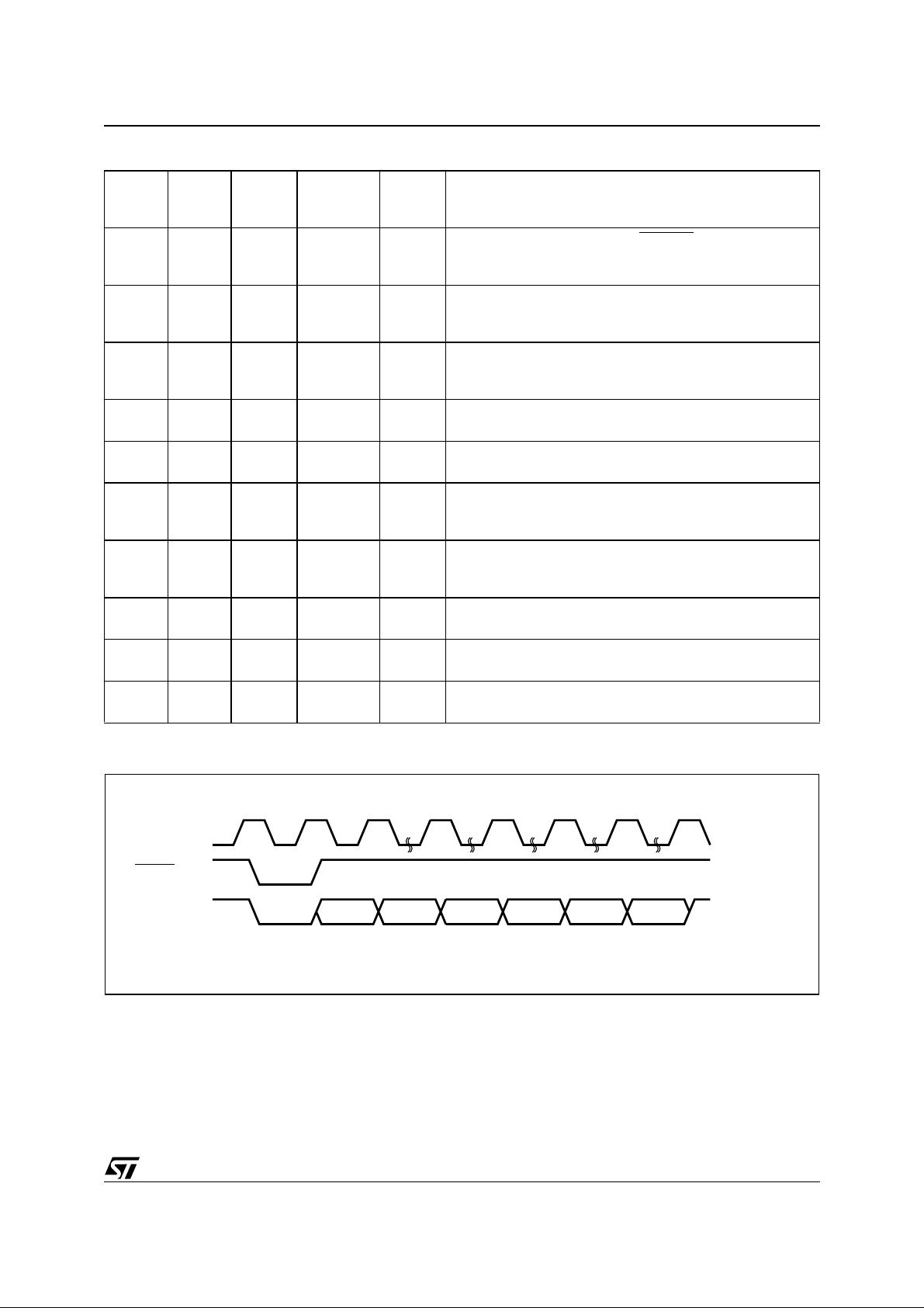
Table 7. LPC Bus Read Field Definitions
Clock
Cycle
Number
Clock
Cycle
Count
Field
LAD0-
LAD3
Memory
I/O
M50LPW041
Description
1 1 START 0000b I
CYCTY
21
PE +
0100b I
DIR
3-10 8 ADDR XXXX I
11 1 TAR 1111b I
12 1 TAR
1111b
(float)
13-14 2 WSYNC 0101b O
15 1 RSYNC 0000b O
16-17 2 DATA XXXX O
18 1 TAR 1111b O
On the rising edge of CLK with LFRAME
Low, the contents
of LAD0-LAD3 must be 0000b to indicate the start of a LPC
cycle.
Indicates the type of cycle. Bits 3:2 must be 01b. Bit 1
indicates the direction of transfer: 0b for read. Bit 0 is ‘0’.
A 32-bit address phase is transferred starting with the most
significant nibble first. See Tables 3, 2 and 6 for the field
description.
The host drives LAD0-LAD3 to 1111b to indicate a
turnaround cycle.
The LPC Flash Memory takes control of LAD0-LAD3 during
O
this cycle.
The LPC Flash Memory drives LAD0-LAD3 to 0101b (short
wait-sync) for two clock cycles, indicating that the data is not
yet available. Two wait-states are always included.
The LPC Flash Memory drives LAD0-LAD3 to 0000b,
indicating that data will be available during the next clock
cycle.
Data transfer is two CLK cycles, starting with the least
significant nibble.
The LPC Flash Memory drives LAD0-LAD3 to 1111b to
indicate a turnaround cycle.
19 1 TAR
1111b
(float)
Figure 5. LPC Bus Read Waveforms
CLK
LFRAME
LAD0-LAD3
Number of
clock cycles
START
CYCTYPE
+ DIR
1182322
N/A
ADDR TAR SYNC DATA TAR
The LPC Flash Memory floats its outputs, the host takes
control of LAD0-LAD3.
AI04429
9/37
Page 10
M50LPW041
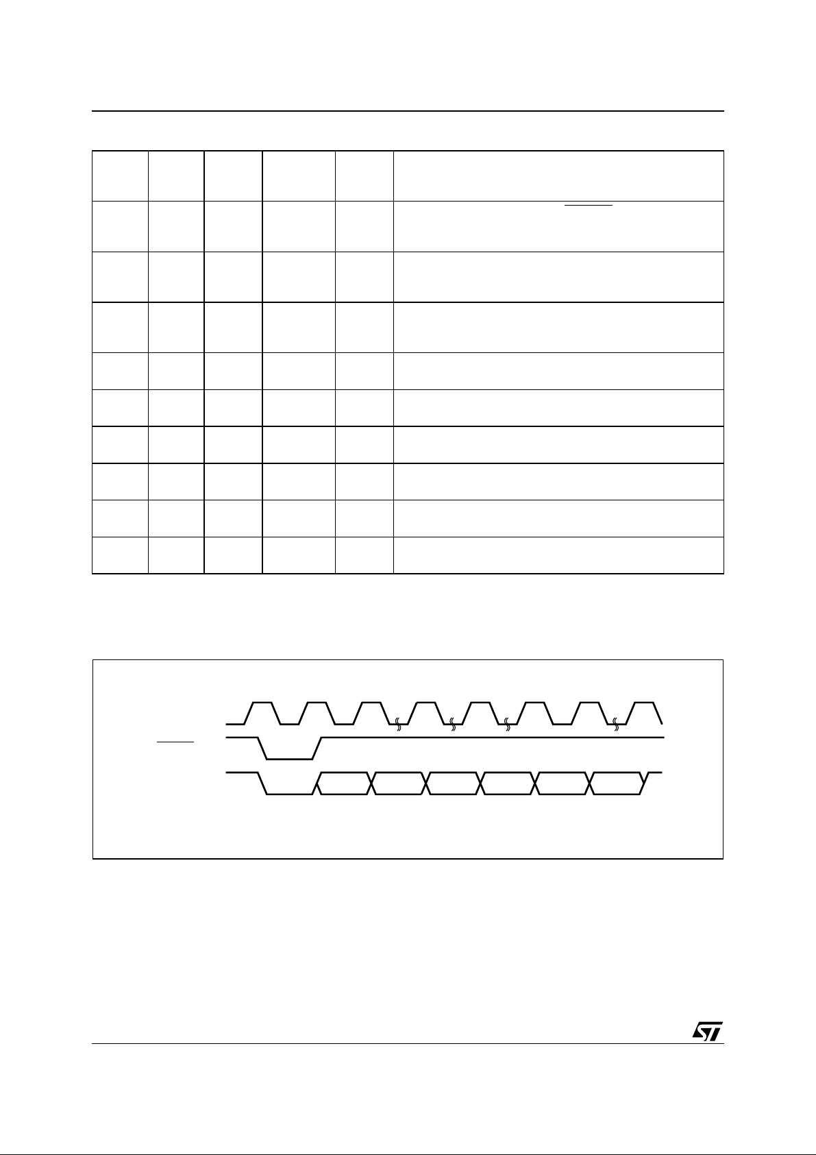
Table 8. LPC Bus Write Field Definitions
Clock
Cycle
Number
Clock
Cycle
Count
Field
LAD0-
LAD3
Memory
I/O
Description
1 1 START 0000b I
CYCTY
21
PE +
011Xb I
DIR
3-10 8 ADDR XXXX I
11-12 2 DATA XXXX I
13 1 TAR 1111b I
14 1 TAR
1111b
(float)
15 1 SYNC 0000b O
16 1 TAR 1111b O
17 1 TAR
1111b
(float)
N/A
On the rising edge of CLK with LFRAME
Low, the contents
of LAD0-LAD3 must be 0000b to indicate the start of a LPC
cycle.
Indicates the type of cycle. Bits 3:2 must be 01b. Bit 1
indicates the direction of transfer: 1b for write. Bit 0 is don’t
care (X).
A 32-bit address phase is transferred starting with the most
significant nibble first. See Tables 3, 2 and 6 for the field
description.
Data transfer is two cycles, starting with the least significant
nibble.
The host drives LAD0-LAD3 to 1111b to indicate a
turnaround cycle.
The LPC Flash Memory takes control of LAD0-LAD3 during
O
this cycle.
The LPC Flash Memory drives LAD0-LAD3 to 0000b,
indicating it has received data or a command.
The LPC Flash Memory drives LAD0-LAD3 to 1111b,
indicating a turnaround cycle.
The LPC Flash Memory floats its outputs and the host takes
control of LAD0-LAD3.
Figure 6. LPC Bus Write Waveforms
CLK
LFRAME
START
1182212
10/37
LAD0-LAD3
Number of
clock cycles
CYCTYPE
+ DIR
ADDR DATA TAR SYNC TAR
AI04430
Page 11
Table 9. A/A Mux Bus Operations
Operation G W RP
Bus Read
Bus Write
Output Disable
Reset
V
IL
V
IH
V
IH
V
or V
IL
IH
V
IH
V
IL
V
IH
VIL or V
Table 10. Manufacturer and Device Codes
Operation G
Manufacturer Code
Device Code
V
IL
V
IL
W RP A18-A1 A0 DQ7-DQ0
V
IH
V
IH
M50LPW041
V
PP
V
IH
V
IH
V
IH
IH
V
IL
V
IH
V
IH
Don’t Care Data Output
Float or VCC or V
Don’t Care Hi-Z
Don’t Care Hi-Z
V
IL
V
IL
PPH
V
V
IL
IH
DQ7-DQ0
Data Input
20h
3Ch
Register for details on the definitions of the Status
Register bits.
If the address falls in a pro tected block then the
Program operation will abort, the data in the
memory array will no t be changed and the S tatus
Register will output the error.
During the Program operation the memory will
only accept the Read Status Register command
and the Program/Erase Suspend command. All
other commands will be ignored. Typical Program
times are given in Table 13.
Note that the Program command cannot change a
bit set at ‘0’ back to ‘1’ and attempting to do so will
not cause any modification on its value. One of the
Erase commands must be used to set all of the
bits in the block to ‘1’.
See Figure 14, Program Flowchart and Pseudo
Code, for a suggested flowchart on using the
Program command.
Quadruple Byte Program Command. The Quadruple Byte Program Comman d c an be only used
in A/A Mux mode to program four adjacent bytes
in the memory array at a time. The four bytes must
differ only for the addresses A0 and A1.
Programming should not be attempted when V
is not at V
is below V
if V
PP
. The operation can also be executed
PPH
, but result could be uncertain.
PPH
PP
Five Bus Write operations are required to issue the
command. The second, the third and the fourth
Bus Write cycle latches respectively the address
and data of the first, the second and the third byte
in the internal state machine. The fifth Bus Write
cycle latches the address and data of the fourth
byte in the internal state machine and starts the
Program/Erase Controller. Once the command is
issued subsequent Bus R ead operations read the
Status Register. See the section on the Status
Register for details on the definitions of the Status
Register bits.
During the Quadruple Byte Program operation the
memory will only accept the Read Status register
command and the Program/Erase Suspe nd command. All other commands will be ignored. Typical
Quadruple Byte Program times are given in Table
13.
Note that the Quadruple Byte Program comm and
cannot change a bit set to ‘0’ back to ‘1’ and
attempting to do so will not cause any modification
on its value. One of the Erase commands must be
used to set all of the bits in the block to ‘1’.
See Figure 15, Quadruple Byte Program Flowchart and Pseudo Code, for a suggested flowchart
on using the Quadruple Byte Program command.
Chip Erase Command. The Chip Erase Command can be only used in A/A Mux mode to erase
the entire chip at a time. Erasing should not be attempted when V
can also be executed if V
is not at V
PP
PPH
is b elow V
PP
. The operation
, but re-
PPH
sult could be uncertain. Two Bus Write operations
are required to issue the com mand and start the
Program/Erase Controller. Once the command is
issued subsequent Bus R ead operations read the
Status Register. See the section on the Status
Register for details on the definitions of the Status
Register bits. During the Chip Erase operation the
memory will only accept the Read Status Register
command. All other commands will be ignored.
Typical Chip Erase times are given in T able 13.
The Chip Erase command sets all of the bits in the
memory to ‘1’. See Figure 17, Chip Erase Flowchart and Pseudo Code, for a suggested flowchart
on using the Chip Erase command.
11/37
Page 12

M50LPW041
Block Erase Command. The Block Erase com-
mand can be used to erase a block. Two Bus Write
operations are required to issue the command; the
second Bus Write cycle latches the block address
in the internal stat e machine and starts th e Program/Erase Controller. Once the command is issued subsequent Bus Read ope rations read the
Status Register. See the section on the Status
Register for details on the definitions of the Status
Register bits.
If the block is protected then the Block Erase
operation will abort, the data in the block will not be
changed and the Status Register will output the
error.
During the Block Erase operation the me mory wi ll
only accept the Read Status Register command
and the Program/Erase Suspend command. All
other commands will be ignored. Typical Block
Erase times are given in Table 13.
The Block Erase command sets all of the bits in
the block to ‘1’. All previous data in the block is
lost.
See Figure 18, Block Erase Flowchart and Pseudo
Code, for a suggested flowchart on using the
Block Erase command.
Clear Status Register Command. The Clear St atus Register command can be used to reset bits 1,
3, 4 and 5 in the Status Register to ‘0’. One Bus
Write is required to issue the Clear Status Register
command. Once the command is issued the memory returns to its previous mode, subs equent Bus
Read operations continue to output the same data.
The bits in the Status Register are stic ky and do
not automatically return to ‘0’ when a new Program
or Erase command is issued. If an error occurs
then it is essential to clear any error bits in the Status Register by issuing the Clear Status Register
command before attempting a new Program or
Erase command.
Program/Erase Suspend Command. The Program/Erase Suspend command can be used to
pause a Program or B lock Erase operation. O ne
Bus Write cycle is required to issue the Program/
Erase Suspend command and pause the Program/Erase Controller. Once the command is issued it is necessary to poll the Program/Erase
Controller Status bit to find out when the Program/
Erase Controller has paused; no other commands
will be accept ed until the Pro gram/ Erase Cont roller has paused. After the Program/Erase Cont roller has paused, the memory will continue to output
the Status Register until another command is issued.
During the polling period between issuing the
Program/Erase Suspend command and the
Program/Erase Controller pausing it is possible for
the operation to complete. Once Program/Erase
Table 11. Read Electronic Signature
Code Address Data
Manufacturer Code 00000h 20h
Device Code 00001h 3Ch
Note: For A19 v al ue, see Tabl e 2.
Controller Status bit indicates that the Program/
Erase Controller is no longer active, the Program
Suspend Status bit or the Erase Suspend Status
bit can be used to d etermine if the opera tion has
completed or is suspended. For timing on the
delay between issuing the Program/Erase
Suspend command and the Program/Erase
Controller pausing see Table 13.
During Program/Erase Suspend the Read
Memory Array, Read Status Register, Read
Electronic Signature and Program/Erase Resume
commands will be accepted by the Command
Interface. Additionally, if the suspe nded operation
was Block Erase then the Program com mand will
also be accepte d; only the blocks no t being erased
may be read or programmed correctly.
See Figures 16, Program Suspend & Resume
Flowchart and Pseudo Code, and 19, Erase
Suspend & Resume Flowchart and Pseudo Code,
for suggested flowcharts on using the Program/
Erase Suspend command.
Program / Erase Resum e Command. The Program/Erase Resume com m and c an be used to restart the Program/Erase Controller after a
Program/Erase Suspend has p aused it. One Bus
Write cycle is required to issue the Program/Erase
Resume command. O nc e the command is iss ued
subsequent Bus Read operations read the Status
Register.
STATUS REGISTER
The Status Register provides information on the
current or previous Program or Erase operation.
Different bits in the Status Register convey
different information and errors on the operation.
To read the Status Register the Read Status
Register command can be issued. The Status
Register is automatically read after Program,
Erase and Program/Erase Resume commands
are issued. The Status Register c an be read from
any address.
The Status Register bits are summarized in Table
14, Status Register Bits. Refer to Table 14 in conjunction with the text descriptions below.
Program/Erase Controller Status (Bit 7). The Progra m/Erase Controller Status bit indicates whether
the Program/Erase Controller is active or inactive.
When the Program/Erase Controller Status bit is
12/37
Page 13

M50LPW041
Table 12. Commands
Bus Write Operations
Command
Cycles
Read Memory Array 1 X FFh
Read Status Register 1 X 70h
Read Electronic Signature
1X 90h
1X 98h
2X 40hPAPD
Program
2X 10hPAPD
Quadruple Byte Program 5 X 30h
Chip Erase 2 X 80h
Block Erase 2 X 20h BA D0h
Clear Status Register 1 X 50h
Program/Erase Suspend 1 X B0h
Program/Erase Resume 1 X D0h
1X 00h
1X 01h
Invalid/Reserved
1X 60h
1X2Fh
1XC0h
Note: X Don’t Care, PA Program Address, PD Program Data, A
Read Memory Array. After a Read M em ory Array command, read the memory as normal unti l another comm and is issued.
Read Status Register. After a Read Status Register command, read the Status Register as normal until another command is issued.
Read Electronic Signature. Af t er a Read Electronic Signature command, read Manufacturer Code, Device Code until another co m -
mand is issued.
Block Erase, Program. After th ese com man ds re ad t he S tat us Re gist er un t il th e comm an d comp l etes and an othe r c omma nd is is sued.
Quadruple Byte Program. This command is only valid in A/A Mux mode. Addresses A
differing only for address bit A0 and A1. After this command read the Status Register until the command completes and another command is issued.
Chip Er ase. This command is only valid in A /A Mux mode. After this command read the St atus Registe r until t he c ommand complete s
and another command is issued.
Clear Status Register. After the Clear St atus Register command bits 1, 3, 4 and 5 in the Stat us Register a re reset to ‘0’.
Program/Erase Susp end. After the Program /Erase Sus pend command has been accept ed, issue Read Mem ory Array, Read Status
Register, Program (during Era se suspend ) and Program/ Erase resum e commands.
Program/Erase Resu me. After the Program/Erase Resume command the suspended Program/Erase operation resumes, read the
Status Register unti l the Program/ E rase Contr ol l er completes and the mem ory returns to Read Mode.
Invalid/Reserved . Do not use In valid or Res erved commands.
1st 2nd 3rd 4th 5th
Addr Data Addr Data Addr Data Addr Data Addr Data
A
PD
1
X
10h
Consecut i ve Addresses, BA Any address in the Block.
1,2,3,4
A
PD
2
, A2, A3 and A4 must be consecutive addresses
1
A
PD
3
A
PD
4
13/37
Page 14

M50LPW041
Table 13. Program and Erase Times
= 0 to 70°C; VCC = 3.0 to 3.6V)
(T
A
Parameter Interface Test Condition Min
Byte Program 10 200
V
Quadruple Byte Program A/A Mux
Chip Erase A/A Mux
Block Program
Block Erase
Program/Erase Suspend to Program pause
Program/Erase Suspend to Block Erase pause
Note: 1. TA = 25°C, VCC = 3.3V
2. This time is obt ai ned executi ng the Quadruple Byte Prog ram Comma nd.
3. Sampled only, not 100% tested.
(3)
A/A Mux
(3)
= 12V ± 5%
PP
V
= 12V ± 5%
PP
V
= 12V ± 5%
PP
< 12V – 5%
V
PP
= 12V ± 5%
V
PP
V
< 12V – 5%
PP
(1)
Typ
10 200
0.1
0.4 5 sec
0.75 8 sec
Max Unit
5sec
(2)
110sec
30
s
µ
s
µ
sec
5
5
s
µ
s
µ
‘0’, the Program/Erase Controller is active; when
the bit is ‘1’, the Program/Erase Controller is inactive.
The Program/Erase Controller Status is ‘0’ immediately after a Program/Erase Su spend c om m and
is issued until the Program/Erase Controller pauses. After the Program/Erase Controller pauses the
bit is ‘1’.
During Program and Erase operation the Program/Erase Controller Status bit can be pol led to
find the end of the operation. The other bits in the
Status Register should not be tested until the Program/Erase Controller completes the operation
and the bit is ‘1’.
After the Program/Erase Cont roller completes its
operation the Erase S tatus, Program Status and
Block Protection Status bits should be tested for
errors.
Erase Suspend Status (Bit 6). The Erase Suspend Status bit indicates that a Block E rase operation has been suspended and is waiting to be
resumed. The Erase Suspend Status should only
be considered valid when the Program/Erase
Controller Status bit is ‘1’ (Program/Erase Controller inactive); after a Program/Erase Suspend command is issued the memory may still complete the
operation rather than entering the Suspend mode.
When the Erase Suspend Status bit is ‘0’ the Program/Erase Controller is active or has com pleted
its operation; when the bit is ‘1’ a Program/Erase
Suspend command has been issued and the
memory is waiting for a Program/Erase Resume
command.
When a Program/Erase Re sume command is issued the Erase Suspend Status bit returns to ‘0’.
Erase Status (Bit 5). The Erase Status bit can be
used to identify if the memory has applied the
maximum number of erase pulses to the block(s)
and still failed to verify that the block(s) has erased
correctly. The Erase Status bit should be read
once the Program/Erase Controller Status bit is ‘1’
(Program/Erase Controller inactive).
When the Erase Status bit is ‘0’ the memory has
successfully verified that the block(s) has erased
correctly; when the Erase Status bit is ‘ 1’ the P rogram/Erase Controller has applied the maximum
number of pulses to the block(s) an d still failed to
verify that the block(s) has erased correctly.
Once the Erase Status bit is set to ‘1’ it can only be
reset to ‘0’ by a Clear Status Register command or
a hardware reset. If it is set to ‘1’ it should be reset
before a new Program or Erase command is issued, otherwise the new command will appear to
fail.
Program Status (Bit 4). The Program Status bit
can be used to identify if the memory has applied
the maximum number of program pulses to the
byte and still failed to verify that the byte has programmed correctly. The Program Status bit should
be read once the Program/Erase Controller Status
bit is ‘1’ (Program/Erase Controller inactive).
When the Program Status bit is ‘0’ the memory has
successfully verified that the byte has programmed correctly; when the Program Status bit is
‘1’ the Program/Erase Controller has applied the
maximum number of pulses to the byte an d still
failed to verify that the byte has program med c orrectly.
14/37
Page 15

M50LPW041
Table 14. Status Register Bits
Operation Bit 7 Bit 6 Bit 5 Bit 4 Bit 2 Bit 1
(1)
Program active 0
Program suspended 1
Program completed successfully 1
Program failure due to Block Protection (LPC Interface only) 1
Program failure due to cell failure 1
Erase active 000000
Block Erase suspended 1 1 0000
Erase completed successfully 1 0 0000
Block Erase failure due to Block Protection (LPC Interface only) 1 0 0001
Erase failure due to failed cell(s) 1 0 1000
Note: 1. F or Program o perations during Erase Suspend Bit 6 is ‘1’, otherwise Bi t 6 is ‘0’.
X
X
X
X
X
0000
(1)
0010
(1)
0000
(1)
0001
(1)
0100
Once the Program Status bit is set to ‘1’ it can only
be reset to ‘0’ by a Clear Status Register command or a hardware reset. If it is set to ‘1’ it should
be reset before a new Program or Erase command
is issued, otherwise the new command will appear
to fail.
Reserved (Bit 3). This status bit is reserved for
future use. Its value should be masked out whenever the status register is read.
Program Suspend Status (Bit 2). The Program
Suspend Status bit indicates that a Program operation has been suspended and is waiting to be resumed. The Program Suspend Status should only
be considered valid when the Program/Erase
Controller Status bit is ‘1’ (Program/Erase Controller inactive); after a Program/Erase Suspend command is issued the memory may still complete the
operation rather than entering the Suspend mode.
When the Program Suspend Status bit is ‘0’ the
Program/Erase Controller is active or has completed its operation; when the bit is ‘1’ a Program/
Erase Suspend command has been issued and
the memory is waiting for a Program/Erase Resume command.
When a Program/Erase Re sume command is issued the Program Suspend Status bit returns to
‘0’.
Block Protection Status (Bit 1). The Block Protection Status bit can be used to identify if the Program or Block Erase operation has tried to modify
the contents of a protected block. When the Block
Protection Status bit is to ‘0’ no Program or Block
Erase operations have been attempted to protected blocks since the last Clear Status Register
command or hardware reset; when the Block Pro-
tection Status bit is ‘ 1’ a Program or B lock Erase
operation has been attempted on a protected
block.
Once it is set to ‘1’ t he Block Protection Status bit
can only be reset to ‘0’ by a Clear Status Register
command or a ha rdware reset. If it is set to ‘1’ it
should be reset before a ne w Program or Block
Erase command is issued, otherwise the new
command will appear to fail.
Using the A/A Mux Interface the Block Protection
Status bit is always ‘0’.
Reserved (Bit 0). Bit 0 of the Status Register is
reserved. Its value should be masked.
LOW PIN COUNT (LPC) INTERFACE
CONFIGURATION REGISTERS
When the Low Pin Count Interface is selected several additional registe rs can be accessed. These
registers control the protection status of the Blocks
and read the General Purpose Input pins. See Table 15 for an example of the Register Configuration map, valid f or the boot mem ory, that is, ID0ID3 can be left floating or driven Low, V
.
IL
Lock Registers
The Lock Registers control the protection status of
the Blocks. Ea ch Bl o ck h as i ts own Lock Register.
Three bits within each Lock Register control the
protection of each block, the Write Lock Bit, the
Read Lock Bit and the Lock Down Bit.
The Lock Registers can be read and written,
though care should be taken when writing as, once
the Lock D own Bit is set , ‘1’ , fu rther m odifications
to the Lock Register cannot be made until cleared,
to ‘0’, by a reset or power-up.
15/37
Page 16

M50LPW041
See Table 16 for details on the bit definitions of the
Lock Registers.
Write Lock. The Write Lock Bit determines
whether the contents of the Block can be modified
(using the Program or Block Erase Command).
When the Write Lock Bit is set, ‘1’, the block is
write protected; any operations that attempt to
change the data in the block will fail and the Status
Register will report the error. When the Write Lock
Bit is reset, ‘0’, the block is not write protected
through the Lock Register and may be modified
unless write protected through some other means.
If Top Bloc k Lock, TB L
Block (Block 7) is write protected and cannot be
modified. Similarly, if Write Protect, WP
V
, then the Ma in Blocks (Blocks 0 to 6) are write
IL
protected and cannot be modified.
After power-up or reset the Write Lock Bit is al-
ways set to ‘1’ (write protected).
Read Lock. The Read Lock bit determines
whether the contents of the Block can be read
(from Read mode). When the Read Lock Bit is set,
‘1’, the block is read prot ected; an y operat ion that
attempts to read the contents of the block will read
00h instead. When the Read Lock Bit is reset, ‘0’,
read operations in the Block return the data programmed into the block as expected.
After power-up or reset the Read Lock B it is always reset to ‘0’ (not read protected).
Lock Down. The Lock Down Bit provides a
mechanism for protecting software data from simple hacking and malicious attack. When the Lock
Down Bit is set, ‘1’, further modification to the
Write Lock, Read Lock and Lock Down Bits cannot
be performed. A reset or power-up is required before changes to these bits can be made. When the
Lock Down Bit is reset, ‘0’, the Write L ock, Read
Lock and Lock Down Bits can be changed.
General Purpose Input Register
The General Purpose Input Register holds the
state of the General Purpose Input pins, GPI0GPI4. When this register is read, the state of these
pins is returned. This register is read-only and writing to it has no effect.
The signals on the General Purpose Input pins
should remain constant throughout the whole Bus
Read cycle in order to guarantee that the correct
data is read.
, is Low, VIL, then the T op
, is Low,
16/37
Page 17

M50LPW041
Table 15. Low Pin Count Register Configuration Map
Mnemonic Register Name
T_BLOCK_LK Top Block Lock Register (Block 7) FF7F0002h 008F0002h 01h R/W
T_MINUS01_LK Top Block [-1] Lock Register (Block 6) FF7E0002h 008E0002h 01h R/W
T_MINUS02_LK Top Block [-2] Lock Register (Block 5) FF7D0002h 008D0002h 01h R/W
T_MINUS03_LK Top Block [-3] Lock Register (Block 4) FF7C0002h 008C0002h 01h R/W
T_MINUS04_LK Top Block [-4] Lock Register (Block 3) FF7B0002h 008B0002h 01h R/W
T_MINUS05_LK Top Block [-5] Lock Register (Block 2) FF7A0002h 008A0002h 01h R/W
T_MINUS06_LK Top Block [-6] Lock Register (Block 1) FF790002h 00890002h 01h R/W
T_MINUS07_LK Top Block [-7] Lock Register (Block 0) FF780002h 00880002h 01h R/W
GPI_REG General Purpose Input Register FF7C0100h 008C0100h N/A R
Note: 1. Thi s map is referred to the boo t memory (I D0-ID3 fl oating or dri ven, Low).
(1)
Memory Address
Top Bottom
Default
Value
Access
17/37
Page 18

M50LPW041
Tabl e 16. Lock R egister Bit Defini t i ons
(1)
Bit Bit Name Value Function
7-3 Reserved
‘1’ Bus Read operations in this Block always return 00h.
2 Read-Lock
Bus read operations in this Block return the Memory Array contents. (Default
‘0’
value).
Changes to the Read-Lock bit and the Write-Lock bit cannot be performed. Once a
‘1’
‘1’ is written to the Lock-Down bit it cannot be cleared to ‘0’; the bit is always reset
1 Lock-Down
to ‘0’ following a Reset (using RP
Read-Lock and Write-Lock can be changed by writing new values to them. (Default
‘0’
value).
Program and Block Erase operations in this Block will set an error in the Status
‘1’
Register. The memory contents will not be changed. (Default value).
or INIT) or after power-up.
0 Write-Lock
Program and Block Erase operations in this Block are executed and will modify the
‘0’
Block contents.
Note: 1. Applies to Top Block Lock Register (T_BLOCK_LK) and Top Block [-1] Lock Register (T_MINUS01_LK) to Top Block [-7] Lock Reg-
Table 17. General Purpose Input Regi s te r D ef i ni tion
ister (T_MINUS07_LK).
(1)
Bit Bit Name Value Function
7-5 Reserved
Input Pin GPI4 is at V
‘1’
4 GPI4
Input Pin GPI4 is at V
‘0’
Input Pin GPI3 is at V
‘1’
3 GPI3
Input Pin GPI3 is at V
‘0’
Input Pin GPI2 is at V
‘1’
2 GPI2
Input Pin GPI2 is at V
‘0’
Input Pin GPI1 is at V
‘1’
1 GPI1
Input Pin GPI1 is at V
‘0’
Input Pin GPI0 is at V
‘1’
0 GPI0
Input Pin GPI0 is at V
‘0’
Note: 1. App l i e s to t h e General Purpose Input Regis t er (GPI_REG).
IH
IL
IH
IL
IH
IL
IH
IL
IH
IL
18/37
Page 19

M50LPW041
Table 18. LPC Interface AC Measurement Conditions
Parameter Value Un it
V
Supply Voltage
CC
Load Capacitance (C
)
L
Input Rise and Fall Times
3.0 to 3.6 V
10 pF
1.4 ns
≤
Input Pulse Voltages
Input and Output Timing Ref. Voltages
Figure 7. LPC Interface AC Testing Input Output Waveforms
0.6 V
CC
0.2 V
CC
Input and Output AC Testing Waveform
IO < I
LO
Output AC Tri-state Testing Waveform
IO > I
LO
IO < I
0.4 V
LO
AI03404
0.2 V
CC
and 0.6 V
CC
0.4 V
CC
CC
V
V
19/37
Page 20

M50LPW041
Table 19. A/A Mux Interface AC Measurement Conditions
Parameter Value Unit
V
Supply Voltage
CC
3.0 to 3.6 V
Load Capacitance (C
Input Rise and Fall Times
)
L
30 pF
10 ns
≤
Input Pulse Voltages 0 to 3 V
Input and Output Timing Ref. Voltages 1.5 V
Figure 8. A/A Mux I nte rfac e AC Testing In put Output Wav ef orm
3V
1.5V
0V
AI01417
Table 20. Impedance
(T
= 25 °C, f = 1 MHz)
A
Symbol Parameter Test Condition Min Max Unit
(1)
C
IN
(1)
C
CLK
(2)
L
PIN
Note: 1. Sampled only, not 100% tested.
2. See PCI Specification.
Input Capacitance
Clock Capacitance
Recommended Pin
Inductance
V
= 0V
IN
V
= 0V
IN
312pF
13 pF
20 nH
20/37
Page 21

M50LPW041
Table 21. DC Characteristics
(T
= 0 to 70°C; VCC = 3.0 to 3.6V)
A
Symbol Parameter Interface Test Condition Min Max Unit
V
V
V
V
V
(INIT)
IH
(INIT)
IL
I
LI
I
R
V
V
I
V
LKO
I
CC1
IH
IL
(2)
LI2
IL
OH
OL
LO
PPH
Input High Voltage
Input Low Voltage
Input High Voltage LPC 1.35
INIT
Input Low Voltage LPC –0.5
INIT
Input Leakage Current
IC, IDx Input Leakage
Current
IC, IDx Input Pull Low
Resistor
Output High Voltage
Output Low Voltage
Output Leakage Curren t
VPP Voltage (Fast
Program/Fast Erase)
(1)
VCC Lockout Volt age
Supply Current (Standby) LPC
LPC
A/A Mux
0.5 V
0.7 V
LPC –0.5
CCVCC
CCVCC
+ 0.5
+ 0.3
0.3 V
CC
A/A Mux -0.5 0.8 V
V
+ 0.5
CC
0.2 V
CC
0V ≤ V
IC, ID0, ID1, ID2, ID3 = V
IN
≤ V
CC
CC
±10
µA
200 µA
20 100 k
LPC I
A/A Mux I
LPC
A/A Mux
0V ≤ V
= –500µA
OH
= –100µA
OH
I
= 1.5mA 0.1 V
OL
I
= 1.8mA
OL
≤ V
OUT
CC
0.9 V
V
CC
CC
– 0.4
CC
0.45 V
±10
µA
11.4 12.6 V
1.8 2.3 V
LFRAME
All other inputs 0.9 VCC to 0.1 V
= 0.9 V
CC
CC
100
µ
VCC = 3.6V, f(CLK) = 33MHz
V
V
V
V
V
Ω
V
V
V
A
I
CC2
Supply Current (Standby) LPC
LFRAME
All other inputs 0.9 VCC to 0.1 V
= 0.1 V
CC
VCC = 3.6V, f(CLK) = 33MHz
= VCC max
Supply Current
I
CC3
I
CC4
I
CC5
I
PP
I
PP1
Note: 1. Sampled only, not 100% tested.
(Any internal operation
active)
Supply Current (Read) A/A Mux
Supply Current
(1)
(Program/Erase)
VPP Supply Current
(Read/Standby)
VPP Supply Current
(1)
(Program/Erase active)
2. Input leakag e currents include Hig h-Z output leakage for all bi -directi onal buffers wi th tri-state output s.
LPC
A/A Mux Program/Erase Controller Active 20 mA
V
CC
f(CLK) = 33MHz
= 0mA
I
OUT
G
= VIH, f = 6MHz
V
V
>
PP
CC
V
= V
PP
CC
V
= 12V ± 5%
PP
CC
10 mA
60 mA
20 mA
400
5
15 mA
21/37
A
µ
A
µ
Page 22

M50LPW041
Table 22. LPC Interface Clock Characteristics
(T
= 0 to 70°C; VCC = 3.0 to 3.6V)
A
Symbol Parameter Test Condition Value Unit
t
CYC
CLK Cycle Time
(1)
Min 30 ns
t
HIGH
t
LOW
CLK High Time Min 11 ns
CLK Low Time Min 11 ns
Min 1 V/ns
CLK Slew Rate peak to peak
Max 4 V/ns
Note: 1. Devi ces on the PC I Bus must work with a ny clock frequency be tween DC an d 33MHz. Be l ow 16MHz dev i ces may be guarantee d
by design rather than tested. Refer to PCI Specification.
Figure 9. LPC Interface Clock Waveform
tCYC
tHIGH tLOW
0.6 V
CC
0.5 V
0.4 V
0.3 V
0.2 V
CC
CC
CC
CC
0.4 VCC,
(minimum)
p-to-p
AI03403
22/37
Page 23

Table 23. LPC Interface AC Signal Timing Characteristics
(T
= 0 to 70 °C; VCC = 3.0 to 3.6V)
A
Symbol
PCI
Symbol
Parameter Test Condition Value Unit
M50LPW041
t
CHQV
(1)
t
CHQX
t
CHQZ
t
AVCH
t
DVCH
t
CHAX
t
CHDX
Note: 1. The timing measurements for Active/Float transitions are defined when the current through the pin equals the leakage current spec-
ification.
2. Applies to all inputs except CLK.
t
t
t
CLK to Data Out
val
CLK to Active
on
(Float to Active Delay)
CLK to Inactive
off
(Active to Float Delay)
t
su
Input Set-up Time
t
h
Input Hold Time
(2)
(2)
Min 2 ns
Max 11 ns
Min 2 ns
Max 28 ns
Min 7 ns
Min 0 ns
Figure 10. LPC Interface AC Signal Timing Waveforms
CLK
LAD0-LAD3
tCHQV
VALID OUTPUT DATA FLOAT OUTPUT DATA VALID INPUT DATA
tCHQZ
tCHQX
tDVCH
tCHDX
VALID
AI04431
23/37
Page 24

M50LPW041
Table 24. Reset AC Characteristics
(T
= 0 to 70°C; VCC = 3.0 to 3.6V)
A
Symbol Parameter Test Condition Value Unit
t
PLPH
t
PLRH
t
PHFL
t
PHWL
t
PHGL
Note: 1. See Chapter 4 of the PCI Specif i cation.
RP or INIT Reset Pulse Width Min 100 ns
RP or INIT Low to Reset
or INIT Slew Rate
RP
(1)
RP or INIT High to LFRAME Low LPC Interface only Min 30
RP High to Write Enable or Output
Enable Low
Figure 11. Reset AC Waveforms
RP, INIT
W, G, LFRAME
Program/Erase Inactive Max 100 ns
Program/Erase Active Max 30
Rising edge only Min 50 mV/ns
A/A Mux Interface only Min 50
tPLPH
tPHWL, tPHGL, tPHFL
tPLRH
s
µ
s
µ
s
µ
RB
AI04432
24/37
Page 25

M50LPW041
Table 25. A/A Mux Interface Read AC Characteristics
(T
= 0 to 70°C; VCC = 3.0 to 3.6V)
A
Symbol Parameter Test Condition Value Unit
t
AVAV
t
AVCL
t
CLAX
t
AVCH
t
CHAX
t
CHQV
t
GLQV
t
PHAV
t
GLQX
t
GHQZ
t
GHQX
Note: 1. G may be delayed up to t
Read Cycle Time Min 250 ns
Row Address Valid to RC Low Min 50 ns
RC Low to Row Address Transition Min 50 ns
Column Address Valid to RC high Min 50 ns
RC High to Column Address Transition Min 50 ns
(1)
RC High to Output Valid Max 150 ns
(1)
Output Enable Low to Output Valid Max 50 ns
RP High to Row Address Valid Min 1
Output Enable Low to Output Transition Min 0 ns
Output Enable High to Output Hi-Z Max 50 ns
Output Hold from Output Enable High Min 0 ns
– t
CHQV
after the ri si ng edge of RC without impact on t
GLQV
Figure 12. A/A Mux Interface Read AC Waveforms
tAVAV
CHQV
s
µ
.
A0-A10
RC
G
DQ0-DQ7
W
RP
ROW ADDR VALID NEXT ADDR VALID
tAVCL tAVCH
tCLAX tCHAX
tPHAV
COLUMN ADDR VALID
tCHQV
tGLQV
tGLQX
tGHQZ
tGHQX
VALID
AI03406
25/37
Page 26

M50LPW041
Table 26. A/A Mux Interface Write AC Characteristics
(T
= 0 to 70°C; VCC = 3.0 to 3.6V)
A
Symbol Parameter Test Condition Value Unit
t
WLWH
t
DVWH
t
WHDX
t
AVCL
t
CLAX
t
AVCH
t
CHAX
t
WHWL
t
CHWH
t
WHGL
t
WHRL
Write Enable Low to Write Enable High Min 100 ns
Data Valid to Write Enable High Min 50 ns
Write Enable High to Data Transition Min 5 ns
Row Address Valid to RC Low Min 50 ns
RC Low to Row Address Transition Min 50 ns
Column Address Valid to RC High Min 50 ns
RC High to Column Address Transition Min 50 ns
Write Enable High to Write Enable Low Min 100 ns
RC High to Write Enable High Min 50 ns
Write Enable High to Output Enable Low Min 30 ns
Write Enable High to RB Low Min 0 ns
26/37
Page 27

Figure 13. A/A Mux Interface Write AC Waveforms
M50LPW041
A0-A10
RC
W
G
RB
DQ0-DQ7
Write erase or
program setup
R1
tAVCL
tWLWH
C1
tCLAX
tWHWL
Write erase confirm or
valid address and data
R2 C2
tAVCH
tCHAX
D
IN1
tWHRL
Automated erase
or program delay
tCHWH
D
IN2
tWHGL
tWHDXtDVWH
Read Status
Register Data
VALID SRD
Ready to write
another command
AI06817
27/37
Page 28

M50LPW041
Figure 14. Program Flow c hart and Ps e ud o C ode
Start
LPC
Interface
Only
Write 40h or 10h
Write Address
& Data
Read Status
Register
b7 = 1
YES
b4 = 0
YES
b1 = 0
YES
End
NO
NO
NO
NO
Suspend
Program to Protected
Block Error (1, 2)
YES
Suspend
Program
Error (1, 2)
Program command:
– write 40h or 10h
– write Address & Data
(memory enters read status state after
the Program command)
do:
–read Status Register if Program/Erase
Suspend command given execute
suspend program loop
Loop
while b7 = 1
If b4 = 1, Program error:
– error handler
If b1 = 1, Program to protected block error:
– error handler
AI06818
Note: 1. A Status check of b1 (Protected Block) and b4 (Program Error) can be made after each Program operation by following the correct
command sequence.
2. If an error is found, the Stat us Registe r must be clea red before fu rt her Program / Erase Con troller operations.
28/37
Page 29

M50LPW041
Figure 15. Quadruple Byte Program Flowchart and Pseudo Code (A/A Mux Interface Only)
Start
Write 30h
Write Address 1
Write Address 2
Write Address 3
Write Address 4
Read Status
& Data 1
& Data 2
& Data 3
& Data 4
Register
b7 = 1
b4 = 0
(3)
(3)
(3)
(3)
YES
NO
NO
NO
Suspend
YES
Suspend
Program
Error (1, 2)
Loop
Quadruple Byte Program command:
– write 30h
– write Address 1 & Data 1
– write Address 2 & Data 2
– write Address 3 & Data 3
– write Address 4 & Data 4
(memory enters read status state after
the Quadruple Byte Program command)
do:
– read Status Register if Program/Erase
Suspend command given execute
suspend program loop
while b7 = 1
If b4 = 1, Program error:
– error handler
(3)
(3)
(3)
(3)
YES
End
Note: 1. A St atus check of b4 (Program Er ror) can be ma de after eac h Program operation by f ol l owing the correct command sequence.
2. If an error is found, the Stat us Register must be cleared befor e further Program/Erase Contr ol l er operations.
3. Address 1, Address 2, Address 3 and Address 4 must be consecuti ve addresse s differing only for addre ss bits A0 and A 1.
AI06819
29/37
Page 30

M50LPW041
Figure 16. Program Suspend and Resume Flowchart, and Pseudo Code
Start
Write B0h
Program/Erase Suspend command:
Write 70h
Read Status
Register
– write B0h
– write 70h
do:
– read Status Register
b7 = 1
YES
b2 = 1
YES
Write a read
Command
Read data from
another address
Write D0h
Program Continues
NO
NO
Program Complete
Write FFh
Read Data
while b7 = 1
If b2 = 0 Program completed
Program/Erase Resume command:
– write D0h to resume the program
– if the Program operation completed
then this is not necessary.
The device returns to Read as
normal (as if the Program/Erase
suspend was not issued).
AI03408
30/37
Page 31

Figure 17. Chip Erase Flowchart and Pseudo Code (A/A Mux Interface Only)
Start
M50LPW041
Write 80h
Write 10h
Read Status
Register
YES
YES
YES
NO
NO
NO
Command
Sequence Error (1)
b7 = 1
b4, b5 = 0
b5 = 0 Erase Error (1)
End
Chip Erase command:
– write 80h
– write 10h
(memory enters read Status Register after
the Chip Erase command)
do:
– read Status Register
while b7 = 1
If b4, b5 = 1, Command sequence error:
– error handler
If b5 = 1, Erase error:
– error handler
AI06820
Note: 1. If an error is found, the Status Register must be cleared befor e further Program/Erase Contr ol l er operations.
31/37
Page 32

M50LPW041
Figure 18. Block Erase Flowchart and Pseudo Code
Start
LPC
Interface
Only
Write 20h
Write Block Address
& D0h
Read Status
Register
b7 = 1
b4, b5 = 0
b5 = 0 Erase Error (1)
b1 = 0
End
NO
YES
NO
YES
NO
YES
NO
YES
Suspend
Sequence Error (1)
Erase to Protected
NO
YES
Command
Block Error (1)
Block Erase command:
– write 20h
– write Block Address & D0h
(memory enters read Status Register after
the Block Erase command)
do:
– read Status Register
– if Program/Erase Suspend command
given execute suspend erase loop
Suspend
Loop
while b7 = 1
If b4, b5 = 1, Command sequence error:
– error handler
If b5 = 1, Erase error:
– error handler
If b1 = 1, Erase to protected block error:
– error handler
AI04434
Note: 1. If an error is found, the Status Register must be cleared befor e further Program/Erase Contr ol l er operations.
32/37
Page 33

Figure 19. Erase Suspend and Resume Flow chart, and Pseudo Code
Start
Write B0h
Program/Erase Suspend command:
Write 70h
– write B0h
– write 70h
M50LPW041
Read Status
Register
b7 = 1
YES
b6 = 1
YES
Read data from
another block
or
Program
Write D0h
Erase Continues
NO
NO
Erase Complete
Write FFh
Read Data
do:
– read Status Register
while b7 = 1
If b6 = 0, Erase completed
Program/Erase Resume command:
– write D0h to resume erase
– if the Erase operation completed
then this is not necessary.
The device returns to Read as
normal (as if the Program/Erase
suspend was not issued).
AI03410
33/37
Page 34

M50LPW041
Table 27. Ordering Information Scheme
Example: M50LPW041 K 1 T
Device Type
M50
Architecture
LP = Low Pin Count Interface
Operating Voltage
W = 3.0 to 3.6V
Device Function
041 = 4 Mbit (512Kb x8), Uniform Block
Package
K = PLCC32
N = TSOP40: 10 x 20 mm
Temperature Range
1 = 0 to 70 °C
Option
T = Tape & Reel Packing
For a list of available options or for furt her information on any aspect of this device, please contact the ST
Sales Office nearest to you.
Table 28. Revision History
Date Version Revision Details
07-Jun-2002 -01 First Issue
24-Jul-2002 -02 Temperature Range 5 removed, and document promoted to “Preliminary Data”
16-Sep-2002 2.1
TSOP40 package added. Revision numbering modified: a minor revision will be
indicated by incrementing the digit after the dot, and a major revision, by incrementing
the digit before the dot (revision version 02 equals 2.0).
34/37
Page 35

PLCC32 – 32 lead Plastic Leaded Chip Carrier, Package Outline
M50LPW041
E3
Note: Drawing is not to scale.
D
D1
1 N
D3
D2 D2
E1 E
F
0.51 (.020)
1.14 (.045)
R
A1
A2
B1
E2
e
B
E2
A
CP
PLCC-A
PLCC32 – 32 lead Plastic Leaded Chip Carrier, Package Mechanical Data
Symbol
Typ Min Max Typ Min Max
A 3.18 3.56 0.125 0 .140
A1 1.53 2.41 0.060 0.095
A2 0.38 – 0.015 –
B 0.33 0.53 0.013 0 .021
B1 0.66 0.81 0.026 0.032
CP 0.10 0.004
D 12.32 12.57 0.485 0.495
D1 11.35 11.51 0.447 0.453
D2 4.78 5.66 0.188 0.223
D3 7.62 – – 0.300 – –
E 14.86 15.1 1 0.585 0.595
E1 13.89 14.0 5 0.547 0.553
E2 6.05 6.93 0.238 0 .273
E3 10.16 – – 0.400 – –
e 1.27 – – 0.050 – –
F 0.00 0.13 0. 000 0.005
N32 32
R 0.89 – – 0.035 – –
millimeters inches
35/37
Page 36

M50LPW041
TSOP40 – 40 lead Plastic Thin Small Outline, 10 x 20mm, Package Outline
A2
Note: Drawing is not to scale.
1 N
N/2
DIE
TSOP-a
D1
D
E
A
C
e
B
CP
LA1 α
TSOP40 – 40 lead Plastic Thin Small Outline, 10 x 20mm, Package Mechan ic al Data
Symbol
Typ Min Max Typ Min Max
millimeters inches
A 1.20 0 0.0472
A1 0.050 0.15 0 0.0020 0.0059
A2 0.950 1.05 0 0.0374 0.0413
B 0.170 0.27 0 0.0067 0.0106
C 0.100 0.210 0.0039 0.0083
D 19.800 20.200 0.7795 0.7953
D1 18.300 18.500 0.7205 0.7283
E 9.900 10.100 0.3 898 0.3976
e 0.500 – – 0.0197 – –
L 0.500 0.700 0.0197 0.0276
α
0° 5° 0° 5°
N40 40
CP 0.100 0 .0039
36/37
Page 37

M50LPW041
Information furnished is believed to be ac curate and reli able. Howev er, STMicroel ectronics assumes no responsibilit y for the consequence s
of use of such information nor for any infringement of patents or other rights of third parties which may result from its use. No license is granted
by implic ation or otherwise under any patent or patent rights of STMi croelectr onics. Specifications mentioned in thi s publicati on are subject
to change without notice. This publication supersedes and replaces all information previously supplied. STMicroelectronics products are not
authorized for use as cri tical comp onents in life support dev i ces or systems wi t hout express written ap proval of STMi croelect ro nics.
The ST log o i s registered trademark of STMicroelectronics
All other nam es are the pro perty of their respective owners
© 2002 STMicroelectronics - All Rights Reserved
STMicroelectron ic s group of com panies
Austra lia - Brazil - Can ada - China - Finl and - France - Germany - Hong Kong -
India - Israel - Italy - Japan - Malay sia - Malta - M orocco - Sing apore - Spai n - S weden - Switz erland - Un it ed Kingdom - United States.
www.st.com
37/37
 Loading...