

Page 1

查询M50FW040供应商
FEATURES SUMMARY
■ SUPPLY VOLTAGE
–V
–V
■ TWO INTERFACES
– Firmware Hub (FWH) Interface for
– Address/Address Multiplexed (A/A Mux)
■ FIRMWARE HUB (FWH) HARDWARE
INTERFACE MODE
– 5 Signal Communication Interface
– Hardware Write Protect Pins for Block
– Register Based Read and Write
– 5 Additional General Purpose Inputs for
– Synchronized with 33MHz PCI clock
■ PROGRAMMING TIME: 10µs typical
■ 8 UNIFORM 64 Kbyte MEMORY BLOCKS
■ PROGRAM/ERASE CONTROLLER
– Embedded Byte Program and Block
– Status Register Bits
■ PROGRAM and ERASE SUSPEND
– Read other Blocks during Program/Erase
– Program other Blocks during Erase
■ FOR USE in PC BIOS APPLICAT ION S
■ ELECTRONIC SIGNATURE
– Manufacturer Code: 20h
– Device Code: 2Ch
= 3V to 3.6V for Program, Erase and
CC
Read Operations
= 12V for Fast Erase (optional)
PP
embedded operation with PC Chipsets.
Interface for programming equipment
compatibility.
supporting Read and Write Operations
Protection
Protection
platform design flexibility
Erase algorithms
Suspend
Suspend
M50FW040
4 Mbit (512Kb x8, Uniform Block)
3V Supply Firmware Hub Flash Memory
Figure 1. Packages
PLCC32 (K)
TSOP32 (NB)
8 x 14mm
TSOP40 (N)
10 x 20mm
1/41November 2004
Page 2

M50FW040
TABLE OF CONTENTS
FEATURES SUMMARY . . . . . . . . . . . . . . . . . . . . . . . . . . . . . . . . . . . . . . . . . . . . . . . . . . . . . . . . . . . . . 1
Figure 1. Packages. . . . . . . . . . . . . . . . . . . . . . . . . . . . . . . . . . . . . . . . . . . . . . . . . . . . . . . . . . . . . . 1
SUMMARY DESCRIPTION. . . . . . . . . . . . . . . . . . . . . . . . . . . . . . . . . . . . . . . . . . . . . . . . . . . . . . . . . . . 6
Figure 2. Logic Diagram (FWH Interface). . . . . . . . . . . . . . . . . . . . . . . . . . . . . . . . . . . . . . . . . . . . . 6
Table 1. Signal Names (FWH Interface) . . . . . . . . . . . . . . . . . . . . . . . . . . . . . . . . . . . . . . . . . . . . . 6
Figure 3. Logic Diagram (A/A Mux Interface). . . . . . . . . . . . . . . . . . . . . . . . . . . . . . . . . . . . . . . . . . 7
Table 2. Signal Names (A/A Mux Interface) . . . . . . . . . . . . . . . . . . . . . . . . . . . . . . . . . . . . . . . . . . 7
Figure 4. PLCC Connections . . . . . . . . . . . . . . . . . . . . . . . . . . . . . . . . . . . . . . . . . . . . . . . . . . . . . . 7
Figure 5. TSOP32 Connections . . . . . . . . . . . . . . . . . . . . . . . . . . . . . . . . . . . . . . . . . . . . . . . . . . . . 8
Figure 6. TSOP40 Connections . . . . . . . . . . . . . . . . . . . . . . . . . . . . . . . . . . . . . . . . . . . . . . . . . . . . 8
SIGNAL DESCRIPTIONS . . . . . . . . . . . . . . . . . . . . . . . . . . . . . . . . . . . . . . . . . . . . . . . . . . . . . . . . . . . . 9
Firmware Hub (FWH) Signal Descriptions . . . . . . . . . . . . . . . . . . . . . . . . . . . . . . . . . . . . . . . . . . 9
Input/Output Communications (FWH0-FWH3). . . . . . . . . . . . . . . . . . . . . . . . . . . . . . . . . . . . . . . . . . 9
Input Communication Frame (FWH4).. . . . . . . . . . . . . . . . . . . . . . . . . . . . . . . . . . . . . . . . . . . . . . . .9
Identification Inputs (ID0-ID3).. . . . . . . . . . . . . . . . . . . . . . . . . . . . . . . . . . . . . . . . . . . . . . . . . . . . . . 9
General Purpose Inputs (FGPI0-FGPI4). . . . . . . . . . . . . . . . . . . . . . . . . . . . . . . . . . . . . . . . . . . . . . 9
Interface Configuration (IC). . . . . . . . . . . . . . . . . . . . . . . . . . . . . . . . . . . . . . . . . . . . . . . . . . . . . . . . 9
Interface Reset (RP
CPU Reset (INIT
Clock (CLK). . . . . . . . . . . . . . . . . . . . . . . . . . . . . . . . . . . . . . . . . . . . . . . . . . . . . . . . . . . . . . . . . . . . 9
Top Block Lock (TBL
Write Protect (WP
Reserved for Future Use (RFU). . . . . . . . . . . . . . . . . . . . . . . . . . . . . . . . . . . . . . . . . . . . . . . . . . . . 10
Address/Address Multiplexed (A/A Mux) Signal Descriptions . . . . . . . . . . . . . . . . . . . . . . . . . 10
Address Inputs (A0-A10). . . . . . . . . . . . . . . . . . . . . . . . . . . . . . . . . . . . . . . . . . . . . . . . . . . . . . . . . 10
Data Inputs/Outputs (DQ0-DQ7). . . . . . . . . . . . . . . . . . . . . . . . . . . . . . . . . . . . . . . . . . . . . . . . . . . 10
Output Enable (G
Write Enable (W
Row/Column Address Select (RC
Ready/Busy Output (RB
Supply Signal Descriptions . . . . . . . . . . . . . . . . . . . . . . . . . . . . . . . . . . . . . . . . . . . . . . . . . . . . . 10
V
Supply Voltage. . . . . . . . . . . . . . . . . . . . . . . . . . . . . . . . . . . . . . . . . . . . . . . . . . . . . . . . . . . . . 10
CC
Optional Supply Voltage. . . . . . . . . . . . . . . . . . . . . . . . . . . . . . . . . . . . . . . . . . . . . . . . . . . . . . 10
V
PP
V
Ground. . . . . . . . . . . . . . . . . . . . . . . . . . . . . . . . . . . . . . . . . . . . . . . . . . . . . . . . . . . . . . . . . . . 10
SS
Table 3. Block Addresses . . . . . . . . . . . . . . . . . . . . . . . . . . . . . . . . . . . . . . . . . . . . . . . . . . . . . . . 10
).. . . . . . . . . . . . . . . . . . . . . . . . . . . . . . . . . . . . . . . . . . . . . . . . . . . . . . . . . . . . . 9
). . . . . . . . . . . . . . . . . . . . . . . . . . . . . . . . . . . . . . . . . . . . . . . . . . . . . . . . . . . . . . . . 9
).. . . . . . . . . . . . . . . . . . . . . . . . . . . . . . . . . . . . . . . . . . . . . . . . . . . . . . . . . . . . 9
). . . . . . . . . . . . . . . . . . . . . . . . . . . . . . . . . . . . . . . . . . . . . . . . . . . . . . . . . . . . . . . 9
). . . . . . . . . . . . . . . . . . . . . . . . . . . . . . . . . . . . . . . . . . . . . . . . . . . . . . . . . . . . . . 10
). . . . . . . . . . . . . . . . . . . . . . . . . . . . . . . . . . . . . . . . . . . . . . . . . . . . . . . . . . . . . . . 10
). . . . . . . . . . . . . . . . . . . . . . . . . . . . . . . . . . . . . . . . . . . . . . . . . . 10
). . . . . . . . . . . . . . . . . . . . . . . . . . . . . . . . . . . . . . . . . . . . . . . . . . . . . . . . . 10
BUS OPERATIONS. . . . . . . . . . . . . . . . . . . . . . . . . . . . . . . . . . . . . . . . . . . . . . . . . . . . . . . . . . . . . . . . 11
Firmware Hub (FWH) Bus Operations . . . . . . . . . . . . . . . . . . . . . . . . . . . . . . . . . . . . . . . . . . . . . 11
Bus Read. . . . . . . . . . . . . . . . . . . . . . . . . . . . . . . . . . . . . . . . . . . . . . . . . . . . . . . . . . . . . . . . . . . . . 11
Bus Write. . . . . . . . . . . . . . . . . . . . . . . . . . . . . . . . . . . . . . . . . . . . . . . . . . . . . . . . . . . . . . . . . . . . . 11
Bus Abort. . . . . . . . . . . . . . . . . . . . . . . . . . . . . . . . . . . . . . . . . . . . . . . . . . . . . . . . . . . . . . . . . . . . . 11
2/41
Page 3

M50FW040
Standby. . . . . . . . . . . . . . . . . . . . . . . . . . . . . . . . . . . . . . . . . . . . . . . . . . . . . . . . . . . . . . . . . . . . . . 11
Reset. . . . . . . . . . . . . . . . . . . . . . . . . . . . . . . . . . . . . . . . . . . . . . . . . . . . . . . . . . . . . . . . . . . . . . . . 11
Block Protection. . . . . . . . . . . . . . . . . . . . . . . . . . . . . . . . . . . . . . . . . . . . . . . . . . . . . . . . . . . . . . . . 11
Address/Address Multiplexed (A/A Mux) Bus Operations. . . . . . . . . . . . . . . . . . . . . . . . . . . . . 11
Bus Read. . . . . . . . . . . . . . . . . . . . . . . . . . . . . . . . . . . . . . . . . . . . . . . . . . . . . . . . . . . . . . . . . . . . . 12
Bus Write. . . . . . . . . . . . . . . . . . . . . . . . . . . . . . . . . . . . . . . . . . . . . . . . . . . . . . . . . . . . . . . . . . . . . 12
Output Disable. . . . . . . . . . . . . . . . . . . . . . . . . . . . . . . . . . . . . . . . . . . . . . . . . . . . . . . . . . . . . . . . . 12
Reset. . . . . . . . . . . . . . . . . . . . . . . . . . . . . . . . . . . . . . . . . . . . . . . . . . . . . . . . . . . . . . . . . . . . . . . . 12
Table 4. FWH Bus Read Field Definitions. . . . . . . . . . . . . . . . . . . . . . . . . . . . . . . . . . . . . . . . . . . 12
Figure 7. FWH Bus Read Waveforms. . . . . . . . . . . . . . . . . . . . . . . . . . . . . . . . . . . . . . . . . . . . . . . 13
Table 5. FWH Bus Write Field Definitions . . . . . . . . . . . . . . . . . . . . . . . . . . . . . . . . . . . . . . . . . . . 13
Figure 8. FWH Bus Write Waveforms. . . . . . . . . . . . . . . . . . . . . . . . . . . . . . . . . . . . . . . . . . . . . . . 13
COMMAND INTERFACE . . . . . . . . . . . . . . . . . . . . . . . . . . . . . . . . . . . . . . . . . . . . . . . . . . . . . . . . . . . 14
Read Memory Array Command. . . . . . . . . . . . . . . . . . . . . . . . . . . . . . . . . . . . . . . . . . . . . . . . . . . .14
Read Status Register Command. . . . . . . . . . . . . . . . . . . . . . . . . . . . . . . . . . . . . . . . . . . . . . . . . . .14
Read Electronic Signature Command . . . . . . . . . . . . . . . . . . . . . . . . . . . . . . . . . . . . . . . . . . . . . . . 14
Program Command . . . . . . . . . . . . . . . . . . . . . . . . . . . . . . . . . . . . . . . . . . . . . . . . . . . . . . . . . . . . . 14
Erase Command . . . . . . . . . . . . . . . . . . . . . . . . . . . . . . . . . . . . . . . . . . . . . . . . . . . . . . . . . . . . . . . 14
Clear Status Register Command. . . . . . . . . . . . . . . . . . . . . . . . . . . . . . . . . . . . . . . . . . . . . . . . . . . 14
Program/Erase Suspend Command . . . . . . . . . . . . . . . . . . . . . . . . . . . . . . . . . . . . . . . . . . . . . . . . 15
Program/Erase Resume Command . . . . . . . . . . . . . . . . . . . . . . . . . . . . . . . . . . . . . . . . . . . . . . . . 15
Table 6. Read Electronic Signature. . . . . . . . . . . . . . . . . . . . . . . . . . . . . . . . . . . . . . . . . . . . . . . .15
Table 7. Commands . . . . . . . . . . . . . . . . . . . . . . . . . . . . . . . . . . . . . . . . . . . . . . . . . . . . . . . . . . . 16
STATUS REGISTER . . . . . . . . . . . . . . . . . . . . . . . . . . . . . . . . . . . . . . . . . . . . . . . . . . . . . . . . . . . . . . . 17
Program/Erase Controller Status (Bit 7) . . . . . . . . . . . . . . . . . . . . . . . . . . . . . . . . . . . . . . . . . . . . .17
Erase Suspend Status (Bit 6) . . . . . . . . . . . . . . . . . . . . . . . . . . . . . . . . . . . . . . . . . . . . . . . . . . . . . 17
Erase Status (Bit 5) . . . . . . . . . . . . . . . . . . . . . . . . . . . . . . . . . . . . . . . . . . . . . . . . . . . . . . . . . . . . . 17
Program Status (Bit 4) . . . . . . . . . . . . . . . . . . . . . . . . . . . . . . . . . . . . . . . . . . . . . . . . . . . . . . . . . . . 17
V
Status (Bit 3). . . . . . . . . . . . . . . . . . . . . . . . . . . . . . . . . . . . . . . . . . . . . . . . . . . . . . . . . . . . . . . 17
PP
Program Suspend Status (Bit 2) . . . . . . . . . . . . . . . . . . . . . . . . . . . . . . . . . . . . . . . . . . . . . . . . . . . 18
Block Protection Status (Bit 1). . . . . . . . . . . . . . . . . . . . . . . . . . . . . . . . . . . . . . . . . . . . . . . . . . . . . 18
Reserved (Bit 0). . . . . . . . . . . . . . . . . . . . . . . . . . . . . . . . . . . . . . . . . . . . . . . . . . . . . . . . . . . . . . . . 18
Table 8. Status Register Bits . . . . . . . . . . . . . . . . . . . . . . . . . . . . . . . . . . . . . . . . . . . . . . . . . . . . . 18
FIRMWARE HUB (FWH) INTERFACE CONFIGURATION REGISTERS . . . . . . . . . . . . . . . . . . . . . . 19
Lock Registers. . . . . . . . . . . . . . . . . . . . . . . . . . . . . . . . . . . . . . . . . . . . . . . . . . . . . . . . . . . . . . . . 19
Write Lock . . . . . . . . . . . . . . . . . . . . . . . . . . . . . . . . . . . . . . . . . . . . . . . . . . . . . . . . . . . . . . . . . . . . 19
Read Lock . . . . . . . . . . . . . . . . . . . . . . . . . . . . . . . . . . . . . . . . . . . . . . . . . . . . . . . . . . . . . . . . . . . . 19
Lock Down. . . . . . . . . . . . . . . . . . . . . . . . . . . . . . . . . . . . . . . . . . . . . . . . . . . . . . . . . . . . . . . . . . . . 19
Firmware Hub (FWH) General Purpose Input Register . . . . . . . . . . . . . . . . . . . . . . . . . . . . . . . 19
Manufacturer Code Register . . . . . . . . . . . . . . . . . . . . . . . . . . . . . . . . . . . . . . . . . . . . . . . . . . . . 19
Device Code Register . . . . . . . . . . . . . . . . . . . . . . . . . . . . . . . . . . . . . . . . . . . . . . . . . . . . . . . . . . 19
Firmware Hub (FWH) General Purpose Input Register . . . . . . . . . . . . . . . . . . . . . . . . . . . . . . . 19
Manufacturer Code Register . . . . . . . . . . . . . . . . . . . . . . . . . . . . . . . . . . . . . . . . . . . . . . . . . . . . 19
3/41
Page 4

M50FW040
Device Code Register . . . . . . . . . . . . . . . . . . . . . . . . . . . . . . . . . . . . . . . . . . . . . . . . . . . . . . . . . . 19
Table 9. Firmware Hub Register Configuration Map . . . . . . . . . . . . . . . . . . . . . . . . . . . . . . . . . . . 20
Table 10. Lock Register Bit Definitions . . . . . . . . . . . . . . . . . . . . . . . . . . . . . . . . . . . . . . . . . . . . . . 20
Table 11. General Purpose Inputs Register Definition . . . . . . . . . . . . . . . . . . . . . . . . . . . . . . . . . . 20
PROGRAM AND ERASE TIMES . . . . . . . . . . . . . . . . . . . . . . . . . . . . . . . . . . . . . . . . . . . . . . . . . . . . .21
Table 12. Program and Erase Times. . . . . . . . . . . . . . . . . . . . . . . . . . . . . . . . . . . . . . . . . . . . . . . . 21
MAXIMUM RATING. . . . . . . . . . . . . . . . . . . . . . . . . . . . . . . . . . . . . . . . . . . . . . . . . . . . . . . . . . . . . . . . 22
Table 13. Absolute Maximum Ratings. . . . . . . . . . . . . . . . . . . . . . . . . . . . . . . . . . . . . . . . . . . . . . . 22
DC AND AC PARAMETERS. . . . . . . . . . . . . . . . . . . . . . . . . . . . . . . . . . . . . . . . . . . . . . . . . . . . . . . . . 23
Table 14. Operating Conditions. . . . . . . . . . . . . . . . . . . . . . . . . . . . . . . . . . . . . . . . . . . . . . . . . . . . 23
Table 15. FWH Interface AC Measurement Conditions. . . . . . . . . . . . . . . . . . . . . . . . . . . . . . . . . . 23
Table 16. A/A Mux Interface AC Measurement Conditions . . . . . . . . . . . . . . . . . . . . . . . . . . . . . . . 23
Figure 9. FWH Interface AC Testing Input Output Waveforms. . . . . . . . . . . . . . . . . . . . . . . . . . . . 23
Figure 10.A/A Mux Interface AC Testing Input Output Waveform. . . . . . . . . . . . . . . . . . . . . . . . . . 24
Table 17. Impedance. . . . . . . . . . . . . . . . . . . . . . . . . . . . . . . . . . . . . . . . . . . . . . . . . . . . . . . . . . . . 24
Table 18. DC Characteristics. . . . . . . . . . . . . . . . . . . . . . . . . . . . . . . . . . . . . . . . . . . . . . . . . . . . . . 25
Figure 11.FWH Interface Clock Waveform . . . . . . . . . . . . . . . . . . . . . . . . . . . . . . . . . . . . . . . . . . . 26
Table 19. FWH Interface Clock Characteristics. . . . . . . . . . . . . . . . . . . . . . . . . . . . . . . . . . . . . . . . 26
Figure 12.FWH Interface AC Signal Timing Waveforms . . . . . . . . . . . . . . . . . . . . . . . . . . . . . . . . . 27
Table 20. FWH Interface AC Signal Timing Characteristics . . . . . . . . . . . . . . . . . . . . . . . . . . . . . . 27
Figure 13.Reset AC Waveforms . . . . . . . . . . . . . . . . . . . . . . . . . . . . . . . . . . . . . . . . . . . . . . . . . . . 28
Table 21. Reset AC Characteristics. . . . . . . . . . . . . . . . . . . . . . . . . . . . . . . . . . . . . . . . . . . . . . . . . 28
Figure 14.A/A Mux Interface Read AC Waveforms . . . . . . . . . . . . . . . . . . . . . . . . . . . . . . . . . . . . . 29
Table 22. A/A Mux Interface Read AC Characteristics . . . . . . . . . . . . . . . . . . . . . . . . . . . . . . . . . . 29
Figure 15.A/A Mux Interface Write AC Waveforms . . . . . . . . . . . . . . . . . . . . . . . . . . . . . . . . . . . . . 30
Table 23. A/A Mux Interface Write AC Characteristics . . . . . . . . . . . . . . . . . . . . . . . . . . . . . . . . . . 30
PACKAGE MECHANICAL . . . . . . . . . . . . . . . . . . . . . . . . . . . . . . . . . . . . . . . . . . . . . . . . . . . . . . . . . . 31
Figure 16.PLCC32 – 32 pin Rectangular Plastic Leaded Chip Carrier, Package Outline . . . . . . . . 31
Table 24. PLCC32 – 32 pin Rectangular Plastic Leaded Chip Carrier, Package Mechanical Data 32
Figure 17.TSOP32 – 32 lead Plastic Thin Small Outline, 8x14 mm, Package Outline . . . . . . . . . . 33
Table 25. TSOP32 – 32 lead Plastic Thin Small Outline, 8x14 mm, Package Mechanical Data. . . 33
Figure 18.TSOP40 – 40 lead Plastic Thin Small Outline, 10x20 mm, Package Outline . . . . . . . . . 34
Table 26. TSOP40 – 40 lead Plastic Thin Small Outline, 10x20 mm, Package Mechanical Data. . 34
PART NUMBERING . . . . . . . . . . . . . . . . . . . . . . . . . . . . . . . . . . . . . . . . . . . . . . . . . . . . . . . . . . . . . . . 35
Table 27. Ordering Information Scheme . . . . . . . . . . . . . . . . . . . . . . . . . . . . . . . . . . . . . . . . . . . . . 35
FLOWCHARTS AND PSEUDO CODES. . . . . . . . . . . . . . . . . . . . . . . . . . . . . . . . . . . . . . . . . . . . . . . . 36
Figure 19.Program Flowchart and Pseudo Code . . . . . . . . . . . . . . . . . . . . . . . . . . . . . . . . . . . . . . 36
Figure 20.Program Suspend & Resume Flowchart and Pseudo Code . . . . . . . . . . . . . . . . . . . . . . 37
Figure 21.Erase Flowchart and Pseudo Code. . . . . . . . . . . . . . . . . . . . . . . . . . . . . . . . . . . . . . . . . 38
4/41
Page 5

M50FW040
Figure 22.Erase Suspend & Resume Flowchart and Pseudo Code . . . . . . . . . . . . . . . . . . . . . . . . 39
REVISION HISTORY. . . . . . . . . . . . . . . . . . . . . . . . . . . . . . . . . . . . . . . . . . . . . . . . . . . . . . . . . . . . . . . 40
Table 28. Document Revision History . . . . . . . . . . . . . . . . . . . . . . . . . . . . . . . . . . . . . . . . . . . . . . . 40
5/41
Page 6

M50FW040
SUMMARY DESCRIPTION
The M50FW040 is a 4 Mb it (512Kb x8 ) non-volatile memory that c an be read, erased and r eprogrammed. These operations can be performed
using a single low voltage (3.0 to 3.6V) supply. For
fast erasing in production lines an optional 12V
power supply ca n be used to reduce the erasing
time.
The memory is divided into blocks that can be
erased independently s o i t is po ss ible to preserve
valid data while old data is erased. Blocks can be
protected individually to prevent accidental Program or Erase commands from modifying the
memory. Program and Erase co mmands are written to the Command Int erface of the memo ry. An
on-chip Program/Erase Controller simplifies the
process of programming or erasing the memory by
taking care of all of the special operations that are
required to update the memory contents. The end
of a program or erase operation ca n be detected
Figure 2. Logic Diagram (FWH Interface) Table 1. Signal Names (FWH Interface)
V
V
CC
PP
ID0-ID3
FGPI0-
FGPI4
FWH4
CLK
IC
RP
INIT
4
5
M50FW040
V
SS
4
FWH0FWH3
WP
TBL
AI03623
and any error conditions ide nti fie d. T he co mma nd
set required to control the memory is consistent
with JEDEC standards.
Two different bus inte rfaces ar e supported by the
memory. The primary interface, the Firmware Hub
(or FWH) Interface, uses Int el’s proprietary FWH
protocol. This has been design ed to remove the
need for the ISA bus in current PC Chipse ts; the
M50FW040 acts as the PC BIOS on the Low Pin
Count bus for these PC Chipsets.
The secondary interface, the Address/Address
Multiplexed (or A/A M ux) Inter face, i s designe d to
be compatible with current Flash Programmers for
production line programming prior to fitting to a PC
Motherboard.
The memory is offered in TSOP32 (8 x 14mm),
TSOP40 (10 x 20mm) and PLCC32 packages and
it is supplied with all the bits erased (set to ’1’).
FWH0-FWH3 Input/Output Comm u nic atio ns
FWH4 Input Communication Frame
ID0-ID3 Identification Inputs
FGPI0-FGPI4 General Purpose Inputs
IC Interface Configuration
RP
INIT
CLK Clock
TBL
WP
RFU
V
CC
V
PP
V
SS
NC Not Connected Internally
Interface Reset
CPU Reset
Top Block Lock
Write Protect
Reserved for Future Use. Leave
disconnected
Supply Voltage
Optional Supply Voltage for Fast
Erase Operations
Ground
6/41
Page 7

M50FW040
Figure 3. Logic Diagram (A/A Mux Interface) Table 2. Signal Names (A/A Mux Interface)
IC Interface Configuration
A0-A10 Address Inputs
V
V
CC
A0-A10
RC
IC
W
RP
PP
11
8
DQ0-DQ7
M50FW040
RB
G
V
SS
AI10719
DQ0-DQ7 Data Inputs/Outputs
G
W
RC
RB
RP
V
CC
V
PP
V
SS
NC Not Connected Internally
Output Enable
Write Enable
Row/Column Addre ss Sele ct
Ready/Busy Outpu t
Interface Reset
Supply Voltage
Optional Supply Voltage for Fast
Program and Erase Operations
Ground
Figure 4. PLCC Connections
A/A Mux A/A Mux
A7
FGPI1
A6
FGPI0
A5
A4
A3
A2
A1
A0
DQ0
Note: Pins 27 and 28 are not internally conn ected.
WP
TBL
ID3
ID2
ID1
ID0
FWH0
9
A9
RPA8V
RP
FGPI2
FGPI3
M50FW040
V
FWH1
FWH2
V
DQ1
DQ2
1
17
SS
SS
CC
PP
V
CC
PP
V
V
32
RFU
FWH3
DQ3
DQ4
RC
CLK
RFU
DQ5
A10
FGPI4
25
RFU
DQ6
IC (VIL)
NC
NC
V
SS
V
CC
INIT
FWH4
RFU
RFU
IC (VIH)
NC
NC
V
SS
V
CC
G
W
RB
DQ7
A/A MuxA/A Mux
AI03616
7/41
Page 8

M50FW040
Figure 5. TSOP32 Connections
V
NC
NC
NC
SS
NC
NC
NC
NC
IC (VIH)
A10
RC
V
CC
V
PP
A/A Mux
RP
A9
A8
A7
A6
A5
A4 A3
1. the RB pin is not available for the A/A Mux interface in the TSO P32 package.
GPI4
CLK
V
CC
V
PP
RP
GPI3
GPI2 FWH0/LAD0
GPI1 ID0
GPI0
WP
TBL
1
IC
8
M50FW040
9
16 17
Figure 6. TSOP40 Connections
32
25
24
INIT
FWH4/LFRAME
NC
RFU
RFU
RFU
RFU
FWH3/LAD3
V
SS
FWH2/LAD2
FWH1/LAD1
ID1
ID2
ID3/RFU
G
W
NC
DQ7
DQ6
DQ5
DQ4
DQ3
V
SS
DQ2
DQ1
DQ0
A0
A1
A2
A/A Mux
AI10718
NC
IC (VIH)
NC
NC
NC
NC
A10
NC
RC
V
CC
V
PP
A/A Mux
RP
NC
NC
A9
A8
A7
A6
A5
A4 A3
NC
IC (VIL)
NC
NC INIT
NC RFU
NC
FGPI4
NC
CLK
V
CC
V
PP
RP
NC
NC
FGPI3
FGPI2 FWH0
FGPI1 ID0
FGPI0
WP
TBL
1
10
M50FW040
11
20 21
40
31
30
V
V
FWH4
RFU
RFU
RFU
RFU
V
V
V
FWH3
FWH2
FWH1
ID1
ID2
ID3
SS
CC
CC
SS
SS
V
SS
V
CC
W
G
RB
DQ7
DQ6
DQ5
DQ4
V
CC
V
SS
V
SS
DQ3
DQ2
DQ1
DQ0
A0
A1
A2
A/A Mux
AI03617
8/41
Page 9

SIGNAL DESCRIPTIONS
There are two different bus interfaces available on
this part. The active interface is selected before
power-up or during Reset using the Interface Configuration Pin, IC.
The signals for each interface are discussed in the
Firmware Hub (FWH) Signal Descriptions section
and the Address/Address Multiplexed (A/A Mux)
Signal Descriptions section below. The supply sig-
nals are discussed i n the Supply Signal De scrip-
tions section below.
Firmware Hub (FWH) Signal Descriptions
For the Firmware Hub (FWH) Interface see Figure
2., Logic Diagram (FWH Interface), and Table
1., Signal Names (FWH Interface).
Input/Output Communications (FWH0-FWH3). All
Input and Output Communication with the memory
take place on thes e pin s. A ddres s es an d Data for
Bus Read and Bus Write o peration s are encod ed
on these pins.
Input Communication Frame (FWH4). The Input Communication Frame (FWH4) signals the
start of a bus operation. W hen Input Communi cation Frame is Low, V
Clock a new bus operation is initiated. If Input
Communication Frame i s Low, V
operation then the operati on is aborted . When Input Communication Frame is High, V
rent bus operation is proceeding or the bus is idle.
Identification Inputs (ID0-ID3). The Identification Inputs select the address that the memory responds to. Up to 16 memories can be addres sed
on a bus. For an addres s bit to be ‘0’ the pin can
be left floating or driven L ow, V
down resistor is in cluded with a valu e of R
an address bit to be ‘1’ the pin must be driven
High, V
; there will be a leakage current of I
IH
through each pin when pulled to VIH; see Table 18.
By convention the boot memory must have ad-
dress ‘0000’ and all add itional me mories take se quential addresses starting from ‘0001’.
General Purpose Inputs (FGPI0-FGPI4). Th e General Purpose Inputs can be us ed as digital inputs
for the CPU to read. The General Purpo se Inputs
Register holds the values on these pins . The pin s
must have stable da ta fro m befo re th e s tar t of the
cycle that reads the General Purpose Input Register until after the cycle is complete. These pins
must not be left to float, they should be driven Low,
V
or High, VIH.
IL,
Interface Configuration (IC). The Interface Configuration input selects whether the Firmware Hub
(FWH) or the Address/Address Multiplexed (A/A
Mux) Interface is used. The chosen interface must
be selected before power-up or during a Reset
and, thereafter, cannot b e changed. The state of
, on the rising edge of the
IL
, during a bus
IL
, the cur-
IH
; an internal pull -
IL
IL
. For
LI2
M50FW040
the Interface Configuration, IC, should not be
changed during operation.
To select the Firmware Hub (FWH) Interface the
Interface Configuration pin should be left to float or
driven Low, V
Multiplexed (A/A Mux ) Interfac e the pin shoul d be
driven High, V
included with a value of R
current of I
see Table 18.
Interface Reset (RP
input is used to reset the memory. When Interface
Reset (RP
mode: the outputs are put to h igh im pedanc e and
the current consumption is minimized. When RP
set High, V
After exiting Reset mode, the memory enters
Read mode.
CPU Reset (INIT
used to Reset the memory when the CPU is reset.
It behaves identically to Interface Reset, RP
the internal Reset li ne is the logic al OR ( electri cal
AND) of RP
Clock (CLK). The Clock, CLK, input is used to
clock the signals in and out of the Input/Output
Communication Pins, FWH0-FWH3. The Clock
conforms to the PCI specification.
Top Block Lock (TBL
put is used to prevent the Top Block (Block 7) from
being changed. When Top Block Lock, TBL
Low, V
, Program and Erase operations in the
IL
Top Block have no effect, r egardless of t he state
of the Lock Register. Whe n Top Bloc k Lock, TBL
is set High, V
termined by the Lock Regi ster. The state of Top
Block Lock, TB L
the Main Blocks (Blocks 0 to 6).
Top Block Lock, TBL
gram or Erase operati on is initi ated and mus t not
be changed until the operati on completes or unpredictable re sults may occu r. Care should be taken to avoid unpredictable behavior by changing
TBL
during Program or Erase Suspend.
Write Protect (WP
used to prevent the Ma in Blocks (Blocks 0 to 6)
from being changed. When W rite Protect, WP
set Low, V
Main Blocks have no effect, regardless of the state
of the Lock Register. When Write Prot ect, WP
set High, V
mined by the Lock Register. The state of Write
Protect, WP
Top Block (Block 7).
Write Protect, WP
or Erase operation is initiated and must not be
changed until the operation comp letes or unpre-
; to select the Address/Address
IL
. An internal pull-down re sistor is
IH
through each pin when pulled to VIH;
LI2
; there will be a leakage
IL
). The Interface Reset (RP)
) is set Low, VIL, the memory is in Reset
is
, the memory is in norma l oper ation.
IH
). The CPU Reset, INIT, pin is
, and
and INIT.
). The Top Block Lock in-
, is set
, the protection of the Block is de-
IH
, does not affect th e prot ection of
, must be set prior to a Pro-
). The Write Protect input is
, is
, Program and Erase operations in the
IL
, is
, the protection of the Block deter-
IH
, does not affect the protection of the
, must be set prior to a Program
,
9/41
Page 10
M50FW040
dictable results may occur. Care should be tak en
to avoid unpredict able behavior by changing WP
during Program or Erase Suspend.
Reserved for Future Use (RFU). These pins do
not have assigned functi ons in th is r evision of the
part. They must be left disconnected.
Address/Address Multiplexed (A/A Mux)
Signal Descriptions
For the Address/Address Multiplexed (A/A Mux)
Interface see Figure 2., Logic Di agram (FWH In-
terface), and Table 1., Signal Names (FWH Inter face).
Address Inputs (A0-A10). The Address Inputs
are used to set the Row Address bits (A0-A10) and
the Column Address bits (A11-A18). They are
latched during any bu s ope ratio n by the Row/Column Address Select input, RC
.
Data Inputs/Outputs (DQ0-DQ7). The Data Inputs/Outputs hold the data that is written to or read
from the memory. They output the da ta stored at
the selected address during a Bus Read operation. During Bus Write op erations they represent
the commands sent to the Comma nd Interface of
the internal state mach ine. The Data Inputs/Outputs, DQ0-DQ7, are latched during a Bus Write
operation.
Output Enable (G
). The Output Enable, G, con-
trols the Bus Read operation of the memory.
Write Enable (W
). The Write Enabl e, W, controls
the Bus Write operation of the memory’s Command Interface.
Row/Column Address Select (RC
). The Row/
Column Address Select input selects whether the
Address Inp uts shoul d be latched into the Ro w Address bits (A0-A10) or the Column Address bits
(A11-A18). The Row Addres s bits are latched on
the falling edge of RC
whereas the Column Ad-
dress bits are latched on the rising edge.
Ready/Busy Output (RB
). The Ready/Busy pin
gives the status of the m emory’s Program/Erase
Controller. When Ready/Busy is Low, V
OL
, the
memory is busy with a Program or Erase operation
and it will not accept any additional Program or
Erase command exce pt the Program/Erase Suspend command. When Ready/Busy is High, V
OH
the memory is ready for any Read, Program or
Erase operation.
Supply Signal Descriptions
The Supply Signals are the same for both interfaces.
V
Supply Voltage. The VCC Supply Voltage
CC
supplies the power for all operations (Read, Program, Erase etc.).
The Command Interface is disabled when the V
Supply Voltage is le ss than the Lockout Vo ltage,
V
. This prevents Bus Write operations from ac-
LKO
cidentally damaging the data during power up,
power down and power surges. If the Program/
Erase Controller is programming or erasing during
this time then the operation aborts and the memory contents being alter ed wil l b e in vali d. Afte r V
becomes valid the Com mand Inter face is re set to
Read mode.
A 0.1µF capacito r should be connected between
the V
Supply Voltage p in s and th e VSS Ground
CC
pin to decouple the current surges from the power
supply. Both V
Supply Voltage pins must be
CC
connected to the power supply. The PCB track
widths must be suffi cient to car ry the curr ents required during program and erase operations.
V
Optional Su pply Volt age. The VPP Optional
PP
Supply Voltage pin is used to select the Fast Erase
option of the memory and to p rotect the memory.
When V
PP
< V
Program and Erase operations
PPLK
cannot be performed and an error is repor ted in
the Status Register if an attempt to change the
memory contents is made. Wh en V
PP
gram and Erase operations take plac e as norma l.
When V
used. Any other voltage in put to V
PP
= V
Fast Erase operations are
PPH
PP
undefined behavior and should not be used.
V
should not be set to V
PP
for more than 80
PPH
hours during the life of the memory.
Ground. VSS is the reference for all the volt -
V
SS
age measurements.
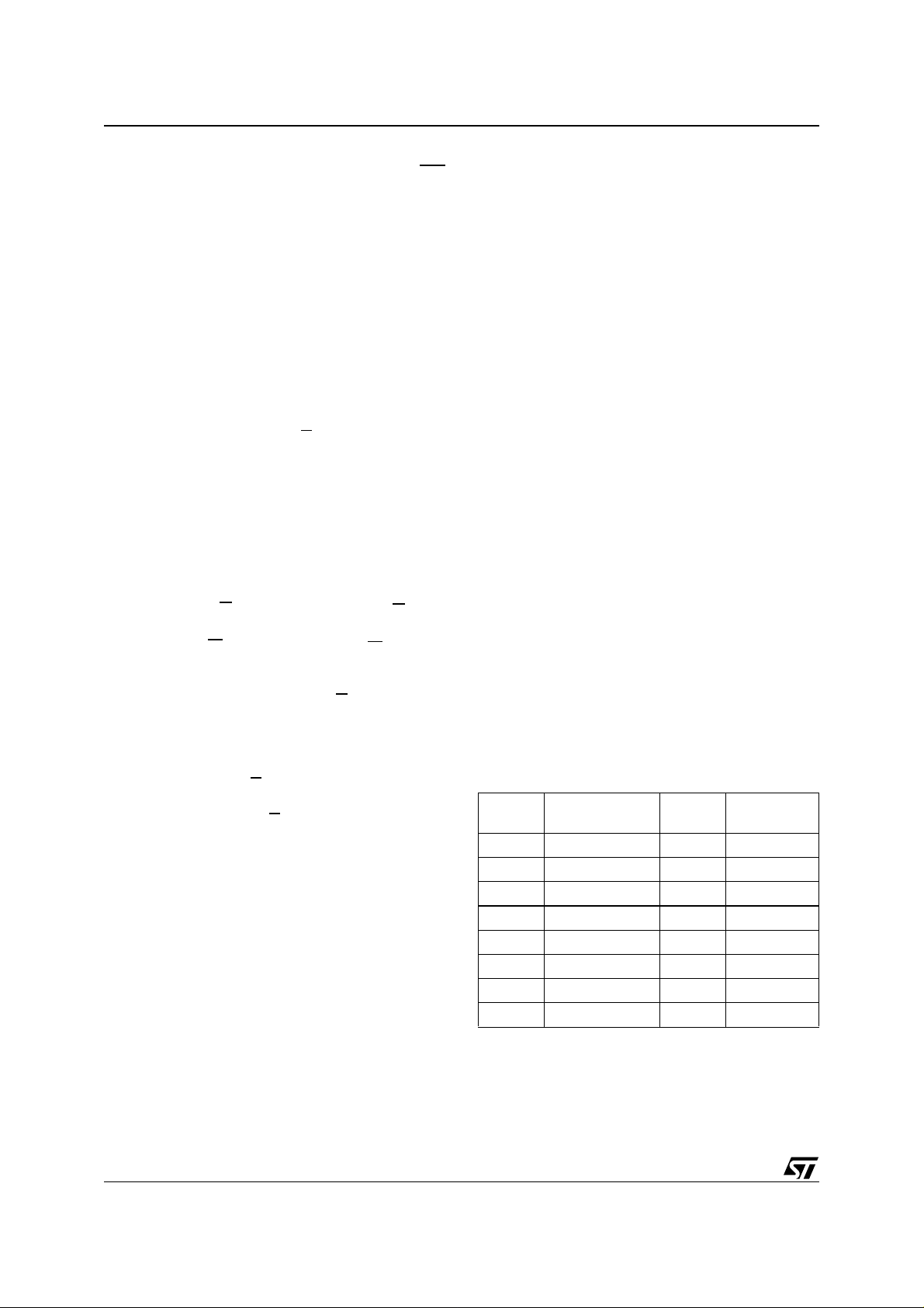
Table 3. Block Addresses
Size
(Kbytes)
64 70000h-7FFFFh 7 Top Block
64 60000h-6FFFFh 6 Main Block
64 50000h-5FFFFh 5 Main Block
,
64 40000h-4FFFFh 4 Main Block
64 30000h-3FFFFh 3 Main Block
64 20000h-2FFFFh 2 Main Block
64 10000h-1FFFFh 1 Main Block
64 00000h-0FFFFh 0 Main Block
Address Range
Block
Number
CC
CC
= VCC Pro-
will resu lt in
Block Type
10/41
Page 11

BUS OPERATIONS
The two interfaces have similar bus operations but
the signals and timings are completely different.
The Firmware Hub (FWH) Interface is the usual interface and all of the functionality of the part is
available through this interface. Only a subset of
functions are available through the Address/Address Multiplexed (A/A Mux) Interface.
Follow the section Firmware Hub (FWH) Bus Op-
erations below and the section Address/Address
Multiplexed (A/ A Mux) Bu s Operat ions be low for a
description of the bus operations on each interface.
Firmware Hub (FWH) Bus Operations
The Firmware Hub (FWH) Interface consists of
four data signals ( FWH0-FWH3), one control line
(FWH4) and a clock ( CLK). In addition protection
against accidental or malicious data corruption
can be achieved using two further signals (TBL
and WP). Finally two r eset signals (R P and INIT)
are available to put the memory into a known
state.
The data signals, contr ol signal and clock are de signed to be compatible with PCI electrical specifications. The interfa ce ope rates with c lock sp eeds
up to 33MHz.
The following operation s can be performed u sing
the appropriate bus cycles: Bus Read, Bus Write,
Standby, Reset and Block Protection.
Bus Read. Bus Read operations read from the
memory cells, speci fic registers in the Command
Interface or Firmware Hu b Registers. A va lid Bus
Read operation starts when Input Com mun icati on
Frame, FWH4, is Low, V
correct Start cycle is on FWH0-FWH3. On the fol lowing cloc k c ycl es t h e Host wi ll s en d t he M e mo ry
ID Select, Address and other control bits on
FWH0-FWH3. The memory respon ds by outputting Sync data until th e wait-states have elap sed
followed by Data0-Data3 and Data4-Data7.
Refer to Table 4., FWH Bus Read Field Defini-
tions, and Figure 7., FWH Bus Read Waveforms,
for a description of th e Field definitions for each
clock cycle of the transfer. See Table 20., FWH In-
terface AC Signal Timing Characteristics, and Figure 12., FWH Interface AC Signal Timing
Waveforms, for detai ls on the timings of the sig-
nals.
Bus Write. Bus Write operations write to the
Command Interface or Firmware Hub Registers. A
valid Bus Write op eration sta rts when I nput Communication Frame, FWH4, is Low, V
rises and the correct Start cycle is on FWH0FWH3. On the following Clock cycles the Host will
send the Mem ory ID Sel ect, Addres s, other co ntrol
bits, Data0-Data3 and Data4-Data7 on FWH0-
, as Clock rises and the
IL
, as Clock
IL
M50FW040
FWH3. The memory outpu ts Sync data until the
wait-states have elapsed.
Refer to Table 5., FWH Bus Write Field Defini-
tions, and Figure 8., FWH Bus Write Waveforms,
for a description of th e Field definitions for each
clock cycle of the transfer. See Table 20., FWH In-
terface AC Signal Timing Characteristics, and Figure 12., FWH Interface AC Signal Timing
Waveforms, for detai ls on the timings of the sig-
nals.
Bus Abort. The Bus Abort operation can be used
to immediately abort t he current b us operation. A
Bus Abort occurs w hen FWH 4 is driv en Low, V
during the bus operat ion; the memory will tr i-st ate
the Input/Output Communication pins, FWH0FWH3.
Note that, during a Bus Write operation, the Command Interface starts ex ecuting the comma nd as
soon as the data is fully received; a Bus Abort during the final TAR cycles is not guaranteed to abort
the command; the bus, however , will be releas ed
immediately.
Standby. When FWH4 is High, V
, the memory
IH
is put into Standby mode where FWH0-FWH3 are
put into a high-impedance state and the Supply
Current is reduced to the Standby level, I
Reset. During Reset mode all internal circuits are
switched off, the memory is deselected and the
outputs are put in high-impedance. The memory is
in Reset mode when Interface Reset, RP
Reset, INIT
Low, V
, is Low, VIL. RP or INIT must be he ld
, for t
IL
. The memory resets to Read
PLPH
mode upon return from Reset mode and the Lock
Registers return to their default state s regardless
of their state before Reset, see Table 10. If RP
goes Low, VIL, during a Program or Erase op-
INIT
eration, the operation is aborted and the mem ory
cells affected no longer contain valid data; the
memory can take up to t
to abort a Program
PLRH
or Erase operation.
Block Protection. Block Protection can be
forced usin g the sign als Top Bl ock Lo ck, TBL
Write Protect, W P
, regardless of th e state of the
Lock Registers.
Address/Address Multiplexed (A/A Mux) Bus
Operations
The Address/Address Multiplexed (A/A Mux) Interface has a more traditional style interface. The signals consist of a multiplexed addr ess si gna ls ( A0 A10), data signa ls, (DQ0-DQ7) and th ree control
signals (RC
, G, W). An additional signal, RP, can
be used to reset the memory.
The Address/Address Multiplexed (A/A Mux) Inter-
face is included for use by Flash Programming
equipment for faster fac tory prog ramming. O nly a
IL
.
CC1
, or CPU
or
, and
,
11/41
Page 12

M50FW040
subset of the features a vailable to the Firmware
Hub (FWH) Interface are available; these i nclude
all the Commands but exclude the Security features and other registers.
The following operation s can be performed u sing
the appropriate bus cycles: Bus Read, Bus Write,
Output Disable and Reset.
When the Address/Address Multiplexed (A/A Mux)
Interface is selec ted all the bloc ks are unprotect ed. It is not possible to protect any blocks through
this interface.
Bus Read. Bus Read operations are used to output the contents of the Memo ry Array, the Electronic Signature and the Status Register. A v alid
Bus Read operation begi ns by latching the Row
Address and Column Address signals into the
memory using the Address Inputs, A0-A10, and
the Row/Column Address Select RC
Enable (W
High, V
) and Interface Reset (RP) must be
, and Output Enable, G, Low, VIL, in order
IH
. Then Write
to perform a Bus Read operation. The Data Inputs/
Outputs will output the val ue, see Figure 14., A/A
Mux Interface Read AC Waveforms, and Table
22., A/A Mux Interface Read AC Charac teristics,
for details of when the output becomes valid.
Bus Write. Bus Write operations write to the
Command Interface. A valid Bus Write operati on
begins by latching the Ro w Address and C olumn
Address signals into the memory using the Address Inputs, A0-A10, and the Row/Column Address Select RC
Data Inputs/Outputs; Output Enable, G
face Reset, RP
able, W
, must be Low, VIL. The Data Inputs/
. The data should be set up on the
, and Inter-
, must be High, VIH and Write En-
Outputs are latched on the rising edge of Write Enable, W
. See Figure 15., A/A Mux Interface Write
AC Waveforms, and Ta ble 23 ., A/A Mux In terfac e
Write AC Characteristi cs, for details of the timing
requirements.
Output Disable. The data outputs are high-im-
pedance when the Output Enable, G
, is at VIH.
Reset. During Reset mode all internal circuits are
switched off, the memory is deselected and the
outputs are put in high-impedance. The memory is
in Reset mode when RP
held Low, V
IL
for t
PLPH
is Low, VIL. RP must be
. If RP is goes Low, VIL, during a Program or Erase operation, the operation is
aborted and the me mory cells affected no longer
contain valid data; the memory can take up to t
to abort a Program or Erase operation.
RH
Table 4. FWH Bus Read Field Definitions
Clock
Cycle
Number
3-9 7 ADDR XXXX I
10 1 MSIZE 0000b I Always 0000b (only single byte transfers are supported).
11 1 TAR 1111b I The host drives FWH0-FWH3 to 1111b to indicate a turnaround cycle.
12 1 TAR
13-14 2 WSYNC 0101b O
15 1 RSYNC 0000b O
16-17 2 DATA XXXX O
18 1 TAR 1111b O
19 1 TAR
Clock
Cycle
Count
1 1 START 1101b I
2 1 IDSEL XXXX I
Field
FWH0-
FWH3
1111b
(float)
1111b
(float)
Memory
N/A
I/O
On the rising edge of CLK with FWH4 Low, the contents of FWH0FWH3 indicate the start of a FWH Read cycle.
Indicates which FWH Flash Memory is selected. The value on FWH0FWH3 is compared to the IDSEL strapping on the FWH Flash
Memory pins to select which FWH Flash Memory is being addressed.
A 28-bit a ddre ss phas e i s t rans ferr ed s t art ing wit h t he m ost si gni fic ant
nibble first.
The FWH Flash Memory takes control of FWH0-FWH3 during this
O
cycle.
The FWH Flash Memory drives FWH0-FWH3 to 0101b (short wait-
sync) for two clock cycles, indicating that the data is not yet available.
Two wait-states are always included.
The FWH Flash Memory drives FWH0-FWH3 to 0000b, indicating
that data will be available during the next clock cycle.
Data transfer is two CLK cycles, starting with the least significant
nibble.
The FWH Flash Memory drives FWH0-FWH3 to 1111b to indicate a
turnaround cycle .
The FWH Flash Memory floats its outputs, the host takes control of
FWH0-FWH3.
Description
PL-
12/41
Page 13

Figure 7. FWH Bus Read Waveforms
CLK
FWH4
M50FW040
FWH0-FWH3
Number of
clock cycles
START IDSEL ADDR MSIZE TAR SYNC DATA TAR
11712322
Table 5. FWH Bus Write Field Definitions
Clock
Cycle
Number
1 1 START 1110b I
2 1 IDSEL XXXX I
3-9 7 ADDR XXXX I
10 1 MSIZE 0000b I Always 0000b (single byte transfer).
11-12 2 DATA XXXX I
13 1 TAR 1111b I
14 1 TAR
15 1 SYNC 0000b O
16 1 TAR 1111b O
17 1 TAR
Clock
Cycle
Count
Field
FWH0-
FWH3
1111b
(float)
1111b
(float)
Memory
I/O
O
N/A
Description
On the rising edge of CLK with FWH 4 Lo w, the contents of
FWH0-FWH3 indica te the start of a FWH Write Cyc le.
Indicates which FWH Flash Memory is selected. The value
on FWH0-FWH3 is compared to the IDSEL strapping on the
FWH Flash Memory pins to select which FWH Flash
Memory is being address ed .
A 28-bit address phase is transferred starting with the most
significant nibble first.
Data transfer is two cycles, starting with the least significant
nibble.
The host drives FWH0-FWH3 to 1111b to indicate a
turnaround cycle.
The FWH Flash Memory takes contr ol of FW H0 -F WH 3
during this cycle.
The FWH Flash Memory drives FWH0-FWH3 to 0000b,
indicating it has received data or a command.
The FWH Flash Memory drives FWH0-FWH3 to 1111b,
indicating a turnaround cycle.
The FWH Flash Memory floats its outputs and the host takes
control of FWH0-FWH3.
AI03437
Figure 8. FWH Bus Write Waveforms
CLK
FWH4
FWH0-FWH3
Number of
clock cycles
START IDSEL ADDR MSIZE DATA TAR SYNC TAR
11712212
AI03441
13/41
Page 14

M50FW040
COMMAND INTERFACE
All Bus Write operations to the memory are interpreted by the Command Interface. Commands
consist of one or more sequential Bus Write operations.
After power-up or a Reset operation the mem ory
enters Read mode.
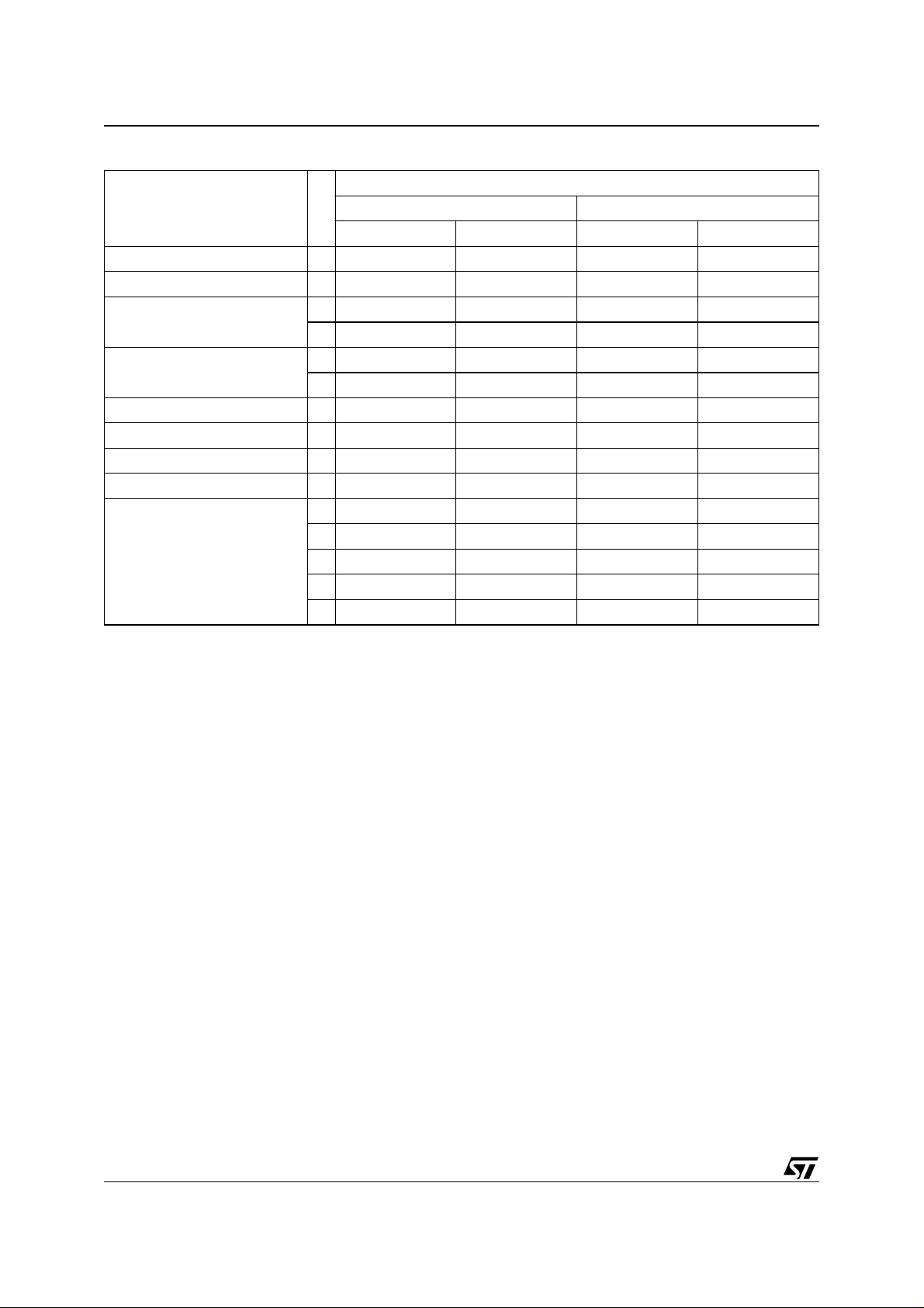
The commands are summarized in Table
7., Commands. Refer to Table 7. in conjunction
with the text descriptions below.
Read Memory Array Command. The Read Mem-
ory Array command returns the memory to its
Read mode where it behaves like a ROM or
EPROM. One Bus Writ e cycle is required to issue
the Read Memory Array command and re turn the
memory to Read mode. Onc e the c ommand i s issued the memory remai ns in Read mode until another command is issued. F rom Read mode Bus
Read operations will access the memory array.
While the Program/Erase Controller is executing a
Program or Erase ope ration the memory will not
accept the Read Memory Array command until the
operation completes.
Read Status Register Command. The Read Status Register command is us ed to read th e Status
Register. One Bus Write cycle is required to issue
the Read Status Register command. Once the
command is issued s ubseq uent Bu s Read ope rations read the Statu s Register until a nother command is issued. See the section on the Status
Register for details on the definitions of the Status
Register bits.
Read Electronic Signature C omma nd. The Read
Electronic Signature command is used to read the
Manufacturer Code and the Device Code. One
Bus Write cycle is required to issue the Read Electronic Signature command. Once the command is
issued subsequent B us Re ad o per at ion s read the
Manufacturer Code or the D evice Code until another command is issued.
After the Read Electronic Signature Command is
issued the Manufactur er Code and Device Code
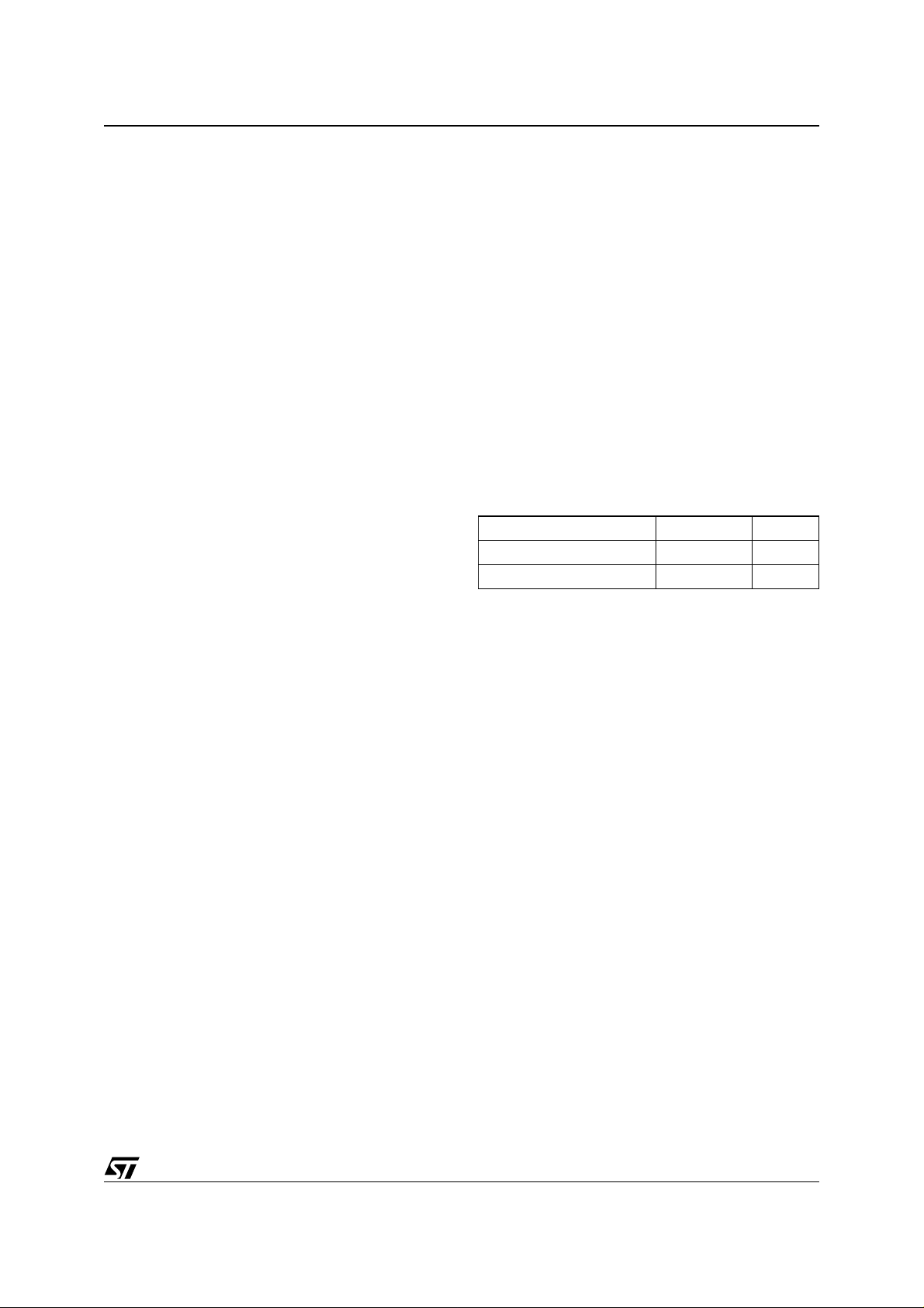
can be read using Bus Read ope ra tio ns usi ng the
addresses in Table 6.
Program Command. The Program command
can be used to program a value to one address in
the memory array at a time. Two Bus Write operations are required to issue t he co mma nd; the sec ond Bus Write cycle latches the address and data
in the internal state machine and starts the Program/Erase Controller. Once the command is issued subsequent Bus Read operations read the
Status Register. See the section on the Status
Register for details on the definitions of the Status
Register bits.
If the address falls in a protect ed block then the
Program operation will abort, the data in the memory array will not be changed and the Stat us Reg ister will output the error.
During the Program operation the memory will
only accept the R ead Status Register command
and the Program/Erase Suspend command. All
other commands will be igno re d. Typ ical P ro gr am
times are given in Table 12.
Note that the Program command cannot change a
bit set at ‘0’ back to ‘1’ and attempting to do so will
not cause any modification on its value. The Erase
command must be used to set all of the bits in the
block to ‘1’.
See Figure 19., Program Flowchart and Pseudo
Code, for a suggested flowchart on using the Pro-
gram command.
Erase Command. The Erase command can be
used to erase a block. T wo Bus Write oper ations
are required to issue the command; the second
Bus Write cycle latches the block address in the internal state machine and starts the Program/Erase
Controller. Once the command is issued subsequent Bus Read opera tions read th e Status Reg ister. See the section on the S tatus Register for
details on the definitions of the Status Register
bits.
If the block is protected then the Erase oper ation
will abort, the data in the block will not be changed
and the Status Register will output the error.
During the Erase oper ation the memory will onl y
accept the Read Status Register command and
the Program/Erase Suspe nd command. All other
commands will be ignored. Typical Erase times
are given in Table 12.
The Erase command sets all of the bits in the block
to ‘1’. All previous data in the block is lost.
See Figure 21., Erase Flowchart and Pseudo
Code, for a suggested flowchart on using the
Erase command.
Clear Status Register Command. The Clear Sta-
tus Register command can be used to reset bits 1,
3, 4 and 5 in the Status Register to ‘0’. O ne Bus
Write is required to issue the Clear Status Register
command. Once the command is issued the memory returns to its pr evious mod e, subseq uent Bus
Read operations continue to output the same data.
The bits in the Status Register are sticky and do
not automatically return to ‘0’ when a new Program
or Erase command is issued. If an error occurs
then it is essential to clear any error bits in the Status Register by issuing the Clear Status Register
command before attempting a new Program or
Erase command.
14/41
Page 15
M50FW040
Program/Erase Suspend Command. The Pro-
gram/Erase Suspend command can be used to
pause a Program or Erase operation. One Bus
Write cycle is required to issue the Program/Erase
Suspend command and pause the Program/Erase
Controller. Once the comm and is issue d it i s necessary to poll the Program/Erase Controller Status
bit to find out when the Program /Erase Control ler
has paused; no other commands will be accepted
until the Program/Erase Controller has paused.
After the Program/Erase Controller has paused,
the memory will continue to output the Status Register until another command is issued.
During the polling period between issuing the Program/Erase Suspend command and the Program/
Erase Controller pa using it i s possib le for the op eration to complete. Once Program/Erase Controller Status bit indicates that the Program/Erase
Controller is no longer active, the Program Suspend Status bit or the Erase Suspen d Status bit
can be used to determine if the operation has completed or is suspended. For timing on the delay between issuing the Program/Erase Suspend
command and the Program/Erase Controller
pausing see Table 12.
During Program/Erase S usp end th e Read Memory Array, Read Statu s Register, Read El ectronic
Signature and Program/Erase Resume commands will be accepted by the Command Interface. Additionally, if the su spe nde d operation was
Erase then the Program command will also be accepted; only the blocks not being erased may be
read or programmed correctly.
See Figure 20., Program Suspend & Resume
Flowchart and Pseudo Code, and Figure
22., Erase Suspend & Resume Flowchart and
Pseudo Code, for sug gested flowcharts on using
the Program/Erase Suspend command.
Program/Erase Resume Command. The Pro-
gram/Erase Resume command can be used to restart the Program/Erase Controller after a
Program/Erase S us pen d o perati on has paused it.
One Bus Write cyc le is required to issue the P rogram/Erase Resume command. Once the command is issued subsequent Bus Read operations
read the Status Register.
Table 6. Read Electronic Signature
Code Address Data
Manufacturer Code 00000h 20h
Device Code 00001h 2Ch
15/41
Page 16
M50FW040
Table 7. Commands
Bus Write Operations
Command
Cycles
Address Data Address Data
Read Memory Array 1 X FFh
Read Status Register 1 X 70h
1 X 90h
Read Electronic Signature
1 X 98h
2 X 40h PA PD
Program
2 X 10h PA PD
Erase 2 X 20h BA D0h
Clear Status Register 1 X 50h
Program/Erase Su spe nd 1 X B0h
Program/Erase Re sum e 1 X D0h
1 X 00h
1 X 01h
Invalid/Reserved
1 X 60h
1X 2Fh
1X C0h
Note: X Don’t Care, PA Program Address, PD Program Data, BA Any ad dress in the Block.
Read Memory Array. After a Read Memory Array command, read the memory as normal until another command is issued.
Read Status Register. A fter a Read St atus Regist er command, read the St atus Registe r as normal until ano th er command is issued.
Read Elec t ro n i c Signatur e. After a Read Electronic Signature command, read Manufacturer Code, Device Code until another com-
mand is issued.
Erase, Program. After these commands read t he Status Register until the command completes and another command is issued.
Clear Status Register. After the Clear Status Register command bits 1, 3, 4 and 5 in the Status Register are reset to ‘ 0’.
Program/Erase Suspend. After the Program/Erase Suspend command has been accepted, issue Read Memory A rray, Read Status
Register, Program (during Erase suspend) and Program/Erase resume commands.
Program/Er ase Resu me. After the Program/Erase Resume command the suspended Program/Erase operation resumes, read the
Status Register until the Program/Erase Controller completes and the memory returns to Read Mode.
Invalid/Reserved. Do not use Invalid or Reserved commands.
1st 2nd
16/41
Page 17

STATUS REGISTER
The Status Register p rovides information on the
current or previo us Program or Erase operati on.
Different bits in the Status Register con vey differ ent information and errors on the operation.
To read t he St a t us R egister the R ead St a t us R egister command can be issued. The Status Register
is automatically read after Program, Erase and
Program/Erase Resume commands are issued.
The Status Register can be read from any address.
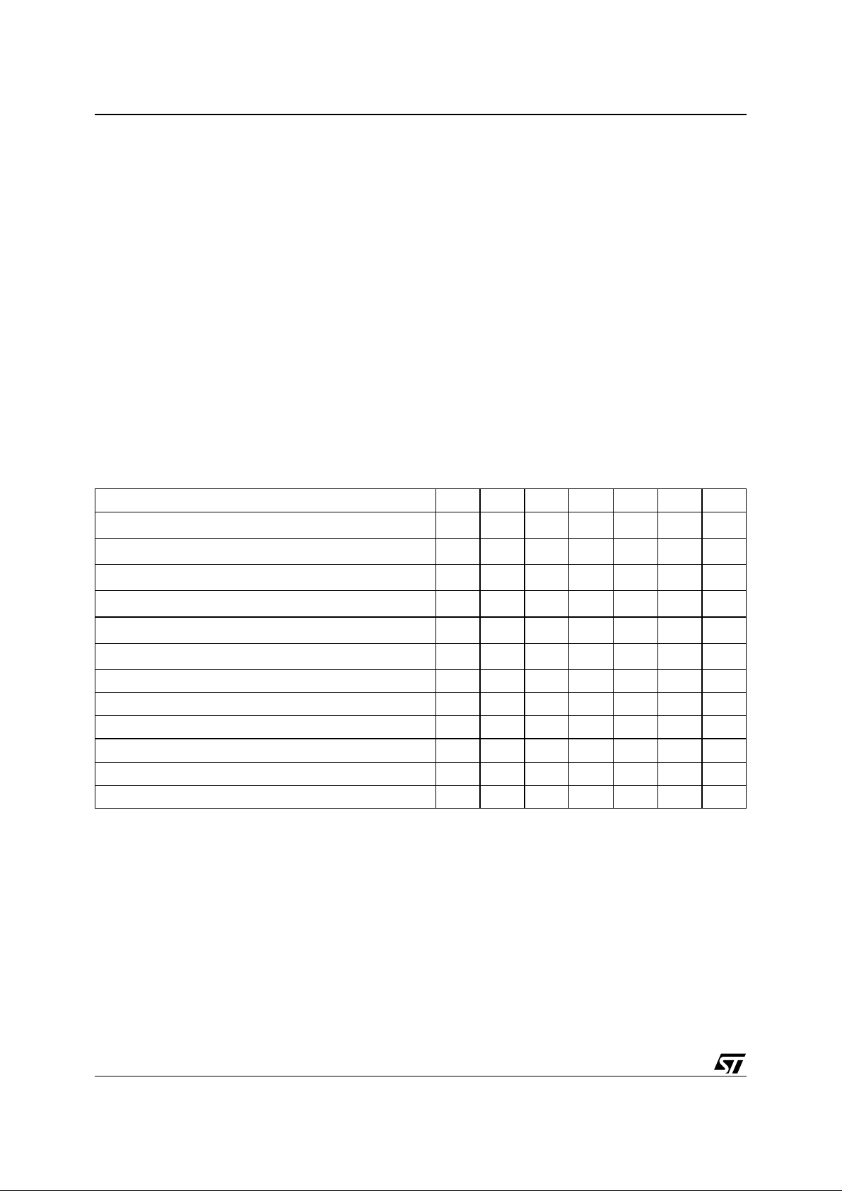
The Status Register bits are summarized in Status
Register Bits. Refer to Table 8. in conjunct ion wit h
the text descriptions below.
Program/Erase Controller Status (Bit 7). The Pro-
gram /Erase Controller Status bit indicates whether
the Program/Erase Controller is active or inactive.
When the Program/Eras e Controller Status bit is
‘0’, the Program/Eras e Controller is active; when
the bit is ‘1’, the Program/Erase Controller is inactive.
The Program/Erase Con troller Status is ‘0 ’ immediately after a Program/E rase Sus pend co mmand
is issued until the Program/Erase Controller pauses. After the Program/Erase Controller pauses the
bit is ‘1’.
During Program and Erase operation the Program/Erase Controller Statu s bit can be polled to
find the end of the op er ation. T he othe r bit s in the
Status Register should not be tested until the Program/Erase Controller completes the operation
and the bit is ‘1’.
After the Program/Eras e Controller completes its
operation the Erase S tatus, Program Status , V
Status and Block Protecti on Statu s bits sh ould be
tested for errors.
Erase Suspend Status (Bit 6). The Erase Suspend Status bit indica tes that an Erase op eration
has been suspended and is waiting to be resumed. The Erase Suspend Status should only be
considered valid when the Program/Erase Controller Status bit is ‘1’ (Program/Erase Controller
inactive); after a Program/Erase Suspend command is issued the memory may still complete the
operation rather than entering the Suspend mode.
When the Erase Suspend Status bit is ‘0’ the Program/Erase Controller i s active or has comp leted
its operation; when the b it is ‘1’ a Program /Erase
Suspend command has been issued and the
memory is waiting for a Progr am/Erase Resume
command.
When a Program/Erase Res ume command is issued the Erase Suspend Status bit returns to ‘0’.
Erase Status (Bit 5). The Erase Status bit ca n be
used to identify if the memory has applied the
maximum number of erase pulses to the block and
PP
M50FW040
still failed to verify that the block has erased correctly. The Erase Statu s bit should be read once
the Program/Erase Controller Status bit is ‘1’ (Program/Erase Controller inactive).
When the Erase Status bit is ‘0’ the memo ry has
successfully verified that the block has erased correctly; when the Erase Status bit is ‘1’ the Program/Erase Controller has applied the maximum
number of pulses to the block and still failed to verify that the block has erased correctly.
Once the Erase Status bit i s set to ‘1’ the it can
only be reset to ‘0’ by a Clear Status Register command or a hardware reset. If it is set to ‘1’ it should
be reset before a new Program or Erase command
is issued, otherwise the new command will appear
to fail.
Program Status (Bit 4). The Progr am Status bit
can be used to i dentify if the me mory ha s app lied
the maximum number of program pulses to the
byte and still failed to ve rify tha t the byte has p rogrammed correctly. The Program Status bit should
be read once the Program/Erase Controller Status
bit is ‘1’ (Program/Erase Controller inactive).
When the Program Status bit is ‘0’ the memory has
successfully verified that the byte has programmed correctly; when the Program Status bit is
‘1’ the Program/Erase Controller has applied the
maximum number of pulses to the byte and still
failed to verify that the by te has program med c orrectly.
Once the Program Status bit is set to ‘1’ it can only
be reset to ‘0’ by a Clear Status Register command or a hardware reset. If it is set to ‘1’ it should
be reset before a new Program or Erase command
is issued, otherwise the new command will appear
to fail.
V
Status (Bit 3). The VPP Status bit can be
PP
used to identify an invalid v oltage on the V
during Program and Erase operations. The V
pin is only sampled at the beginning of a Program
or Erase operation. Indeterminate res ults can oc cur if V
becomes invalid during a Program or
PP
Erase operation.
When the V
V
pin was sampled a t a valid voltage; when the
PP
Status bit is ‘1’ the VPP pin has a voltage that
V
PP
is below the V
Status bit is ‘0’ the voltage on the
PP
Lockout Voltage, V
PP
memory is protected; Program and Erase operation cannot be performed.
Once the V
Status bit set to ‘1’ it can only be re-
PP
set to ‘0’ by a Clear Status Register command or a
hardware reset. If it is set to ‘1’ i t should be res et
before a new Program or Eras e command is issued, otherwise the new command will appea r to
fail.
PPLK
PP
, the
pin
PP
17/41
Page 18
M50FW040
Program Suspend Status (Bit 2). The Program
Suspend S t atu s bit indica te s t hat a Pr og r a m o pe ration has been suspended and is waiting to be resumed. The Program Suspend Status should only
be considered valid when the Program/Erase
Controller Status bit is ‘1’ (Program/Erase Controller inactive); after a Program/Erase Suspend command is issued the memory may still complete the
operation rather than entering the Suspend mode.
When the Program S uspend Status bit is ‘0’ the
Program/Erase Controller is active or has completed its operation; when the bit is ‘1’ a Program/
Erase Suspend command has been issued and
the memory is waiting for a Program/Erase Resume command.
When a Program/Erase Res ume command is issued the Program S uspend Status bit returns to
‘0’.
gram or Erase operation has tried to modify the
contents of a protected block. When the Block Protection Status bit is to ‘0’ no Program or Erase operations have been a ttem pte d to pr ote cted blocks
since the last Cle ar Status Register command or
hardware reset; when the B lock Pro tec tio n Status
bit is ‘1’ a Program or Erase operation has been attempted on a protected block.
Once it is set to ‘1’ the Block Prot ection Status bit
can only be reset to ‘0’ by a Clear Status Register
command or a hardware reset. If it is set to ‘1’ it
should be reset before a new Pro gram or Erase
command is issu ed, othe rwise the new comma nd
will appear to fail.
Using the A/A Mux Interface the B lock Protecti on
Status bit is always ‘0’.
Reserved (Bit 0). Bit 0 of the Status Register i s
reserved. Its value should be masked.
Block Protection Status (Bit 1). The Block Protection Status bit can be used to identify if the Pro-
Table 8. Status Register Bits
Operation Bit 7 Bit 6 Bit 5 Bit 4 Bit 3 Bit 2 Bit 1
(1)
Program active ‘0’
Program suspended ‘1
Program completed successfully ‘1’
Program failure due to V
Program fa i lu r e du e t o B lo c k P r ot ect i on ( FW H I n te r fa c e o n ly ) ‘1’
Program failure due to cell failure ‘1’
Erase active ‘0’ ‘0’ ‘0’ ‘0’ ‘0’ ‘0’ ‘0’
Erase suspended ‘1’ ‘1’ ‘0’ ‘0’ ‘0’ ‘0’ ‘0’
Erase completed successfully ‘1’ ‘0’ ‘0’ ‘0’ ‘0’ ‘0’ ‘0’
Erase failure due to V
Erase failure due to Block Protection (FWH Interface only) ‘1’ ‘0’ ‘0’ ‘0’ ‘0’ ‘0’ ‘1’
Erase failure due to failed cell(s) in block ‘1’ ‘0’ ‘1’ ‘0’ ‘0’ ‘0’ ‘0’
Note: 1. For Program operations during Erase Suspend Bit 6 is ‘ 1’, otherwise Bit 6 is ‘0’.
PP
Error
PP
Error
X
X
X
‘1’
X
X
X
‘1’ ‘0’ ‘0’ ‘0’ ‘1’ ‘0’ ‘0’
‘0’ ‘0’ ‘0’ ‘0’ ‘0’
(1)
‘0’ ‘0’ ‘0’ ‘1’ ‘0’
(1)
‘0’ ‘0’ ‘0’ ‘0’ ‘0’
(1)
‘0’ ‘0’ ‘1’ ‘0’ ‘0’
(1)
‘0’ ‘0’ ‘0’ ‘0’ ‘1’
(1)
‘0’ ‘1’ ‘0’ ‘0’ ‘0’
18/41
Page 19

FIRMWARE HUB (FWH) INTERFACE CONFIGURATION REGISTERS
When the Firmware Hub Interface is selected several additional registe rs can be accessed. These
registers control the protection status of the
Blocks, read the Gener al Purpose Input pins and
identify the memory using the Electronic Signature
codes. See Table 9. for the memory map of the
Configuration Registers.
Lock Registers
The Lock Registers control the protection status of
the Blocks. Each Block has its own Lock Register.
Three bits within each L ock Register control the
protection of each block, the Write Lock Bit, the
Read Lock Bit and the Lock Down Bit.
The Lock Registers can be read and written,
though care should be taken when writing as, once
the Lock Down Bit is set, ‘1’, f urther modi fication s
to the Lock Register cannot be made until cleared,
to ‘0’, by a reset or power-up.
See Table 1 0. for details on the bit definiti ons of
the Lock Registers.
Write Lock. The Write Lock Bit determines
whether the contents of the Block can be modified
(using the Program or Erase Command). When
the Write Lock Bit is set, ‘1’, the block is write protected; any operations tha t attempt to c hange the
data in the block will fai l and the Status Register
will report t he e rror. When the Wr it e Lo ck Bi t is reset, ‘0’, the block is not write protected through the
Lock Register and may be modified unless write
protected through some other means.
When V
is less than V
PP
all blocks are pro-
PPLK
tected and cannot be m odified, regardless of the
state of the Write Lock Bit. If Top Block Lock, TBL
is Low, V
, then the Top Block (Block 7) is write
IL
protected and cannot be modified. Similarly, if
Write Protect, WP
, is Low, VIL, then the Main
Blocks (Blocks 0 to 6) are write protected and cannot be modified.
After power-up or reset the Write Lock Bit is always set to ‘1’ (write protected).
Read Lock. The Read Lock bit determines
whether the contents of the Block can be read
(from Rea d mode). When the Re ad Lo ck Bit is set ,
‘1’, the block is read protecte d; any ope ration t hat
attempts to read the contents of the block will read
00h instead. When the Re ad Loc k B it is r es et, ‘0 ’,
read operations in the Blo ck return the data programmed into the block as expected.
After power-up or reset the Read Lock Bit is always reset to ‘0’ (not read protected).
Lock Down. The Lock Down Bit provides a
mechanism for protecting softwa re data from sim -
ple hacking and malicious a ttack. When the Lock
Down Bit is set, ‘1’, further modification to the
Write Lock, Read Lock and Lock Down Bits cannot
be performed. A reset or power-u p is requ ired before changes to these bits can be made. When the
Lock Down Bit is reset, ‘0’ , the Write Lock, Read
Lock and Lock Down Bits can be changed.
Firmware Hub (FWH) General Purpose Input
Register
The Firmware Hub (FWH ) General Purp ose Input
Register holds the state of the Firmware Hub Interface General Purpose Input pins, FGPI0-FGPI4.
When this register is read, the state of these pins
is returned. This register is read-only and writing to
it has no effect.
The signals on the Firmware Hub Interface General Purpose Input pins should remain constant
throughout the whole Bus Rea d cycle in order to
guarantee that the correct data is read.
Manufacturer Code Register
Reading the Manufacture r Code Register returns
the manufacturer code for the memor y. The man ufacturer code for STMicroelectronics is 20h. This
register is read-only and writing to it has no effect.
Device Code Register
Reading the Device Code Register returns the device code for the memory, 2Ch. This register is
read-only and writing to it has no effect.
Firmware Hub (FWH) General Purpose Input
Register
The Firmware Hub (FWH ) General Purp ose Input
Register holds the state of the Firmware Hub Inter-
,
face General Purpose Input pins, FGPI0-FGPI4.
When this register is read, the state of these pins
is returned. This register is read-only and writing to
it has no effect.
The signals on the Firmware Hub Interface General Purpose Input pins should remain constant
throughout the whole Bus Rea d cycle in order to
guarantee that the correct data is read.
Manufacturer Code Register
Reading the Manufacture r Code Register returns
the manufacturer code for the memor y. The man ufacturer code for STMicroelectronics is 20h. This
register is read-only and writing to it has no effect.
Device Code Register
Reading the Device Code Register returns the device code for the memory, 2Ch. This register is
read-only and writing to it has no effect.
M50FW040
19/41
Page 20
M50FW040
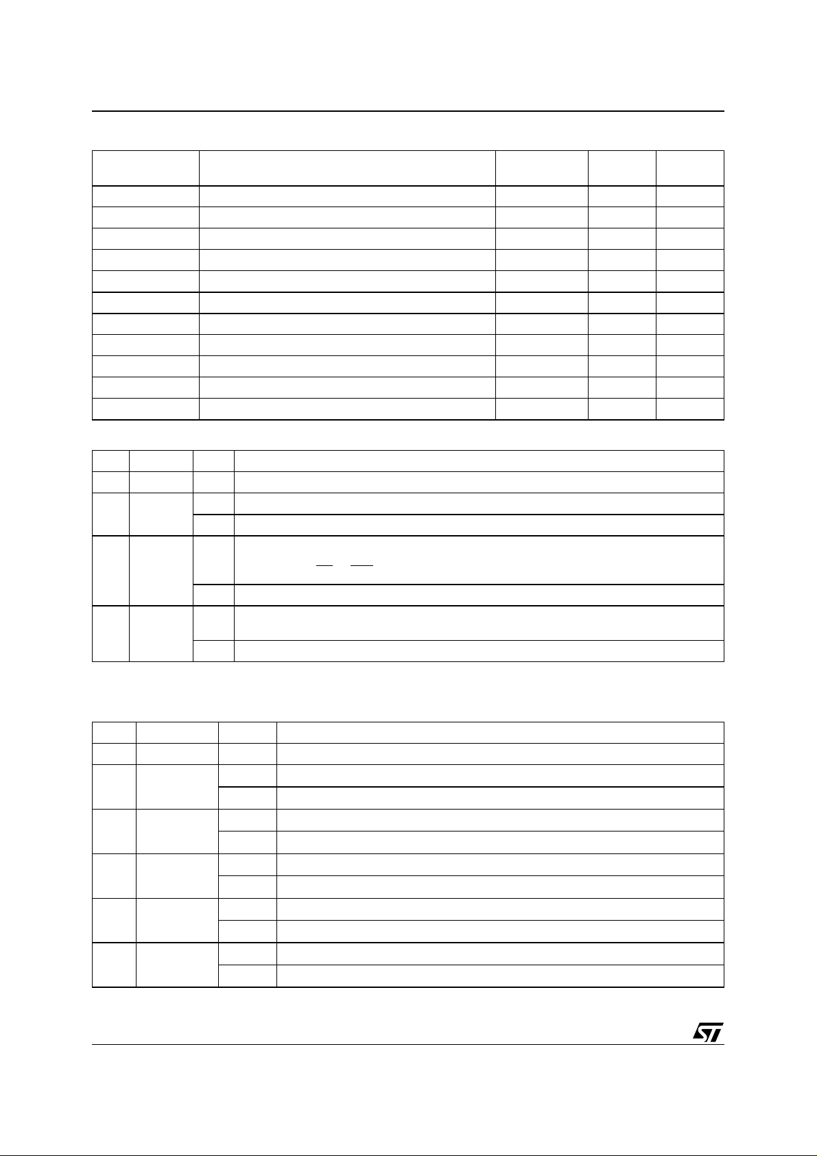
Table 9. Firmware Hub Register Configuration Map
Mnemonic Register Name
Memory
Address
T_BLOCK_LK Top Block Lock Register (Block 7) FBF0002h 01h R/W
T_MINUS01_LK Top Block [-1] Lock Register (Block 6) FBE0002h 01h R/W
T_MINUS02_LK Top Block [-2] Lock Register (Block 5) FBD0002h 01h R/W
T_MINUS03_LK Top Block [-3] Lock Register (Block 4) FBC0002h 01h R/W
T_MINUS04_LK Top Block [-4] Lock Register (Block 3) FBB0002h 01h R/W
T_MINUS05_LK Top Block [-5] Lock Register (Block 2) FBA0002h 01h R/W
T_MINUS06_LK Top Block [-6] Lock Register (Block 1) FB90002h 01h R/W
T_MINUS07_LK Top Block [-7] Lock Register (Block 0) FB80002h 01h R/W
FGPI_REG Firmware Hub (FWH) General Purpose Input Register FBC0100h N/A R
MANUF_REG Manufacturer Code Register FBC0000h 20h R
DEV_REG Device Code Register FBC0001h 2Ch R
Table 10. Lock Register Bit Definitions
Bit Bit Name Value Function
7-3 Reserved
2 Read-Lock
1 Lock-Down
0 Write-Lock
Note: 1. Applies to Top Block Lock Register (T_BLOCK_LK ) and Top Block [-1] Lock Regis ter (T_MINUS01_ LK) to Top Block [-7 ] Lock Reg-
ister (T_MINUS07_LK).
‘1’ Bus Read operations in this Block always return 00h.
‘0’ Bus read operations in this Block return the Memory Array contents. (Default value).
Changes to the Read-Lock bit and the Write-Lock bit cannot be performed. Once a ‘1’ is
‘1’
written to the Lock-Down bit it cannot be cleared to ‘0’; the bit is always reset to ‘0’ following
a Reset (using RP
or INIT) or after power-up.
‘0’ Read-Lock and Write-Lock can be changed by writing new values to them. (Default value).
Program and Erase operations in thi s Block will set an error in the Status Register. The
‘1’
memory contents will not be changed. (Default value).
‘0’ Program and Erase oper at i on s in t hi s Bl oc k ar e e xe cu t ed an d w i ll m od if y t he Bl oc k co nt en ts.
Default
Value
Access
Table 11. General Purpose Inputs Register Definition
Bit Bit Name Value Function
7-5 Reserved
Input Pin FGPI4 is at V
4 FGPI4
3 FGPI3
2 FGPI2
1 FGPI1
0 FGPI0
Note: 1. Applies to the General Purpose Inputs Register (FGPI-REG).
Input Pin FGPI4 is at V
‘0’
Input Pin FGPI3 is at V
‘1’
Input Pin FGPI3 is at V
‘0’
Input Pin FGPI2 is at V
‘1’
Input Pin FGPI2 is at V
‘0’
Input Pin FGPI1 is at V
‘1’
Input Pin FGPI1 is at V
‘0’
Input Pin FGPI0 is at V
‘1’
Input Pin FGPI0 is at V
‘0’
20/41
‘1’
IH
IL
IH
IL
IH
IL
IH
IL
IH
IL
Page 21
M50FW040
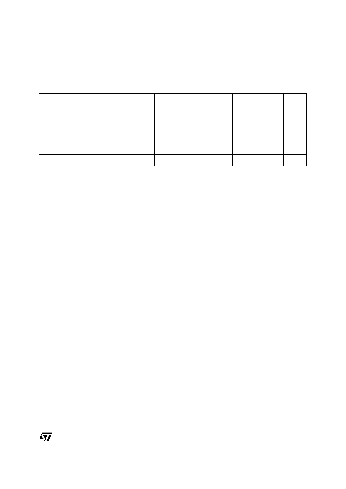
PROGRAM AND ERASE TIMES
The Program and Erase times are shown in Table
12.
Table 12. Program and Erase Times
Parameter Test Condition Min
Byte Program 10 200 µs
Block Program 0.4 5 sec
V
= 12V ± 5%
Block Erase
PP
= V
V
PP
CC
Program/Erase Suspend to Program pause(2) 5 µs
Program/Erase Suspend to Block Erase pause
Note: 1. TA = 25°C, VCC = 3.3V
2. Sampled only, not 100% tested.
(2)
Typ
(1)
Max Unit
0.75 8 sec
110sec
30 µs
21/41
Page 22
M50FW040
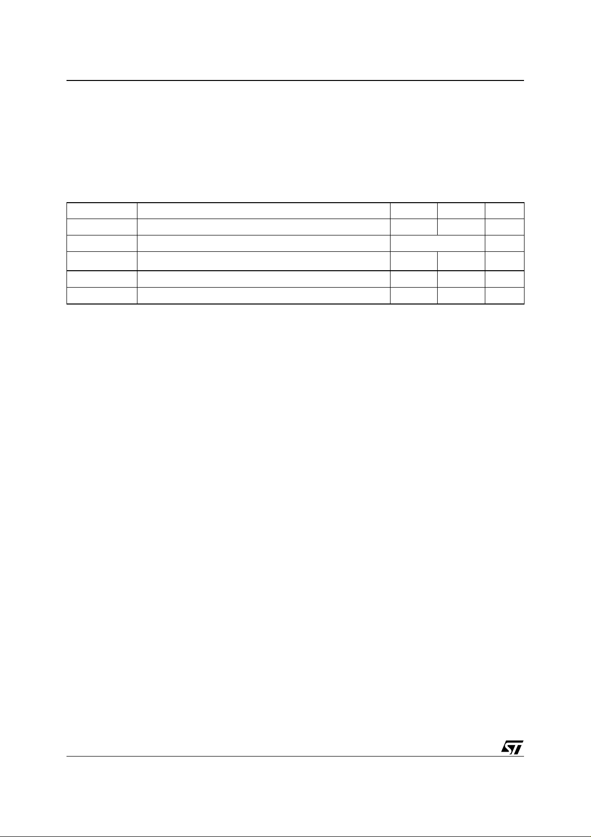
MAXIMUM RATING
Stressing the device above the ra ting l isted in the
Absolute Maximum Ratin gs table ma y cause per manent damage to the device. Thes e are stress
ratings only and operation of the device at these or
any other conditions abo ve those indica ted in the
Operating sections of this specification is not im-
Table 13. Absolute Maximum R atings
Symbol Parameter Min Max Unit
T
STG
T
LEAD
(2)
V
IO
V
CC
V
PP
Note: 1. Compliant with JEDEC Std J-STD-020B (for small body, Sn-Pb or Pb as sembly), the ST ECOPACK ® 7191395 specificat ion, and
the European directive on Restric tions on Hazardous Substances (RoHS) 2002/95/EU.
2. Minimum Voltage may undershoot to –2V and f or less than 20ns during transitions. Maximum Voltage may overshoot to V
and for less than 20ns during trans itions.
Storage Temperature –65 150 °C
Lead Temperature during Soldering See note 1 °C
Input or Output Voltage –0.6
Supply Voltage –0.6 4 V
Program Voltage –0.6 13 V
plied. Exposu re to Abso lute Max imum Rati ng conditions for extended periods may affect device
reliability. Refer also to the STMicroelectronics
SURE Program and o ther relevant quality documents.
V
CC
+ 0.6
CC
V
+2V
22/41
Page 23
M50FW040
DC AND AC PARAMETERS
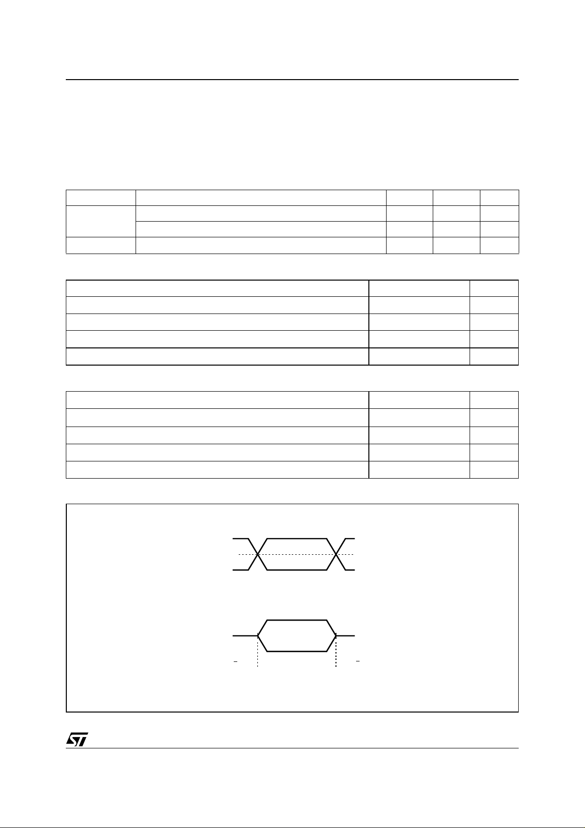
This section summ arizes the operating measurement conditions, and th e DC and AC c haracteris tics of the device. The parameters in the DC and
AC characteristics Tables that follow, are derived
from tests performed under the Measurement
Table 14. Operating Conditions
Symbol Parameter Min Max Unit
T
A
V
CC
Ambient Operating Temperature (Device Grade 1) 0 70 °C
Ambient Operating Temperature (Device Grade 5) –20 85 °C
Supply Voltage 3 3.6 V
Table 15. FWH Interface AC Measurement Conditions
Parameter Value Unit
Load Capacitance (C
Input Rise and Fall Times ≤ 1.4 ns
Input Pulse Voltages
Input and Output Timing Ref. Voltages
)
L
Conditions summarized in Table 14., Table 15.
and Table 16. Designers should check that the operating conditions in their circuit match the operating conditions when relying on the quoted
parameters.
10 pF
0.2 V
and 0.6 V
CC
0.4 V
CC
CC
V
V
Table 16. A/A Mux Interface AC Measurement Conditions
Parameter Value Unit
Load Capacitance (C
)
L
30 pF
Input Rise and Fall Times ≤ 10 ns
Input Pulse Voltages 0 to 3 V
Input and Output Timing Ref. Voltages 1.5 V
Figure 9. FWH Interface AC Testing Input Output Waveforms
0.6 V
CC
0.4 V
CC
0.2 V
CC
Input and Output AC Testing Waveform
IO < I
LO
Output AC Tri-state Testing Waveform
IO > I
LO
IO < I
LO
AI03404
23/41
Page 24
M50FW040
Figure 10. A/A Mux Interface AC Testing Input Output Waveform
3V
1.5V
0V
AI01417
Table 17. Impedance
Symbol Parameter Test Condition Min Max U ni t
(1)
C
IN
(1)
C
CLK
(2)
L
PIN
Note: 1. Sampled only, not 100% tested.
2. S e e PCI Specific a ti o n.
3. TA = 25 °C, f = 1 MHz).
Input Capacitance
Clock Capacitance
Recommended Pin
Inductance
V
= 0V
IN
V
IN
= 0V
312pF
13 pF
20 nH
24/41
Page 25
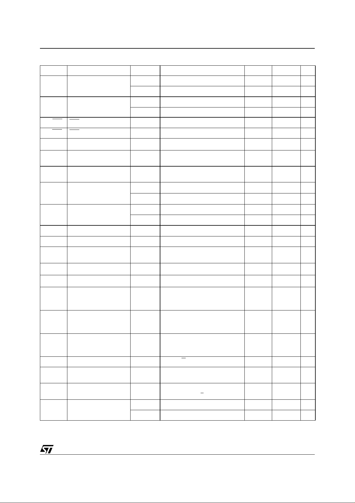
M50FW040
Table 18. DC Characteristics
Symbol Parameter Interface Test Condition Min Max Unit
V
V
V
V
(INIT)
IH
(INIT)
IL
I
LI
I
LI2
R
Input High Voltage
IH
Input Low Voltage
IL
Input High Voltage FWH 1.35
INIT
Input Low Voltage FWH –0.5
INIT
(2)
Input Leakage Current
IC, IDx Input Leakage
Current
IC, IDx Input Pull Low
IL
Resistor
FWH
A/A Mux
0.5 V
0.7 V
CCVCC
CCVCC
FWH –0.5
A/A Mux -0.5 0.8 V
0V ≤ V
IC, ID0, ID1, ID2, ID3 = V
IN
≤ V
CC
CC
20 100 kΩ
0.3 V
V
CC
0.2 V
+ 0.5
+ 0.3
CC
+ 0.5
CC
±10
200
V
V
V
V
V
µA
µA
V
V
V
OH
V
OL
I
LO
V
PP1
V
PPH
PPLK
LKO
I
CC1
Output High Voltage
Output Low Voltage
Output Leakage Current
VPP Volt age
VPP Volt age
(Fast Erase)
(1)
VPP Lockout Voltage
(1)
VCC Lockout Voltage
Supply Current (Standby) FWH
FWH I
A/A Mux
FWH
A/A Mux
FWH4 = 0.9 V
All other inputs 0.9 VCC to 0.1 V
= –500µA
OH
= –100µA
I
OH
I
= 1.5mA 0.1 V
OL
I
= 1.8mA
OL
0V ≤ V
OUT
CC
≤ V
CC
, VPP = V
VCC = 3.6V, f(CLK) = 33MHz
I
CC2
Supply Current (Standby) FWH
FWH4 = 0.1 V
All other inputs 0.9 VCC to 0.1 V
, VPP = V
CC
VCC = 3.6V, f(CLK) = 33MHz
= VCC max, VPP = V
I
CC3
(Any internal operation
FWH
active)
Supply Current
I
CC4
I
CC5
I
I
PP1
Note: 1. Sampled only, not 100% tested.
Supply Current (Read) A/A Mux
Supply Current
(1)
(Program/Erase)
VPP Supply Current
PP
(Read/Standby)
VPP Supply Current
(1)
A/A Mux Program/Erase Co ntr olle r Act ive 20 mA
(Program/Erase active)
2. Input leakage currents include High-Z output leakage for all bi-directional buffers with tri-state outputs.
V
CC
f(CLK) = 33MHz
I
G
= VIH, f = 6MHz
V
VPP = 12V ± 5%
OUT
V
PP
PP
= 0mA
> V
CC
= V
CC
CC
CC
CC
0.9 V
CC
V
– 0.4
CC
33.6V
11.4 12.6 V
1.5 V
1.8 2.3 V
CC
CC
CC
0.45 V
±10
µA
100 µA
10 mA
60 mA
20 mA
400 µA
40 mA
15 mA
V
V
V
25/41
Page 26
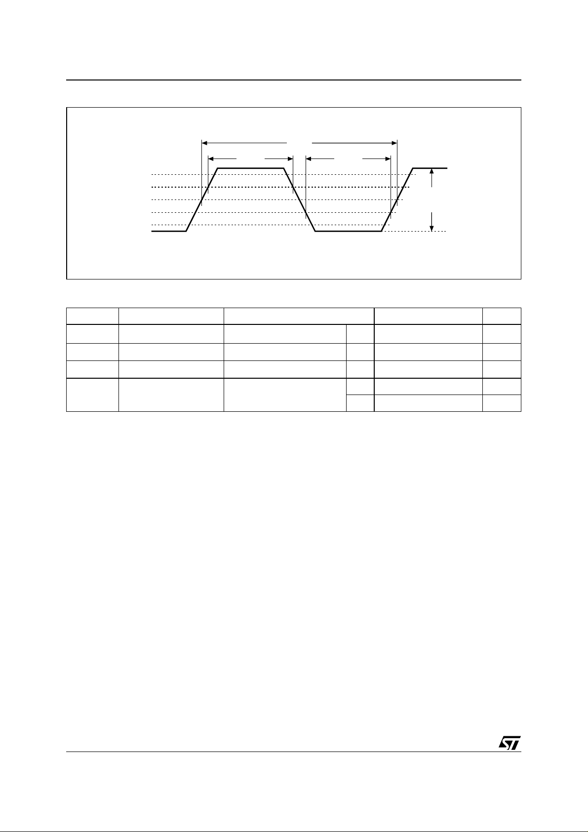
M50FW040
Figure 11. FWH Interface Clock Waveform
tCYC
tHIGH tLOW
0.6 V
CC
0.5 V
CC
0.4 V
CC
0.3 V
CC
0.2 V
CC
Table 19. FWH Interface Clock Characteristics
Symbol Parameter Test Condition Value Unit
t
CYC
t
HIGH
t
LOW
CLK Cycle Time
CLK High Time Min 11 ns
CLK Low Time Min 11 ns
CLK Slew Rate peak to peak
Note: 1. Devices on the PCI Bus must work with any clock frequency between DC and 33MHz. Below 16MHz devices may be guaranteed
by design rather than tested. Re fer to PCI Specification.
(1)
Min 30 ns
Min 1 V/ns
Max 4 V/ns
0.4 VCC,
(minimum)
p-to-p
AI03403
26/41
Page 27
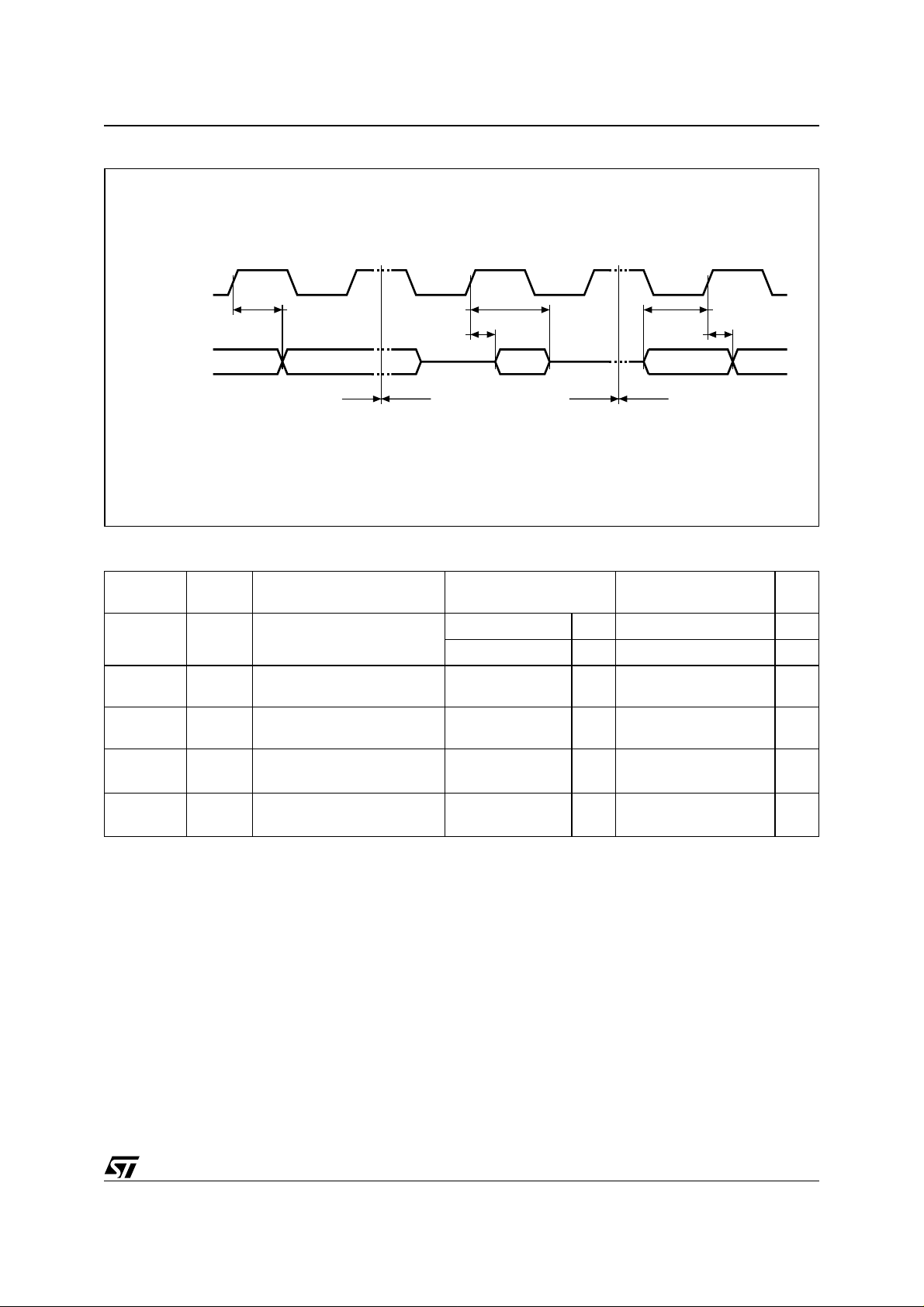
Figure 12. FWH Interface AC Signal Timing Waveforms
CLK
M50FW040
tCHQV
FWH0-FWH3
VALID OUTPUT DATA FLOAT OUTPUT DATA VALID INPUT DATA
tCHQZ
tCHQX
tDVCH
tCHDX
VALID
AI03405
Table 20. FWH Interface AC Signal Timing Characteristics
Symbol
t
CHQV
(1)
t
CHQX
t
CHQZ
t
AVCH
t
DVCH
t
CHAX
t
CHDX
Note: 1. The timing measurements for Active/Float transitions are defined when the curr ent thr ough the pin equals t he le akage c urrent spec-
ification.
2. Applies to all inputs except CLK.
PCI
Symbol
t
val
t
on
t
off
t
su
t
h
Parameter Test Condition Value Unit
CLK to Data Out
CLK to Active
(Float to Active Delay)
CLK to Inactive
(Active to Float Delay)
Input Set-up Time
Input Hold Time
(2)
(2)
Min 2 ns
Max 11 ns
Min 2 ns
Max 28 ns
Min 7 ns
Min 0 ns
27/41
Page 28
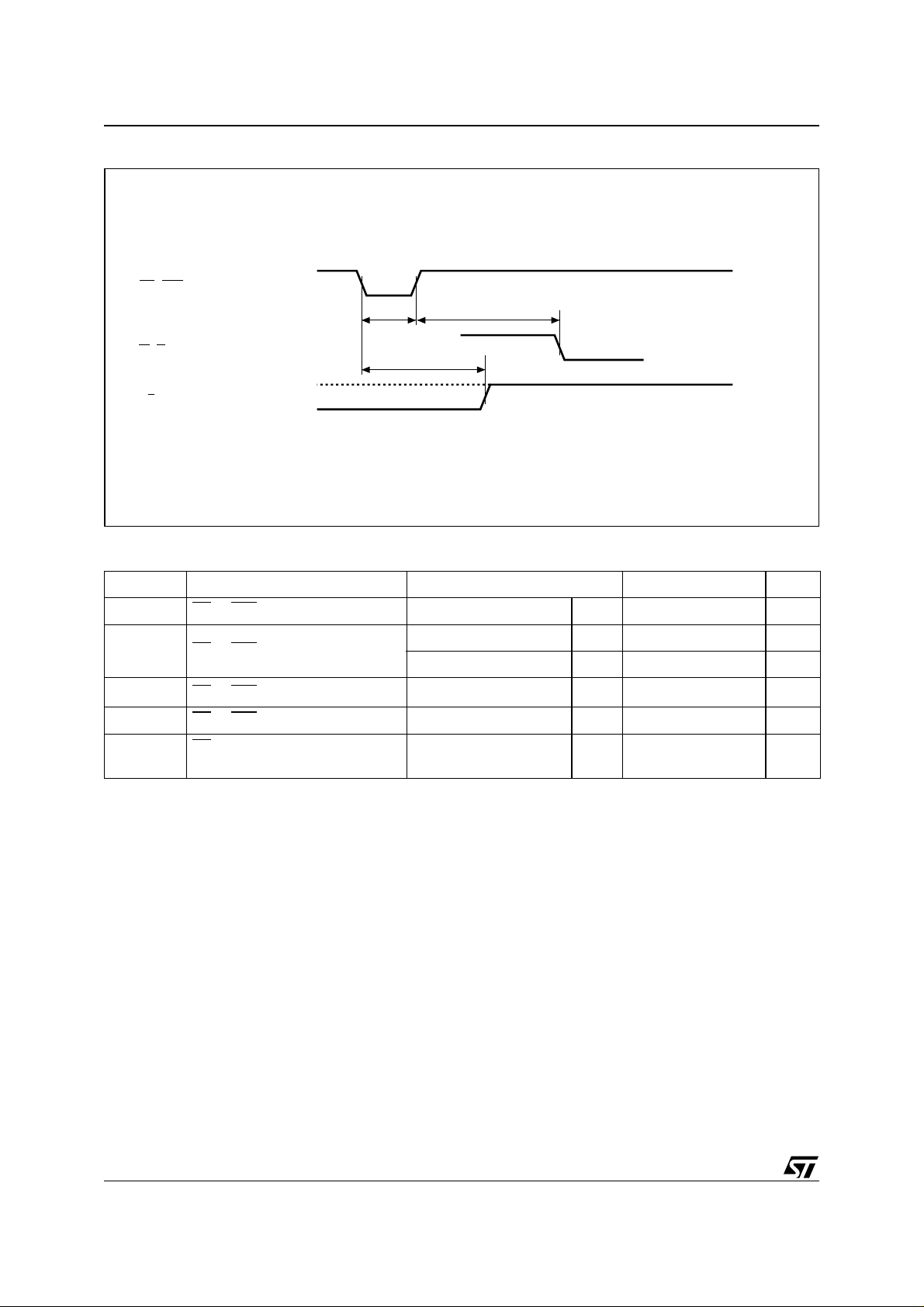
M50FW040
Figure 13. Reset AC Waveforms
RP, INIT
tPLPH
tPHWL, tPHGL, tPHFL
W, G, FWH4
RB
tPLRH
AI03420
Table 21. Reset AC Characteristics
Symbol Parameter Test Condition Value Unit
t
PLPH
t
PLRH
t
PHFL
t
PHWL
t
PHGL
Note: 1. See Chapter 4 of the PCI Specification.
RP or INIT Reset Pulse Width Min 100 ns
Program/Erase Inactive Max 100 ns
RP or INIT Low to Reset
Program/Erase Active Max 30 µs
RP
or INIT Slew Rate
(1)
Rising edge only Min 50 mV/ns
RP or INIT High to FWH4 Low FWH Interface only Min 30 µs
RP High to Writ e Enab le or Outp ut
Enable Low
A/A Mux Interface only Min 50 µs
28/41
Page 29
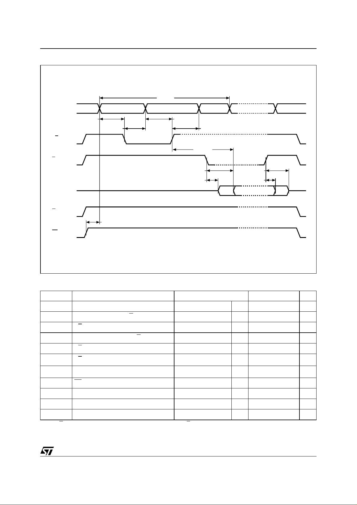
Figure 14. A/A Mux Interface Read AC Waveforms
tAVAV
M50FW040
A0-A10
RC
G
DQ0-DQ7
W
RP
ROW ADDR VALID NEXT ADDR VALID
tAVCL tAVCH
tCLAX tCHAX
tPHAV
COLUMN ADDR VALID
tCHQV
tGLQV
tGLQX
tGHQZ
tGHQX
VALID
AI03406
Table 22. A/A Mux Interface Read AC Characteristics
Symbol Parameter Test Condition Value Unit
t
AVAV
t
AVCL
t
CLAX
t
AVCH
t
CHAX
t
CHQV
t
GLQV
t
PHAV
t
GLQX
t
GHQZ
t
GHQX
Note: 1. G may be delayed up to t
Read Cycle Time Min 250 ns
Row Address Valid to RC Low Min 50 ns
RC Low to Row Address Transition Min 50 ns
Column Address Valid to RC high Min 50 ns
RC High to Column Address Transition Min 50 ns
(1)
RC High to Output Valid Max 150 ns
(1)
Output Enable Low to Output Valid Max 50 ns
RP High to Row Address Valid Min 1 µs
Output Enable Low to Output Transition Min 0 ns
Output Enable High to Output Hi-Z Max 50 ns
Output Hold from Output Enable High Min 0 ns
– t
CHQV
after the rising edge of RC withou t impac t on t
GLQV
CHQV
.
29/41
Page 30
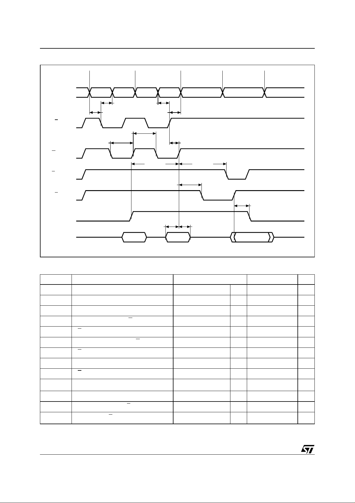
M50FW040
Figure 15. A/A Mux Interface Write AC Waveforms
A0-A10
RC
W
G
RB
V
PP
DQ0-DQ7
Write erase or
program setup
R1
tAVCL
tWLWH
C1
tCLAX
tWHWL
Write erase confirm or
valid address and data
R2 C2
tAVCH
tCHAX
tVPHWH tWHGL
D
IN1
tWHRL
Automated erase
or program delay
tCHWH
D
IN2
Read Status
Register Data
tQVVPL
tWHDXtDVWH
VALID SRD
Ready to write
another command
AI04185
Table 23. A/A Mux Interface Write AC Characteristics
Symbol Parameter Test Condition Value Unit
t
WLWH
t
DVWH
t
WHDX
t
AVCL
t
CLAX
t
AVCH
t
CHAX
t
WHWL
t
CHWH
t
VPHWH
t
WHGL
t
WHRL
t
QVVPL
Note: 1. Sampled only, not 100% tested.
2. A p pl i c a b l e i f V
Write Enable Low to Write Enable High Min 100 ns
Data Valid to Write Enable High Min 50 ns
Write Enable High to Data Transition Min 5 ns
Row Address Valid to RC Low Min 50 ns
RC Low to Row Address Transition Min 50 ns
Column Address Valid to RC High Min 50 ns
RC High to Column Address Transition Min 50 ns
Write Enable High to Write Enable Low Min 100 ns
RC High to Write Enable High Min 50 ns
(1)
VPP High to Write Enable High
Min 100 ns
Write Enable High to Output Enable Low Min 30 ns
Write Enable High to RB Low Min 0 ns
(1,2)
Output Valid, RB High to VPP Low
is seen as a logic input (VPP < 3.6V).
PP
Min 0 ns
30/41
Page 31
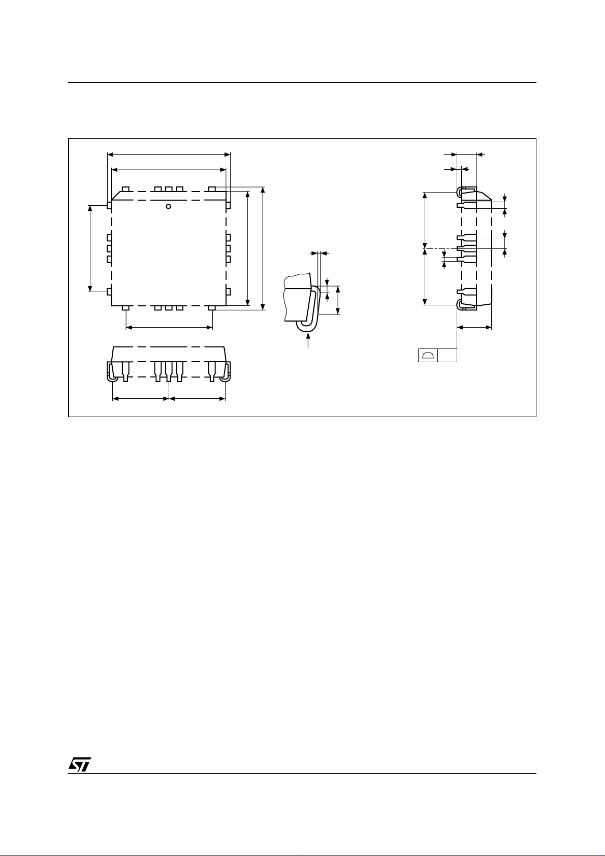
PACKAGE MECHANICAL
Figure 16. PLCC32 – 32 pin Rectangular Plastic Leaded Chip Carrier, Package Outline
M50FW040
E3
D2 D2
Note: Drawing is not to scale.
D
D1
1 N
D3
E1 E
R
F
0.51 (.020)
1.14 (.045)
A1
A2
B1
E2
e
B
E2
A
CP
PLCC-A
31/41
Page 32
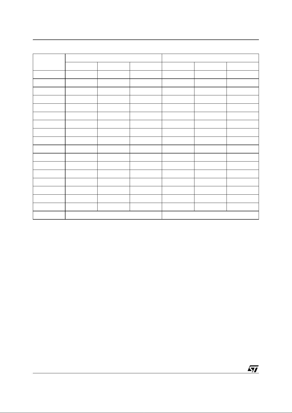
M50FW040
Table 24. PLCC32 – 32 pin Rectangular Plastic Leaded Chip Carrier, Package Mechanical Data
Symbol
Typ Min Max Typ Min Max
A 3.18 3.56 0.125 0.140
A1 1.53 2.41 0.060 0.095
A2 0.38 – 0.015 –
B 0.33 0.53 0.013 0.021
B1 0.66 0.81 0.026 0.032
CP 0.10 0.004
D 12.32 12.57 0.485 0.495
D1 11.35 11.51 0.447 0.453
D2 4.78 5.66 0.188 0.223
D3 7.62 – – 0.300 – –
E 14.86 15.11 0.585 0.595
E1 13.89 14.05 0.547 0.553
E2 6.05 6.93 0.238 0.273
E310.16– –0.400– –
e 1.27 – – 0.050 – –
F 0.00 0.13 0.000 0.005
R 0.89 – – 0.035 – –
N32 32
millimeters inches
32/41
Page 33
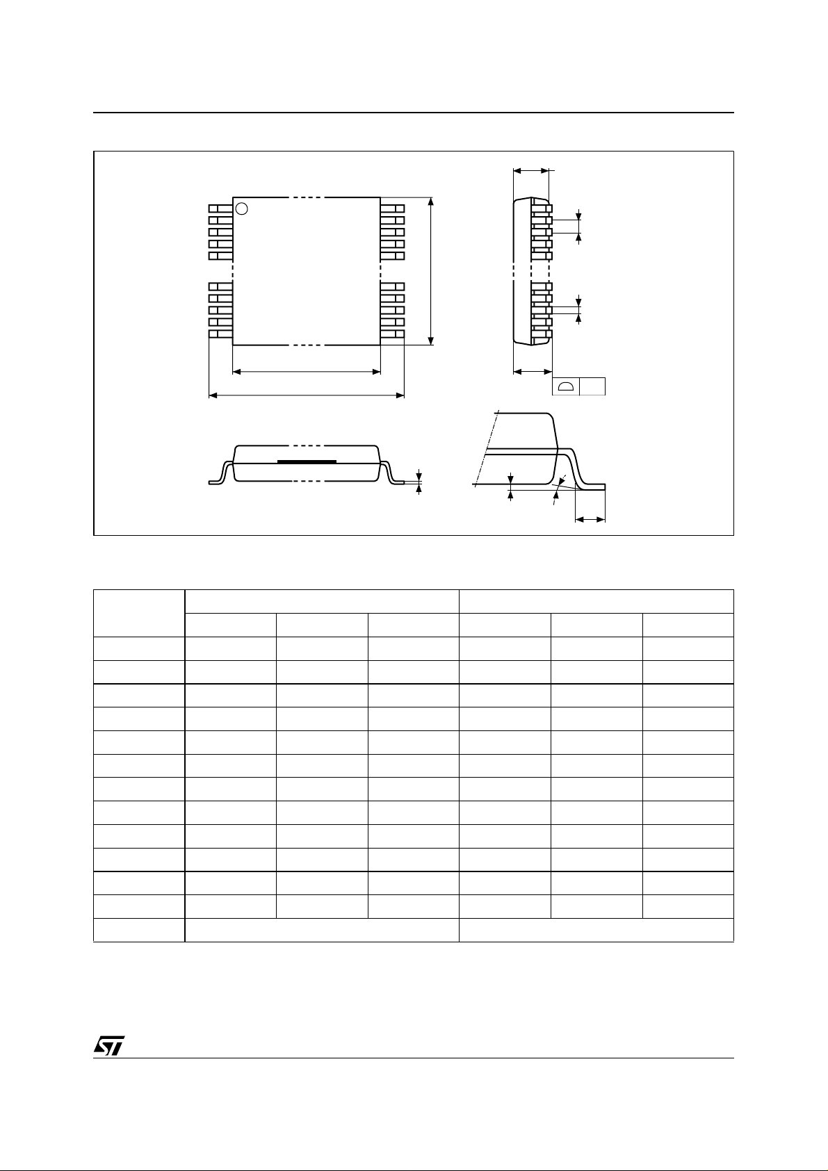
Figure 17. TSOP32 – 32 lead Plastic Thin Small Outline, 8x14 mm, Package Outline
A2
M50FW040
1
N
e
E
B
N/2
D1
D
DIE
A
CP
C
TSOP-a
Note: Drawing is not to scale.
LA1
α
Table 25. TSOP32 – 32 lead Plastic Thin Small Outline, 8x14 mm, Package Mechanical Data
Symbol
Typ Min Max Typ Min Max
A 1.200 0.0472
A1 0.050 0.150 0.0020 0.0059
A2 0.950 1.050 0.0374 0.0413
α 0° 5° 0° 5°
B 0.170 0.270 0.0067 0.0106
C 0.100 0.210 0.0039 0.0083
CP 0.100 0.0039
D 13.800 14.200 0.5433 0.5591
D1 12.300 12.500 0.4843 0.4921
e 0.500 – – 0.0197 – –
E 7.900 8.100 0.3110 0.3189
L 0.500 0.700 0.0197 0.0276
N32 32
millimeters inches
33/41
Page 34
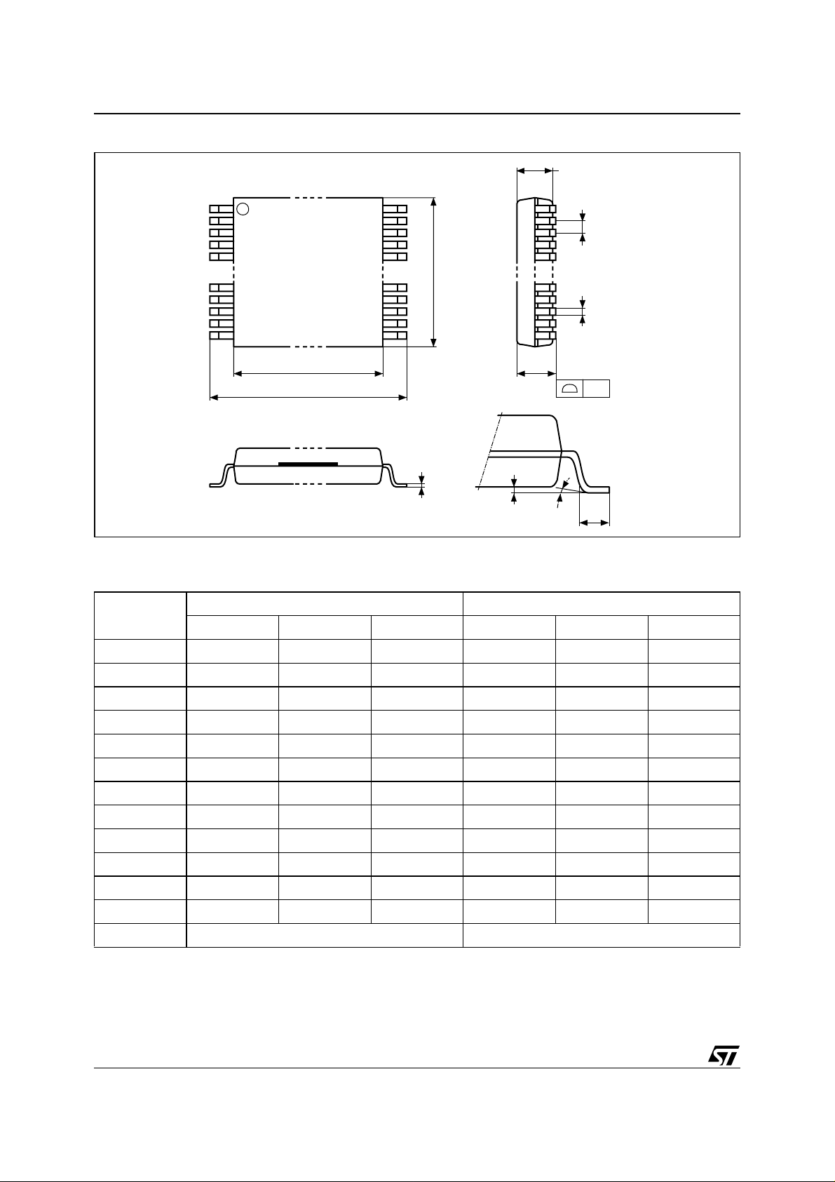
M50FW040
Figure 18. TSOP40 – 40 lead Plastic Thin Small Outline, 10x20 mm, Package Outline
A2
1
N
e
E
B
N/2
D1
D
DIE
A
CP
C
TSOP-a
Note: Drawing is not to scale.
LA1
α
Table 26. TSOP40 – 40 lead Plastic Thin Small Outline, 10x20 mm, Package Mechanical Data
Symbol
Typ Min Max Typ Min Max
A 1.200 0.0472
A1 0.050 0.150 0.0020 0.0059
A2 0.950 1.050 0.0374 0.0413
B 0.170 0.270 0.0067 0.0106
C 0.100 0.210 0.0039 0.0083
CP 0.100 0.0039
D 19.800 20.200 0.7795 0.7953
D1 18.300 18.500 0.7205 0.7283
e 0.500 – – 0.0197 – –
E 9.900 10.100 0.3898 0.3976
L 0.500 0.700 0.0197 0.0276
α 0° 5° 0° 5°
N40 40
millimeters inches
34/41
Page 35

PART NUMBERING
Table 27. Ordering Information Scheme
Example: M50FW040 K1TG
Device Type
M50
Architecture
F = Firmware Hub Interface
Operating Voltage
W = 3V to 3.6V
Device Function
040 = 4 Mbit (x8), Uniform Block
Package
K = PLCC32
NB = TSOP32 (8 x 14mm)
N = TSOP40: 10 x 20 mm
M50FW040
Device Grade
5 = Temperature range –20 to 85 °C.
Device tested with standard test flow
1 = Temperature range 0 to 70 °C.
Device tested with standard test flow
Option
blank = Standard Packing
T = Tape & Reel Packing
Plating Technology
blank = Standard SnPb plating
G = Lead-Free, RoHS compliant, Sb2O3-free and TBBA-free
Devices are shipped from the factory with the memory content bits erased to ’1’.
For a list of available options (Speed, Package, etc.) or for further information on any aspect of this device,
please contact the ST Sales Office nearest to you.
35/41
Page 36
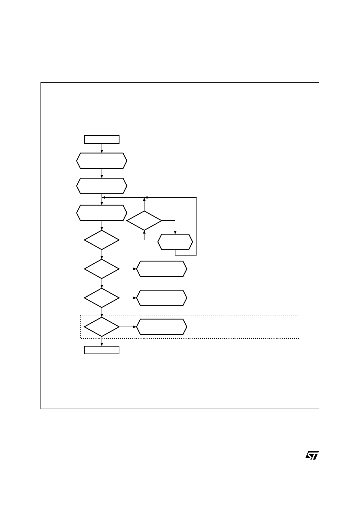
M50FW040
FLOWCHARTS AND PSEUDO CODES
Figure 19. Program Flowchart and Pseudo Code
Start
FWH
Interface
Only
Write 40h or 10h
Write Address
& Data
Read Status
Register
b7 = 1
YES
b3 = 0
YES
b4 = 0
YES
b1 = 0
YES
End
NO
NO
NO
NO
NO
Suspend
Program to Protected
Block Error (1, 2)
YES
Suspend
VPP Invalid
Error (1, 2)
Program
Error (1, 2)
Program command:
– write 40h or 10h
– write Address & Data
(memory enters read status state after
the Program command)
do:
–read Status Register if Program/Erase
Suspend command given execute
suspend program loop
Loop
while b7 = 1
If b3 = 1, VPP invalid error:
– error handler
If b4 = 1, Program error:
– error handler
If b1 = 1, Program to protected block error:
– error handler
AI03407
Note: 1. A Status check of b1 (Protected Block), b3 (VPP invalid) and b4 (Program Error) can be made after each Program operation by
following the correct command sequence.
2. If an error is found, the Status Register must be cleared before further Program/Erase Controller operations.
36/41
Page 37
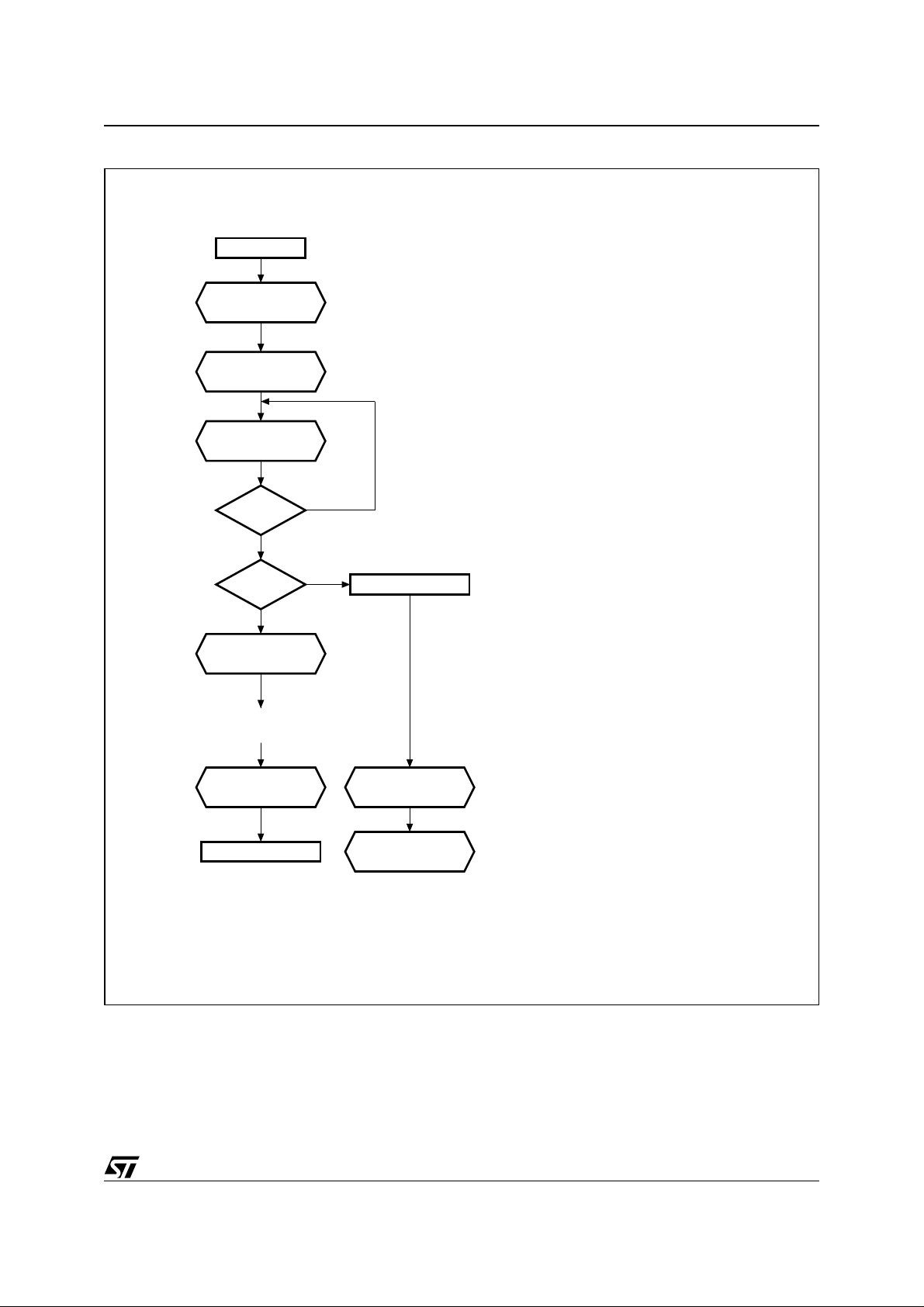
Figure 20. Program Suspend & Resume Flowchart and Pseudo Code
Start
Write B0h
Program/Erase Suspend command:
Write 70h
Read Status
Register
– write B0h
– write 70h
do:
– read Status Register
M50FW040
b7 = 1
YES
b2 = 1
YES
Write a read
Command
Read data from
another address
Write D0h
Program Continues
NO
NO
Program Complete
Write FFh
Read Data
while b7 = 1
If b2 = 0 Program completed
Program/Erase Resume command:
– write D0h to resume the program
– if the Program operation completed
then this is not necessary.
The device returns to Read as
normal (as if the Program/Erase
suspend was not issued).
AI03408
37/41
Page 38
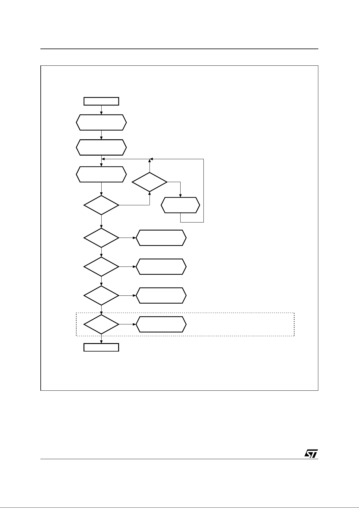
M50FW040
Figure 21. Erase Flowchart and Pseudo Code
Start
Write 20h
Write Block Address
& D0h
Read Status
Register
b7 = 1
YES
b3 = 0
YES
b4, b5 = 0
YES
b5 = 0
NO
NO
NO
NO
NO
Suspend
VPP Invalid
Sequence Error (1)
Erase Error (1)
YES
Suspend
Error (1)
Command
Erase command:
– write 20h
– write Block Address & D0h
(memory enters read Status Register after
the Erase command)
do:
– read Status Register
– if Program/Erase Suspend command
given execute suspend erase loop
Loop
while b7 = 1
If b3 = 1, VPP invalid error:
– error handler
If b4, b5 = 1, Command sequence error:
– error handler
If b5 = 1, Erase error:
– error handler
YES
FWH
Interface
Only
Note: 1. If an error is found, the Status Register must be cleared before further Program/E rase Controller operations.
b1 = 0
End
YES
NO
Erase to Protected
Block Error (1)
If b1 = 1, Erase to protected block error:
– error handler
38/41
AI03409
Page 39
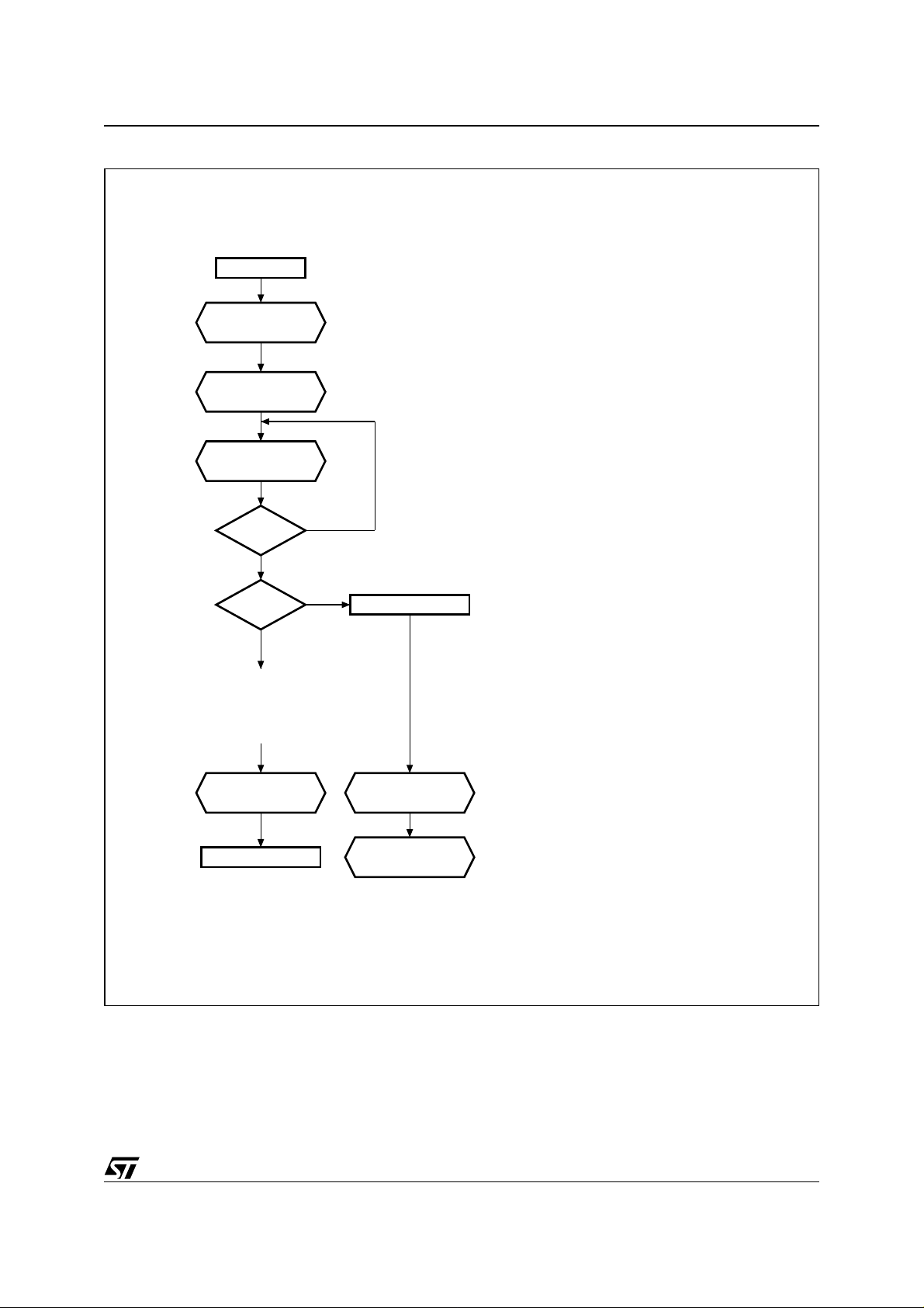
Figure 22. Erase Suspend & Resume Flowchart and Pseudo Code
Start
Write B0h
Program/Erase Suspend command:
Write 70h
– write B0h
– write 70h
M50FW040
Read Status
Register
b7 = 1
YES
b6 = 1
YES
Read data from
another block
or
Program
Write D0h
Erase Continues
NO
NO
Erase Complete
Write FFh
Read Data
do:
– read Status Register
while b7 = 1
If b6 = 0, Erase completed
Program/Erase Resume command:
– write D0h to resume erase
– if the Erase operation completed
then this is not necessary.
The device returns to Read as
normal (as if the Program/Erase
suspend was not issued).
AI03410
39/41
Page 40
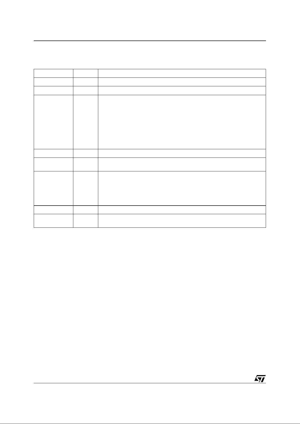
M50FW040
REVISION HISTORY
Table 28. Document Revision History
Date Version Revision Details
September 2000 - 01 First Issue
04-Oct-2000 -02
11-Apr-01 -03 Document type: from Preliminary Data to Data Sheet
06-Jul-2001 -04 Note 2 changed (Table 13., Abs olu te Maxim u m Ra ting s)
12-Mar-2002 -05
09-Jul-2004 6.0
12-Jul-2004 7.0 Inches values corrected in Table 27., Ordering Information Scheme.
10-Nov-2004 8.0
DC Characteristics: I
Program and Erase functions clarification
Read Electronic Signature table change
FWH Register Configuration Map table change
Input Register Definition table, note clarification
DC Characteristics parameters clarification and new V
FWH Interface AC Signal Timing Characteristics change
A/A Mux Interface Read AC Characteristics change
A/A Mux Interface Write AC Characteristics change
A/A Mux Interface Write AC Waveforms change
RFU pins must be left disconnected
Specification of PLCC32 package mechanical data revised
Revision numbering modified.
Document imported in new template (and so reformatted).
Temperature Range ordering information replaced by Device Grade, Standard
packing option added and Plating Technology added to Table 27., Ordering
Information Scheme. T
Ratings and T
TSOP32 package added. Figure 3., Logic Diagram (A/A Mux Interface) and Table
2., Signal Names (A/A Mux Interface) added.
BIAS
changed
CC4
parameter added to Table 13., Absolute Maximum
LEAD
parameter removed.
and VIL parameters added
IH
40/41
Page 41

M50FW040
Information furnished is be lieved to be a ccur ate and reli able. Howe ver, STMicroele ctronic s assu mes no r esponsib ilit y for th e consequences
of use of such information nor for any infrin gement of patent s or other rights of third parties which ma y result from it s use. No license is granted
by implication or otherwi se under any patent or patent rights of STMicroelectronic s. Specifications mentioned in this publication a re subject
to change without not ice. This pub licat ion su persed es and repl aces all in format ion previou sly su pplie d. STMicroele c tronic s prod ucts ar e no t
authorized for use as critical compone nts in life support devices or systems without express written approval of STMicroelectronics.
The ST logo is a registered trademark of STMicroelectronics.
All other names are the property of their respective owners
© 2004 STMicroelectronics - All rights reserved
Australia - Belgium - Brazil - Canada - China - Czech Republic - Finland - France - Germany - Hong Kong - India - Israel - Italy - Japan -
Malaysia - Malta - Morocco - Singapore - Spain - Sweden - Switzerland - United Kingdom - United States of America
STMicroelectronics group of companies
www.st.com
41/41
 Loading...