

Page 1
SEMICONDUCTOR TECHNICAL DATA
The M4N37 device consists of a gallium arsenide infrared emitting diode
optically coupled to a monolithic silicon phototransistor detector.
• Current Transfer Ratio — 100% Minimum @ Specified Conditions
• Guaranteed Switching Speeds
• Meets or Exceeds All JEDEC Registered Specifications
Applications
• General Purpose Switching Circuits
• Interfacing and coupling systems of different potentials and impedances
• Regulation Feedback Circuits
• Monitor & Detection Circuits
• Solid State Relays
Order this document
by M4N37/D
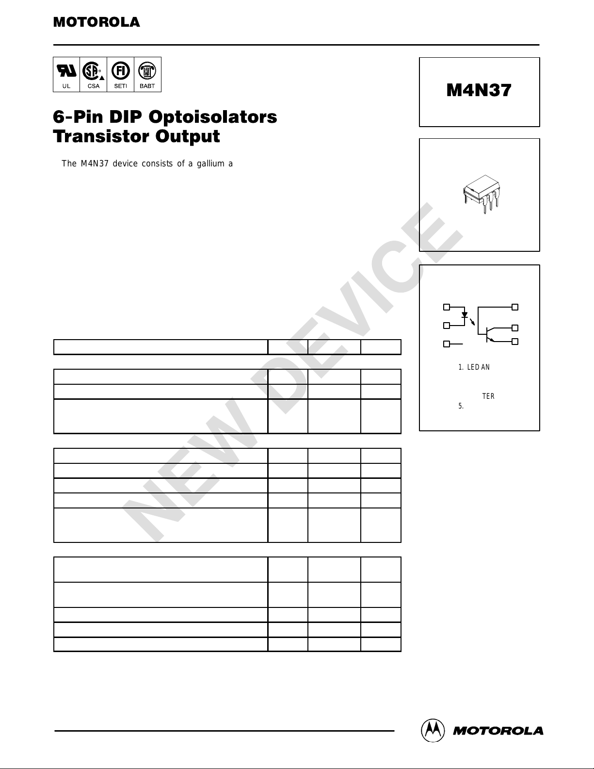
STYLE 1 PLASTIC
6
1
STANDARD THRU HOLE
SCHEMATIC
1
6
MAXIMUM RATINGS
INPUT LED
Reverse Voltage V
Forward Current — Continuous I
LED Power Dissipation @ TA = 25°C
with Negligible Power in Output Detector
Derate above 25°C
OUTPUT TRANSISTOR
Collector–Emitter Voltage V
Emitter–Base Voltage V
Collector–Base Voltage V
Collector Current — Continuous I
Detector Power Dissipation @ TA = 25°C
with Negligible Power in Input LED
Derate above 25°C
TOTAL DEVICE
Isolation Source Voltage
(Peak ac Voltage, 60 Hz, 1 sec Duration)
Total Device Power Dissipation @ TA = 25°C
Derate above 25°C
Ambient Operating Temperature Range
Storage Temperature Range
Soldering Temperature (10 sec, 1/16″ from case) T
1. Isolation surge voltage is an internal device dielectric breakdown rating.
1. For this test, Pins 1 and 2 are common, and Pins 4, 5 and 6 are common.
2. Refer to Quality and Reliability Section in Opto Data Book for information on test conditions.
(TA = 25°C unless otherwise noted)
Rating
(1)
(2)
(2)
Symbol Value Unit
6 Volts
60 mA
100
1.41
30 Volts
7 Volts
70 Volts
50 mA
150
1.76
7500 Vac(pk)
250
2.94
–55 to +100 °C
–55 to +150 °C
260 °C
mW/°C
mW/°C
mW/°C
P
CEO
EBO
CBO
P
V
ISO
P
T
T
R
F
D
C
D
D
A
stg
L
mW
mW
mW
2
3
PIN 1. LED ANODE
2. LED CATHODE
3. N.C.
4. EMITTER
5. COLLECTOR
6. BASE
5
4
Motorola Optoelectronics Device Data
Motorola, Inc. 1997
1
Page 2
M4N37
(
C
,
CC
,
ELECTRICAL CHARACTERISTICS
Characteristic
INPUT LED
Forward Voltage (IF = 10 mA) TA = 25°C
Reverse Leakage Current (VR = 6 V) I
Capacitance (V = 0 V, f = 1 MHz) C
OUTPUT TRANSISTOR
Collector–Emitter Dark Current (VCE = 10 V, TA = 25°C)
Collector–Base Dark Current (VCB = 10 V) TA = 25°C
Collector–Emitter Breakdown Voltage (IC = 1 mA) V
Collector–Base Breakdown Voltage (IC = 100 µA) V
Emitter–Base Breakdown Voltage (IE = 100 µA) V
DC Current Gain (IC = 2 mA, VCE = 5 V) h
Collector–Emitter Capacitance (f = 1 MHz, VCE = 0) C
Collector–Base Capacitance (f = 1 MHz, VCB = 0) C
Emitter–Base Capacitance (f = 1 MHz, VEB = 0) C
COUPLED
Output Collector Current TA = 25°C
(IF = 10 mA, VCE = 10 V) TA = –55°C
Collector–Emitter Saturation Voltage (IC = 0.5 mA, IF = 10 mA) V
Turn–On Time
Turn–Off Time
Rise Time
Fall Time t
Isolation Voltage (f = 60 Hz, t = 1 sec) V
Isolation Current
Isolation Resistance (V = 500 V)
Isolation Capacitance (V = 0 V , f = 1 MHz)
1. Always design to the specified minimum/maximum electrical limits (where applicable).
2. Current Transfer Ratio (CTR) = IC/IF x 100%.
3. For test circuit setup and waveforms, refer to Figure 14.
4. For this test, Pins 1 and 2 are common, and Pins 4, 5 and 6 are common.
(4)
(V
= 1500 Vpk) I
I–O
(TA = 25°C unless otherwise noted)
TA = –55°C
TA = 100°C
(VCE = 30 V, TA = 100°C)
TA = 100°C
TA = 100°C
(IC = 2 mA, VCC = 10 V,
RL = 100 Ω)
(4)
(4)
(3)
(1)
Symbol Min Typ
V
R
I
CEO
I
CBO
(BR)CEO
(BR)CBO
(BR)EBO
FE
CE
CB
EB
IC (CTR)
CE(sat)
t
on
t
off
t
ISO
ISO
R
ISO
C
ISO
F 0.8
J
(2)
r
f
0.9
0.7
— — 10 µA
— 18 — pF
—
—
— 0.2
30 45 — Volts
70 100 — Volts
— 400 — —
— 7 — pF
— 19 — pF
— 9 — pF
10 (100)
4 (40)
4 (40)
— 0.14 0.3 Volts
— 7.5 10
— 5.7 10
— 3.2 —
— 4.7 —
7500 — — Vac(pk)
— 8 100 µA
10
— 0.2 2 pF
(1)
1.15
1.3
1.05
1
—
100
7 7.8 — Volts
30 (300)
—
—
11
— — Ω
Max Unit
1.5
1.7
1.4
50
500
20
—
—
—
—
Volts
nA
µA
nA
mA (%)
µs
2
Motorola Optoelectronics Device Data
Page 3
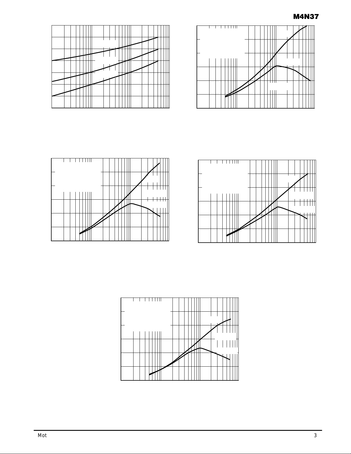
1.4
1.3
1.2
1.1
TA = –55°C
TA = 25°C
1.5
NORMALIZED TO:
VCE = 10 V
IF = 10 mA
TA = 25
1.0
CTR
°
C
CE(sat) VCE
= 0.4 V
NCTR
NCTR
M4N37
(sat)
, FORWARD VOLTAGE (V)
F
V
1.0
0.9
0.8
0.7
TA = 85°C
0.5
NCTR, NORMALIZED CTR
1.0 1.0
IF, FORWARD CURRENT (mA)
10 1000.1
0
TA = 25°C
10 1000
IF, LED CURRENT (mA)
Figure 1. Forward Voltage vs. Forward Current Figure 2. Normalized Non–Saturated and
Saturated CTR, TA = 25°C vs. LED Current
1.5
NORMALIZED TO:
VCE = 10 V
IF = 10 mA
TA = 25
°
CTR
CE(sat) VCE
C
= 0.4 V
1.0
0.5
NCTR, NORMALIZED CTR
NCTR
TA = 50°C
NCTR
(sat)
1.5
NORMALIZED TO:
VCE = 10 V
IF = 10 mA
TA = 25
°
CTR
CE(sat) VCE
C
= 0.4 V
1.0
0.5
NCTR, NORMALIZED CTR
NCTR
TA = 70°C
NCTR
(sat)
0
1.0
IF, LED CURRENT (mA)
10 1000.1
Figure 3. Normalized Non–Saturated and Saturated
CTR, TA = 50°C vs. LED Current
1.5
NORMALIZED TO:
VCE = 10 V
IF = 10 mA
TA = 25
°
CTR
CE(sat) VCE
C
= 0.4 V
1.0
IF, LED CURRENT (mA)
1.0
0.5
NCTR, NORMALIZED CTR
0
0
1.0
IF, LED CURRENT (mA)
10 1000.1
Figure 4. Normalized Non–Saturated and Saturated
CTR, TA = 70°C vs. LED Current
NCTR
TA = 85°C
NCTR
(sat)
10 1000.1
Figure 5. Normalized Non–Saturated and Saturated
Motorola Optoelectronics Device Data
CTR, TA = 85°C vs. LED Current
3
Page 4

M4N37
5
35
30
25
20
15
10
, COLLECTOR CURRENT (mA)
CE
I
5.0
0
10
25°C
50°C
85°C
70°C
100
20
IF, LED CURRENT (mA)
30 40 50 60
, COLLECTOR–EMITTER (nA)I
CEO
10
10
10
10
10
10
10
–1
–2
4
3
2
1
0
040–20
20
TA, AMBIENT TEMPERATURE (
TYPICAL
VCE = 10 V
60 10080
°
C)
Figure 6. Collector–Emitter Current
vs. Temperature and LED Current
1.5
NORMALIZED TO:
IF = 10 mA
VCB = 9.3 V
TA = 25
°
1.0
, NORMALIZED CTR
0.5
CB CB
NCTR
0
C
25°C
50°C
70°C
Figure 8. Normalized CTRcb vs. LED
1.0
IF, LED CURRENT (mA)
10 1000.1
Current and Temperature
10
NORMALIZED TO:
IF = 10 mA
TA = 25
1.0
0.1
NORMALIZED PHOTOCURRENT
0.01
Figure 7. Collector–Emitter Leakage
Current vs. Temperature
–20°C
°
C
1.0
IF, LED CURRENT (mA)
25°C
50°C
10 1000.1
Figure 9. Normalized Photocurrent vs.
lF and T emperature
70°C
1.2
70°C
50°C
1.0
25°C
–20°C
0.8
, NORMALIZED H
FE FE
0.6
NH
0.4
10
IB, BASE CURRENT (mA)
NORMALIZED TO:
VCE = 10 V
IB = 20
m
TA = 25
°
C
100 10001.0
A
Figure 10. Normalized Non–Saturated HFE vs. Base
Current and Temperature
4
Motorola Optoelectronics Device Data
Page 5

1.5
1.0
0.5
, NORMALIZED SATURATED H
FE(sat) FE
NH
0
70°C
25°C
–20°C
VCE = 0.4 V
50°C
10
IB, BASE CURRENT (
NORMALIZED TO:
VCE = 10 V
IB = 20
TA = 25
100 10001.0
m
A)
M4N37
1000
m
A
°
C
m
100
10
, PROPAGATION DELAY ( s)
LH
tp
1.0
tp
HL
tp
LH
RL, COLLECTOR LOAD RESISTOR (KW)
TA = 25°C
IF = 10 mA
VCC = 5.0 V
VTH = 1.5 V
1.00.1
10 100
2.5
2.0
1.5
1.0
m
, PROPAGATION DELAY ( s)
HL
tp
Figure 1 1. Normalized HFE vs. Base Current
and Temperature
I
F
V
O
Figure 13. Switching Timing
Figure 12. Propagation Delay vs. Collector
Load Resistor
t
D
t
R
t
PLH
VTH = 1.5 V
t
PHL
t
S
t
F
Motorola Optoelectronics Device Data
VCC = 5.0 V
F = 10 KHz
DF = 50%
IF = 10 mA
R
L
Figure 14. Switching Schematic
V
O
5
Page 6

M4N37
Package Dimensions in Inches (mm)
0.248 (6.30)
0.256 (6.50)
_
4 typ.
0.018 (0.45)
0.022 (0.55)
1
23
46
5
PIN ONE
ID.
0.335 (8.50)
0.343 (8.70)
0.039 (1.00)
min.
0.130 (3.30)
0.138 (3.50)
0.031 (0.80)
min.
0.031 (0.80)
0.035 (0.90)
0.100 (2.54) typ.
ANODE
CATHODE
NC
0.010 (0.25)
typ.
3
0.300 (7.62)
typ.
18 typ.
_
0.300 (7.62)
0.347 (8.82)
BASE
61
COLLECTOR
52
EMITTER
4
0.114 (2.90)
0.130 (3.30)
6
Motorola Optoelectronics Device Data
Page 7

M4N37
Motorola reserves the right to make changes without further notice to any products herein. Motorola makes no warranty , representation or guarantee regarding
the suitability of its products for any particular purpose, nor does Motorola assume any liability arising out of the application or use of any product or circuit, and
specifically disclaims any and all liability, including without limitation consequential or incidental damages. “T ypical” parameters which may be provided in Motorola
data sheets and/or specifications can and do vary in different applications and actual performance may vary over time. All operating parameters, including “Typicals”
must be validated for each customer application by customer’s technical experts. Motorola does not convey any license under its patent rights nor the rights of
others. Motorola products are not designed, intended, or authorized for use as components in systems intended for surgical implant into the body, or other
applications intended to support or sustain life, or for any other application in which the failure of the Motorola product could create a situation where personal injury
or death may occur. Should Buyer purchase or use Motorola products for any such unintended or unauthorized application, Buyer shall indemnify and hold Motorola
and its officers, employees, subsidiaries, affiliates, and distributors harmless against all claims, costs, damages, and expenses, and reasonable attorney fees
arising out of, directly or indirectly, any claim of personal injury or death associated with such unintended or unauthorized use, even if such claim alleges that
Motorola was negligent regarding the design or manufacture of the part. Motorola and are registered trademarks of Motorola, Inc. Motorola, Inc. is an Equal
Opportunity/Affirmative Action Employer.
Motorola Optoelectronics Device Data
7
Page 8

M4N37
How to reach us:
USA/EUROPE/Locations Not Listed: Motorola Literature Distribution; JAPAN: Nippon Motorola Ltd.; Tatsumi–SPD–JLDC, 6F Seibu–Butsuryu–Center,
P.O. Box 5405, Denver, Colorado 80217. 303–675–2140 or 1–800–441–2447 3–14–2 T atsumi Koto–Ku, Tokyo 135, Japan. 81–3–3521–8315
Mfax: RMFAX0@email.sps.mot.com – TOUCHTONE 602–244–6609 ASIA/PACIFIC: Motorola Semiconductors H.K. Ltd.; 8B Tai Ping Industrial Park,
INTERNET: http://www.mot.com/SPS/
8
– US & Canada ONLY 1–800–774–1848 51 Ting Kok Road, T ai Po, N.T., Hong Kong. 852–26629298
◊
Mfax is a trademark of Motorola, Inc.
Motorola Optoelectronics Device Data
M4N37/D
 Loading...