

Page 1
M48Z58
M48Z58Y
5 V, 64 Kbit (8 Kbit x 8) ZEROPOWER® SRAM
Features
■ Integrated, ultra low power SRAM, power-fail
control circuit, and battery
■ READ cycle time equals WRITE cycle time
■ Automatic power-fail chip deselect and WRITE
protection
■ WRITE protect voltages:
(V
= power-fail deselect voltage)
PFD
–M48Z58: V
4.5 V ≤ V
–M48Z58Y: V
4.2 V ≤ V
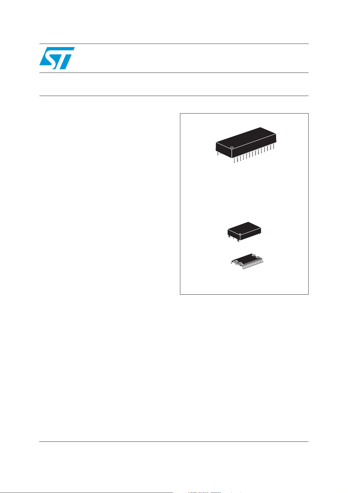
■ Self-contained battery in the CAPHAT
package
■ Packaging includes a 28-lead SOIC and
SNAPHAT
■ SOIC package provides direct connection for a
SNAPHAT
■ Pin and function compatible with JEDEC
standard 8 Kbit x 8 SRAMs
■ RoHS compliant
– Lead-free second level interconnect
= 4.75 to 5.5 V;
CC
≤ 4.75 V
PFD
= 4.5 to 5.5 V;
CC
≤ 4.5 V
PFD
®
top (to be ordered separately)
®
top which contains the battery
™
DIP
28
1
PCDIP28
battery CAPHAT™
®
battery
1
SOH28
2
8
SNAPHAT
June 2011 Doc ID 2559 Rev 11 1/24
www.st.com
1
Page 2

Contents M48Z58, M48Z58Y
Contents
1 Description . . . . . . . . . . . . . . . . . . . . . . . . . . . . . . . . . . . . . . . . . . . . . . . . . 5
2 Operating modes . . . . . . . . . . . . . . . . . . . . . . . . . . . . . . . . . . . . . . . . . . . . 8
2.1 READ mode . . . . . . . . . . . . . . . . . . . . . . . . . . . . . . . . . . . . . . . . . . . . . . . . 8
2.2 WRITE mode . . . . . . . . . . . . . . . . . . . . . . . . . . . . . . . . . . . . . . . . . . . . . . . 9
2.3 Data retention mode . . . . . . . . . . . . . . . . . . . . . . . . . . . . . . . . . . . . . . . . . 11
2.4 V
noise and negative going transients . . . . . . . . . . . . . . . . . . . . . . . . . 12
CC
3 Maximum ratings . . . . . . . . . . . . . . . . . . . . . . . . . . . . . . . . . . . . . . . . . . . 13
4 DC and AC parameters . . . . . . . . . . . . . . . . . . . . . . . . . . . . . . . . . . . . . . 14
5 Package mechanical data . . . . . . . . . . . . . . . . . . . . . . . . . . . . . . . . . . . . 17
6 Part numbering . . . . . . . . . . . . . . . . . . . . . . . . . . . . . . . . . . . . . . . . . . . . 21
7 Environmental information . . . . . . . . . . . . . . . . . . . . . . . . . . . . . . . . . . . 22
8 Revision history . . . . . . . . . . . . . . . . . . . . . . . . . . . . . . . . . . . . . . . . . . . 23
2/24 Doc ID 2559 Rev 11
Page 3

M48Z58, M48Z58Y List of tables
List of tables
Table 1. Signal names . . . . . . . . . . . . . . . . . . . . . . . . . . . . . . . . . . . . . . . . . . . . . . . . . . . . . . . . . . . . 6
Table 2. Operating modes . . . . . . . . . . . . . . . . . . . . . . . . . . . . . . . . . . . . . . . . . . . . . . . . . . . . . . . . . 8
Table 3. READ mode AC characteristics . . . . . . . . . . . . . . . . . . . . . . . . . . . . . . . . . . . . . . . . . . . . . . 9
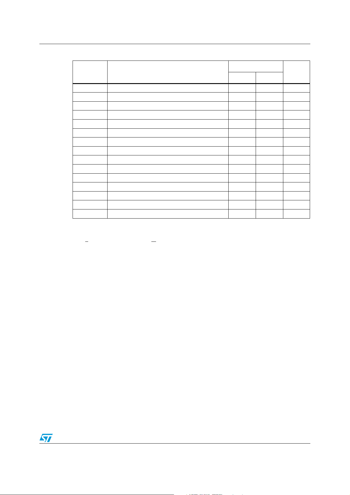
Table 4. WRITE mode AC characteristics . . . . . . . . . . . . . . . . . . . . . . . . . . . . . . . . . . . . . . . . . . . . 11
Table 5. Absolute maximum ratings . . . . . . . . . . . . . . . . . . . . . . . . . . . . . . . . . . . . . . . . . . . . . . . . . 13
Table 6. Operating and AC measurement conditions . . . . . . . . . . . . . . . . . . . . . . . . . . . . . . . . . . . . 14
Table 7. Capacitance . . . . . . . . . . . . . . . . . . . . . . . . . . . . . . . . . . . . . . . . . . . . . . . . . . . . . . . . . . . . 14
Table 8. DC characteristics. . . . . . . . . . . . . . . . . . . . . . . . . . . . . . . . . . . . . . . . . . . . . . . . . . . . . . . . 15
Table 9. Power down/up AC characteristics . . . . . . . . . . . . . . . . . . . . . . . . . . . . . . . . . . . . . . . . . . . 16
Table 10. Power down/up trip points DC characteristics . . . . . . . . . . . . . . . . . . . . . . . . . . . . . . . . . . 16
Table 11. PCDIP28 – 28-pin plastic DIP, battery CAPHAT™, pack. mech. data . . . . . . . . . . . . . . . . 17
Table 12. SOH28 – 28-lead plastic small outline, battery SNAPHAT
Table 13. SH – 4-pin SNAPHAT
Table 14. SH – 4-pin SNAPHAT
Table 15. Ordering information scheme . . . . . . . . . . . . . . . . . . . . . . . . . . . . . . . . . . . . . . . . . . . . . . . 21
Table 16. SNAPHAT
®
battery table . . . . . . . . . . . . . . . . . . . . . . . . . . . . . . . . . . . . . . . . . . . . . . . . . . 21
®
housing for 48 mAh battery, package mech. data . . . . . . . . . . . . 19
®
housing for 120 mAh battery, pack. mech. data . . . . . . . . . . . . . . 20
Table 17. Document revision history . . . . . . . . . . . . . . . . . . . . . . . . . . . . . . . . . . . . . . . . . . . . . . . . . 23
®
, pack. mech. data . . . . . . . . . 18
Doc ID 2559 Rev 11 3/24
Page 4

List of figures M48Z58, M48Z58Y
List of figures
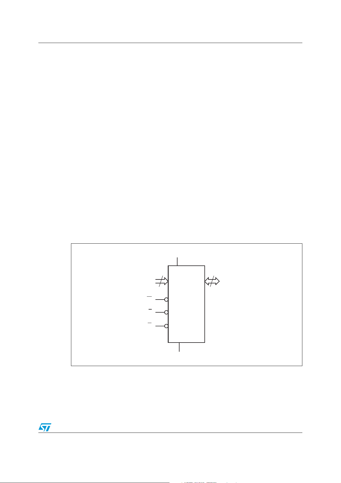
Figure 1. Logic diagram . . . . . . . . . . . . . . . . . . . . . . . . . . . . . . . . . . . . . . . . . . . . . . . . . . . . . . . . . . . . 5
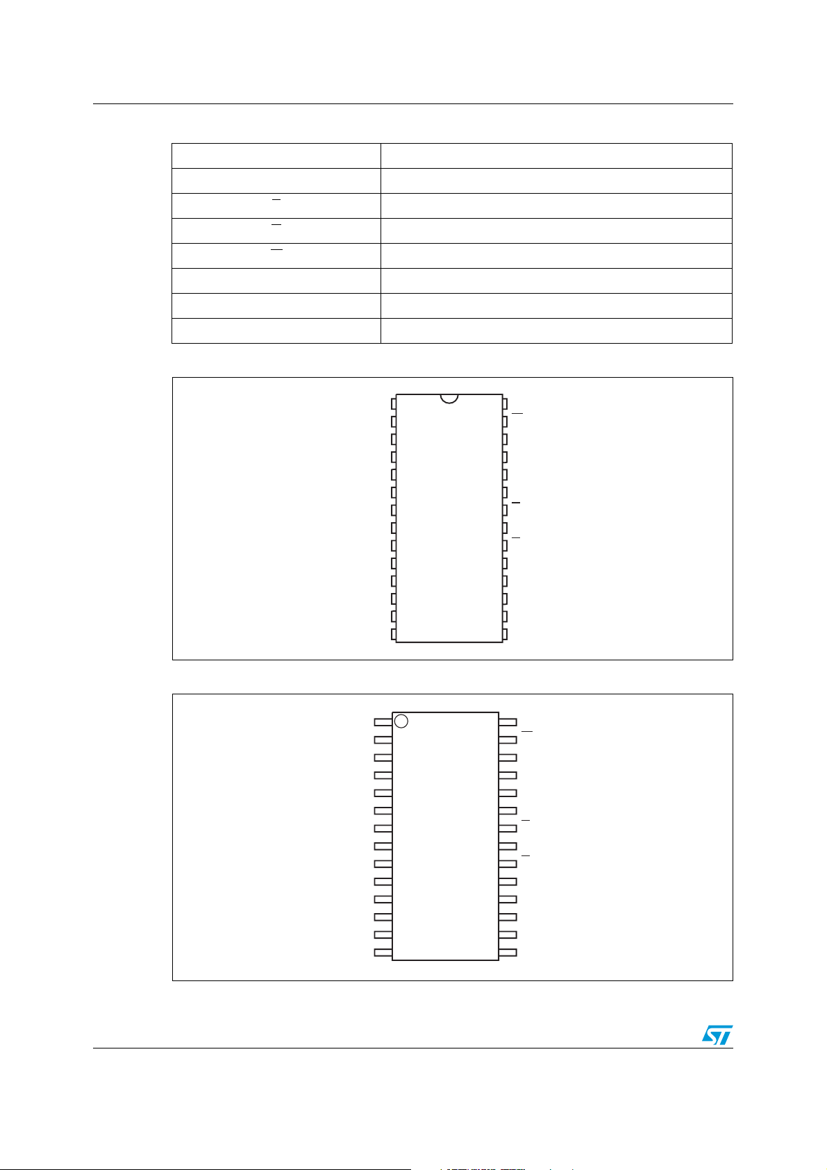
Figure 2. DIP connections . . . . . . . . . . . . . . . . . . . . . . . . . . . . . . . . . . . . . . . . . . . . . . . . . . . . . . . . . . 6
Figure 3. SOIC connections . . . . . . . . . . . . . . . . . . . . . . . . . . . . . . . . . . . . . . . . . . . . . . . . . . . . . . . . . 6
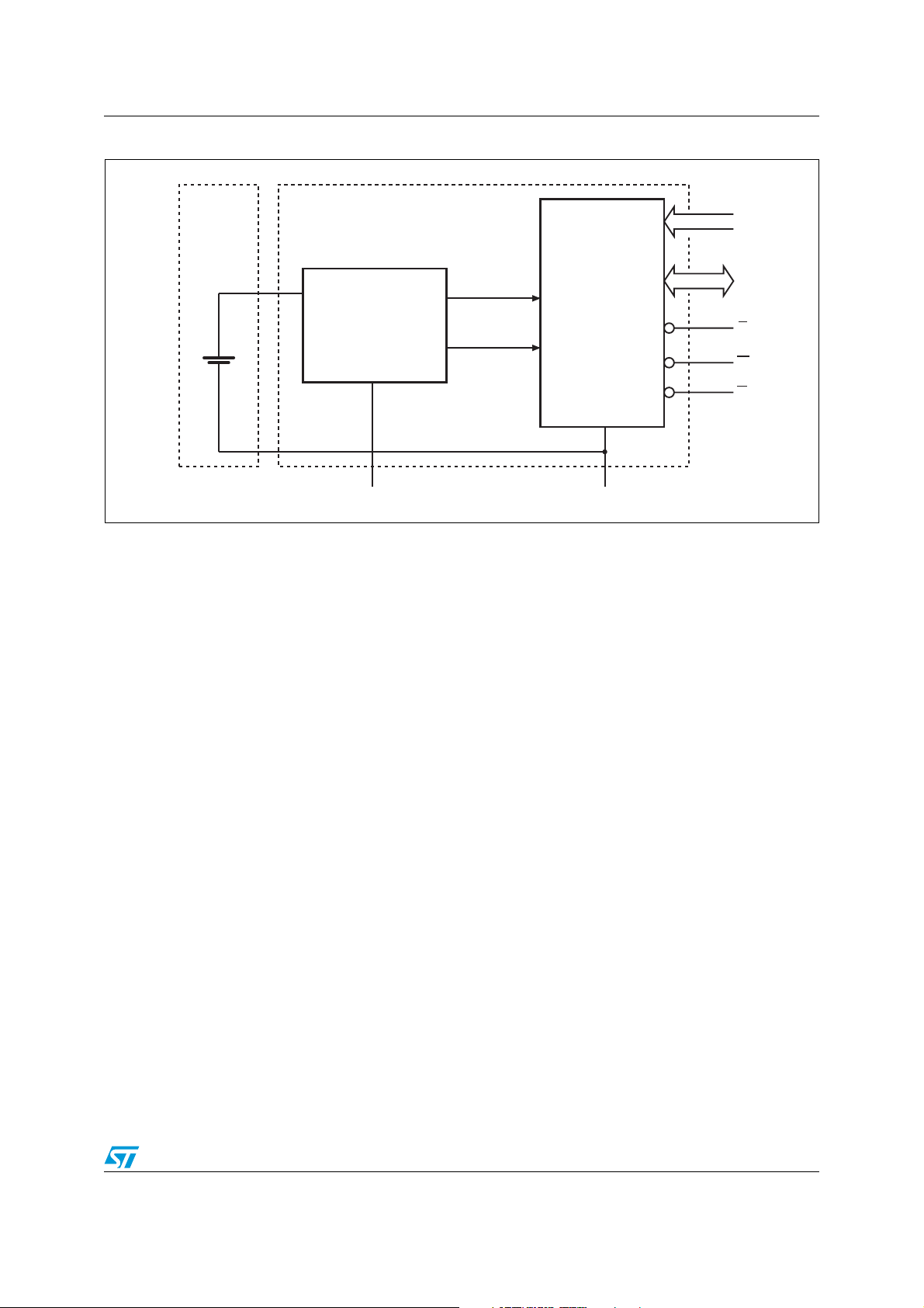
Figure 4. Block diagram . . . . . . . . . . . . . . . . . . . . . . . . . . . . . . . . . . . . . . . . . . . . . . . . . . . . . . . . . . . . 7
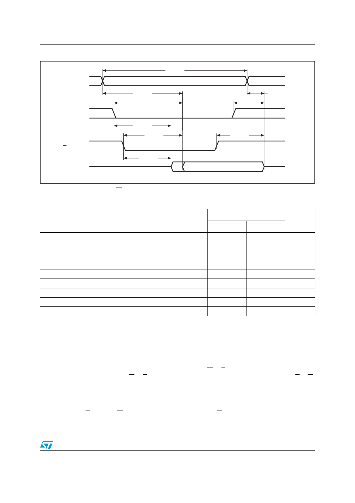
Figure 5. READ mode AC waveforms . . . . . . . . . . . . . . . . . . . . . . . . . . . . . . . . . . . . . . . . . . . . . . . . . 9
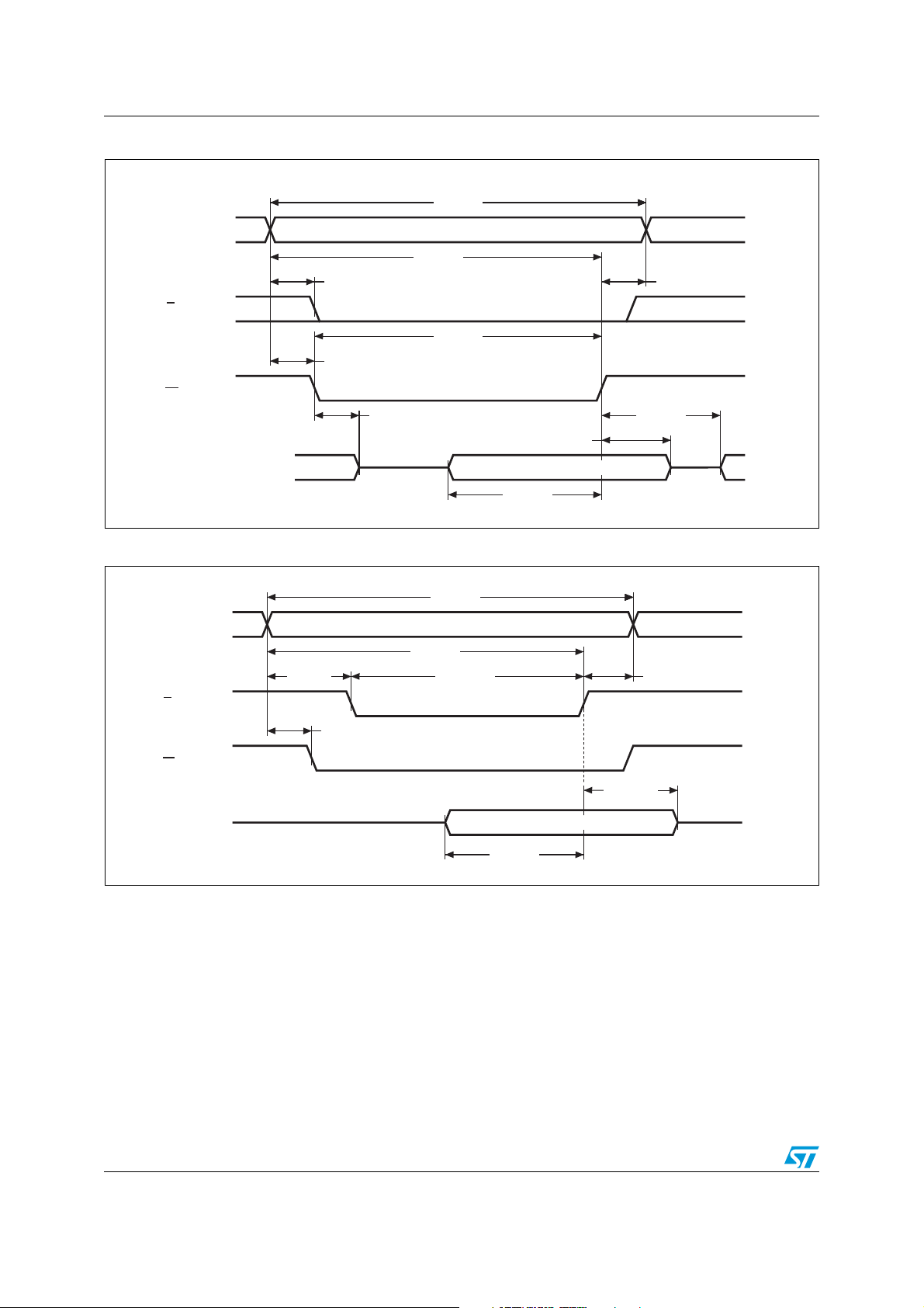
Figure 6. WRITE enable controlled, WRITE mode AC waveforms . . . . . . . . . . . . . . . . . . . . . . . . . . 10
Figure 7. Chip enable controlled, WRITE mode AC waveforms . . . . . . . . . . . . . . . . . . . . . . . . . . . . 10
Figure 8. Supply voltage protection . . . . . . . . . . . . . . . . . . . . . . . . . . . . . . . . . . . . . . . . . . . . . . . . . . 12
Figure 9. AC measurement load circuit . . . . . . . . . . . . . . . . . . . . . . . . . . . . . . . . . . . . . . . . . . . . . . . 14
Figure 10. Power down/up mode AC waveforms. . . . . . . . . . . . . . . . . . . . . . . . . . . . . . . . . . . . . . . . . 15
Figure 11. PCDIP28 – 28-pin plastic DIP, battery CAPHAT™, package outline . . . . . . . . . . . . . . . . . 17
Figure 12. SOH28 – 28-lead plastic small outline, battery SNAPHAT
Figure 13. SH – 4-pin SNAPHAT
Figure 14. SH – 4-pin SNAPHAT
Figure 15. Recycling symbols . . . . . . . . . . . . . . . . . . . . . . . . . . . . . . . . . . . . . . . . . . . . . . . . . . . . . . . 22
®
housing for 48 mAh battery, package outline . . . . . . . . . . . . . . . . 19
®
housing for 120 mAh battery, package outline . . . . . . . . . . . . . . . 20
®
, pack. outline. . . . . . . . . . . . . 18
4/24 Doc ID 2559 Rev 11
Page 5
M48Z58, M48Z58Y Description
1 Description
The M48Z58/Y ZEROPOWER® RAM is an 8 Kbit x 8 non-volatile static RAM that integrates
power-fail deselect circuitry and battery control logic on a single die. The monolithic chip is
available in two special packages to provide a highly integrated battery-backed memory
solution.
The M48Z58/Y is a non-volatile pin and function equivalent to any JEDEC standard 8 K x 8
SRAM. It also easily fits into many ROM, EPROM, and EEPROM sockets, providing the
non-volatility of PROMs without any requirement for special WRITE timing or limitations on
the number of WRITEs that can be performed.
The 28-pin, 600 mil DIP CAPHAT
button cell in a single package.
™
houses the M48Z58/Y silicon with a long life lithium
The 28-pin, 330 mil SOIC provides sockets with gold plated contacts at both ends for direct
connection to a separate SNAPHAT
®
housing containing the battery. The unique design
allows the SNAPHAT battery package to be mounted on top of the SOIC package after the
completion of the surface mount process. Insertion of the SNAPHAT housing after reflow
prevents potential battery damage due to the high temperatures required for device surfacemounting. The SNAPHAT housing is keyed to prevent reverse insertion.
The SOIC and battery packages are shipped separately in plastic anti-static tubes or in tape
& reel form.
For the 28-lead SOIC, the battery package (e.g., SNAPHAT) part number is “M4Z28BR00SH1”.
Figure 1. Logic diagram
V
CC
A0-A12
W
13
M48Z58
M48Z58Y
E
8
DQ0-DQ7
G
V
SS
Doc ID 2559 Rev 11 5/24
AI01176B
Page 6
Description M48Z58, M48Z58Y
Table 1. Signal names
A0-A12 Address inputs
DQ0-DQ7 Data inputs / outputs
E Chip enable input
G Output enable input
W WRITE enable input
V
CC
V
SS
NC Not connected internally
Figure 2. DIP connections
Supply voltage
Ground
NC V
1
A12
2
A7
3
A6
4
A5
5
A4
6
A3
7
8
9
10
11
M48Z58
M48Z58Y
A2
A1
A0
DQ0
12
DQ2
13
14
SS
28
27
26
25
24
23
22
21
20
19
18
17
16
15
CC
W
NC
A8
A9
A11
G
A10
E
DQ7
DQ6
DQ5DQ1
DQ4
DQ3V
AI01177B
Figure 3. SOIC connections
NC V
A12
A7
A6
A5
A4
A3
A2
A1
A0
DQ0
DQ2
SS
6/24 Doc ID 2559 Rev 11
1
2
3
4
5
6
7
8
9
10
11
12
13
14
M48Z58Y
28
27
26
25
24
23
22
21
20
19
18
17
16
15
CC
W
NC
A8
A9
A11
G
A10
E
DQ7
DQ6
DQ5DQ1
DQ4
DQ3V
AI01178B
Page 7
M48Z58, M48Z58Y Description
Figure 4. Block diagram
A0-A12
LITHIUM
CELL
VOLTAGE SENSE
AND
SWITCHING
CIRCUITRY
V
CC
POWER
V
PFD
8K x 8
SRAM ARRAY
V
SS
DQ0-DQ7
E
W
G
AI01394
Doc ID 2559 Rev 11 7/24
Page 8
Operating modes M48Z58, M48Z58Y
2 Operating modes
The M48Z58/Y also has its own power-fail detect circuit. The control circuitry constantly
monitors the single 5 V supply for an out of tolerance condition. When V
tolerance, the circuit write protects the SRAM, providing a high degree of data security in the
midst of unpredictable system operation brought on by low V
switchover voltage (V
), the control circuitry connects the battery which maintains data
SO
. As VCC falls below battery
CC
until valid power returns.
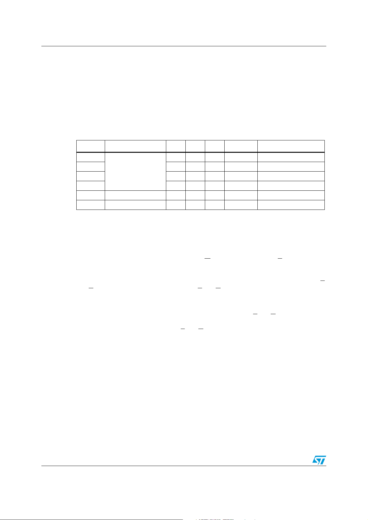
Table 2. Operating modes
Mode V
Deselect
WRITE V
READ V
READ V
Deselect V
Deselect ≤ V
1. See Table 10 on page 16 for details.
SO
CC
4.75 to 5.5 V
or
4.5 to 5.5 V
to V
PFD
SO
(min)
(1)
(1)
E G W DQ0-DQ7 Power
V
X X X High Z CMOS standby
X X X High Z Battery backup mode
X X High Z Standby
IH
XVILD
IL
V
IL
V
IL
V
IL
IH
IH
V
IH
IN
D
OUT
High Z Active
is out of
CC
Active
Active
Note: X = V
or VIL; VSO = Battery backup switchover voltage.
IH
2.1 READ mode
The M48Z58/Y is in the READ mode whenever W (WRITE enable) is high, E (chip enable) is
low. Thus, the unique address specified by the 13 address inputs defines which one of the
8,192 bytes of data is to be accessed. Valid data will be available at the data I/O pins within
address access time (t
and G
access times are also satisfied. If the E and G access times are not met, valid data
will be available after the latter of the chip enable access time (t
access time (t
The state of the eight three-state data I/O signals is controlled by E
activated before t
the address inputs are changed while E
for output data hold time (t
GLQV
) after the last address input signal is stable, providing that the E
AVQ V
) or output enable
ELQV
).
and G. If the outputs are
, the data lines will be driven to an indeterminate state until t
AVQ V
and G remain active, output data will remain valid
) but will go indeterminate until the next address access.
AXQX
AVQ V
. If
8/24 Doc ID 2559 Rev 11
Page 9
M48Z58, M48Z58Y Operating modes
Figure 5. READ mode AC waveforms
tAVAV
A0-A12
E
G
DQ0-DQ7
Note: WRITE enable (W
tAVQV tAXQX
tELQV
tELQX
tGLQV
tGLQX
) = High.
VAL ID
tEHQZ
tGHQZ
VAL ID
Table 3. READ mode AC characteristics
Symbol Parameter
t
AVAV
t
AVQ V
t
ELQV
t
GLQV
t
ELQX
t
GLQX
t
EHQZ
t
GHQZ
t
AXQX
1. Valid for ambient operating temperature: TA = 0 to 70 °C; VCC = 4.75 to 5.5 V or 4.5 to 5.5 V (except where noted).
2. CL = 5 pF (see Figure 9 on page 14).
READ cycle time 70 ns
Address valid to output valid 70 ns
Chip enable low to output valid 70 ns
Output enable low to output valid 35 ns
(2)
Chip enable low to output transition 5 ns
(2)
Output enable low to output transition 5 ns
(2)
Chip enable high to output Hi-Z 25 ns
(2)
Output enable high to output Hi-Z 25 ns
Address transition to output transition 10 ns
(1)
M48Z58/Y
Min Max
AI01385
Unit
2.2 WRITE mode
The M48Z58/Y is in the WRITE mode whenever W and E are low. The start of a WRITE is
referenced from the latter occurring falling edge of W
earlier rising edge of W
must return high for a minimum of t
to the initiation of another READ or WRITE cycle. Data-in must be valid t
end of WRITE and remain valid for t
cycles to avoid bus contention; although, if the output bus has been activated by a low on E
and G
, a low on W will disable the outputs t
or E. A WRITE is terminated by the
or E. The addresses must be held valid throughout the cycle. E or W
from chip enable or t
EHAX
afterward. G should be kept high during WRITE
WHDX
after W falls.
WLQZ
Doc ID 2559 Rev 11 9/24
from WRITE enable prior
WHAX
DVW H
prior to the
Page 10
Operating modes M48Z58, M48Z58Y
Figure 6. WRITE enable controlled, WRITE mode AC waveforms
tAVAV
A0-A12
tAVEL
E
tAVWL
W
tWLQZ
DQ0-DQ7
VAL ID
tAVWH
tWLWH
tWHDX
DATA INPUT
tDVWH
Figure 7. Chip enable controlled, WRITE mode AC waveforms
tAVAV
A0-A12
tAVEL
VAL ID
tAVEH
tELEH
tWHAX
tWHQX
AI01386
tEHAX
E
W
DQ0-DQ7
tAVWL
tDVEH
tEHDX
DATA INPUT
AI01387B
10/24 Doc ID 2559 Rev 11
Page 11
M48Z58, M48Z58Y Operating modes
Table 4. WRITE mode AC characteristics
Symbol Parameter
(1)
M48Z58/Y
Unit
Min Max
t
AVAV
t
AVW L
t
AVEL
t
WLWH
t
ELEH
t
WHAX
t
EHAX
t
DVW H
t
DVE H
t
WHDX
t
EHDX
t
WLQZ
t
AVW H
t
AVEH
t
WHQX
1. Valid for ambient operating temperature: TA = 0 to 70 °C; VCC = 4.75 to 5.5 V or 4.5 to 5.5 V (except where
noted).
2. CL = 5 pF (see Figure 9 on page 14).
goes low simultaneously with W going low, the outputs remain in the high impedance state.
3. If E
WRITE cycle time 70 ns
Address valid to WRITE enable low 0 ns
Address valid to chip enable low 0 ns
WRITE enable pulse width 50 ns
Chip enable low to chip enable high 55 ns
WRITE enable high to address transition 0 ns
Chip enable high to address transition 0 ns
Input valid to WRITE enable high 30 ns
Input valid to chip enable high 30 ns
WRITE enable high to input transition 5 ns
Chip enable high to input transition 5 ns
(2)(3)
WRITE enable low to output Hi-Z 25 ns
Address valid to WRITE enable high 60 ns
Address valid to chip enable high 60 ns
(2)(3)
WRITE enable high to output transition 5 ns
2.3 Data retention mode
With valid VCC applied, the M48Z58/Y operates as a conventional BYTEWIDE™ static
RAM. Should the supply voltage decay, the RAM will automatically power-fail deselect, write
protecting itself when V
become high impedance, and all inputs are treated as “Don't care.”
Note: A power failure during a WRITE cycle may corrupt data at the currently addressed location,
but does not jeopardize the rest of the RAM's content. At voltages below V
user can be assured the memory will be in a write protected state, provided the V
is not less than t
. The M48Z58/Y may respond to transient noise spikes on VCC that reach
F
into the deselect window during the time the device is sampling V
of the power supply lines is recommended.
When V
drops below VSO, the control circuit switches power to the internal battery which
CC
preserves data. The internal button cell will maintain data in the M48Z58/Y for an
accumulated period of at least 10 years when V
As system power returns and V
power supply is switched to external V
exceeds V
PFD
(max).
For more information on battery storage life refer to the application note AN1012.
falls within the V
CC
rises above VSO, the battery is disconnected, and the
CC
(max), V
PFD
is less than VSO.
CC
. Normal RAM operation can resume t
CC
(min) window. All outputs
PFD
. Therefore, decoupling
CC
(min), the
PFD
rec
fall time
CC
after VCC
Doc ID 2559 Rev 11 11/24
Page 12
Operating modes M48Z58, M48Z58Y
2.4 VCC noise and negative going transients
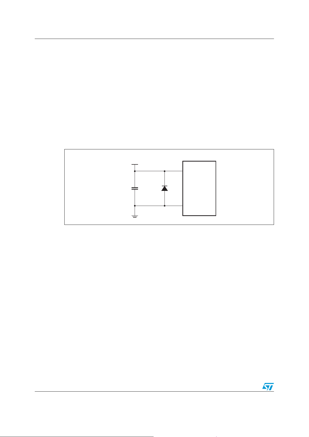
ICC transients, including those produced by output switching, can produce voltage
fluctuations, resulting in spikes on the V
capacitors are used to store energy which stabilizes the V
bypass capacitors will be released as low going spikes are generated or energy will be
absorbed when overshoots occur. A ceramic bypass capacitor value of 0.1 µF (see Figure 8)
is recommended in order to provide the needed filtering.
In addition to transients that are caused by normal SRAM operation, power cycling can
generate negative voltage spikes on V
one volt. These negative spikes can cause data corruption in the SRAM while in battery
backup mode. To protect from these voltage spikes, ST recommends connecting a schottky
diode from V
CC
to V
(cathode connected to VCC, anode to VSS). (Schottky diode 1N5817
SS
is recommended for through hole and MBRS120T3 is recommended for surface mount).
Figure 8. Supply voltage protection
V
CC
bus. These transients can be reduced if
CC
that drive it to values below VSS by as much as
CC
V
bus. The energy stored in the
CC
CC
0.1µF DEVICE
V
SS
AI02169
12/24 Doc ID 2559 Rev 11
Page 13
M48Z58, M48Z58Y Maximum ratings
3 Maximum ratings
Stressing the device above the rating listed in the absolute maximum ratings table may
cause permanent damage to the device. These are stress ratings only and operation of the
device at these or any other conditions above those indicated in the operating sections of
this specification is not implied. Exposure to absolute maximum rating conditions for
extended periods may affect device reliability.
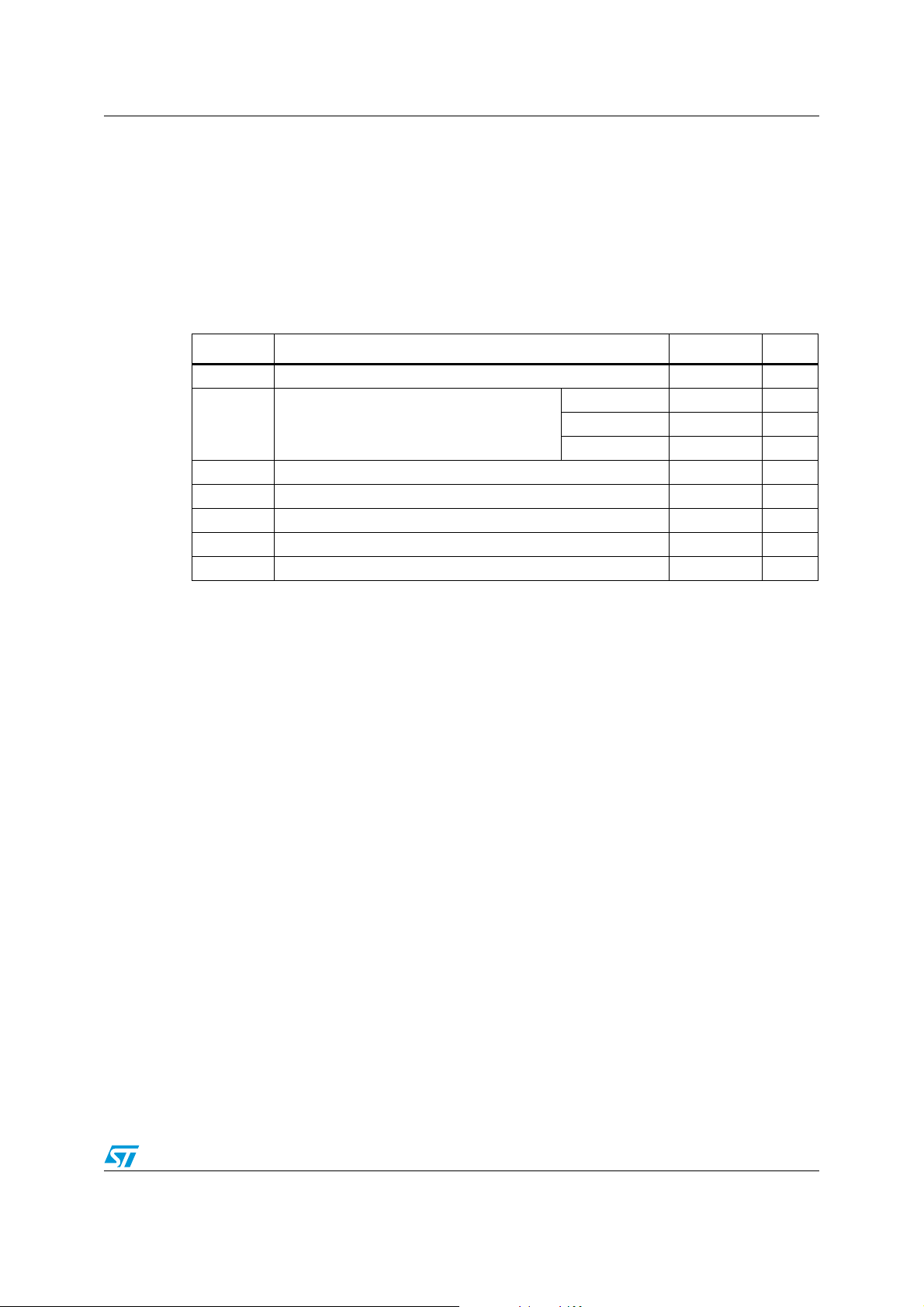
Table 5. Absolute maximum ratings
Symbol Parameter Value Unit
T
Ambient operating temperature 0 to 70 °C
A
SNAPHAT® top –40 to 85 °C
T
STG
Storage temperature (VCC off, oscillator off)
CAPHAT® DIP –40 to 85 °C
SOH28 –55 to 125 °C
(1)(2)
T
SLD
V
V
CC
I
O
P
1. For DIP package, soldering temperature of the IC leads is to not exceed 260 °C for 10 seconds.
Furthermore, the devices shall not be exposed to IR reflow nor preheat cycles (as performed as part of
wave soldering). ST recommends the devices be hand-soldered or placed in sockets to avoid heat damage
to the batteries.
2. For SOH28 package, lead-free (Pb-free) lead finish: reflow at peak temperature of 260 °C (the time above
255 °C must not exceed 30 seconds).
Lead solder temperature for 10 seconds 260 °C
Input or output voltages –0.3 to 7.0 V
IO
Supply voltage –0.3 to 7.0 V
Output current 20 mA
Power dissipation 1 W
D
Caution: Negative undershoots below –0.3 V are not allowed on any pin while in the battery backup
mode.
Caution: Do NOT wave solder SOIC to avoid damaging SNAPHAT
®
sockets.
Doc ID 2559 Rev 11 13/24
Page 14
DC and AC parameters M48Z58, M48Z58Y
4 DC and AC parameters
This section summarizes the operating and measurement conditions, as well as the DC and
AC characteristics of the device. The parameters in the following DC and AC characteristic
tables are derived from tests performed under the measurement conditions listed in Tabl e 6 :
Operating and AC measurement conditions. Designers should check that the operating
conditions in their projects match the measurement conditions when using the quoted
parameters.
Table 6. Operating and AC measurement conditions
Parameter M48Z58 M48Z58Y Unit
Supply voltage (VCC) 4.75 to 5.5 4.5 to 5.5 V
Ambient operating temperature (T
Load capacitance (CL) 100 100 pF
Input rise and fall times ≤ 5 ≤ 5ns
Input pulse voltages 0 to 3 0 to 3 V
Input and output timing ref. voltages 1.5 1.5 V
Note: Output Hi-Z is defined as the point where data is no longer driven.
) 0 to 70 0 to 70 °C
A
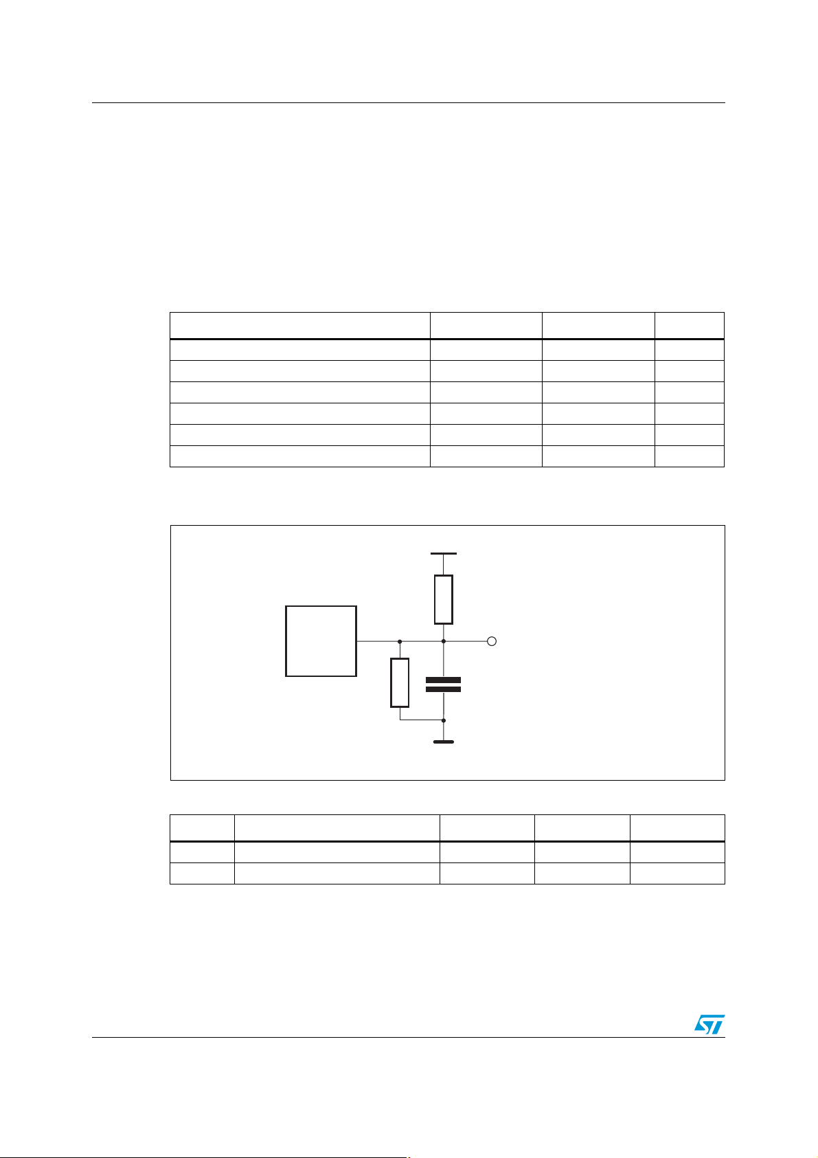
Figure 9. AC measurement load circuit
5V
1.9kΩ
DEVICE
UNDER
TEST
1kΩ
CL includes JIG capacitance
OUT
CL = 100pF or 5pF
Table 7. Capacitance
Symbol Parameter
C
C
IO
1. Effective capacitance measured with power supply at 5 V. Sampled only, not 100% tested.
2. At 25 °C, f = 1 MHz.
3. Outputs deselected.
Input capacitance - 10 pF
IN
(3)
Input / output capacitance - 10 pF
(1)(2)
Min Max Unit
AI01030
14/24 Doc ID 2559 Rev 11
Page 15
M48Z58, M48Z58Y DC and AC parameters
Table 8. DC characteristics
Symbol Parameter Test condition
(1)
Min Max Unit
I
I
LO
I
CC
I
CC1
I
CC2
V
V
V
V
LI
IL
IH
OL
OH
Input leakage current 0 V ≤ VIN ≤ V
(2)
Output leakage current 0 V ≤ V
OUT
≤ V
CC
CC
Supply current Outputs open 50 mA
Supply current (standby) TTL E = V
IH
Supply current (standby) CMOS E = VCC – 0.2 V 3 mA
Input low voltage –0.3 0.8 V
Input high voltage 2.2 VCC + 0.3 V
Output low voltage IOL = 2.1 mA 0.4 V
Output high voltage IOH = –1 mA 2.4 V
±1 µA
±1 µA
3mA
1. Valid for ambient operating temperature: TA = 0 to 70 °C; VCC = 4.75 to 5.5 V or 4.5 to 5.5 V (except where noted).
2. Outputs deselected.
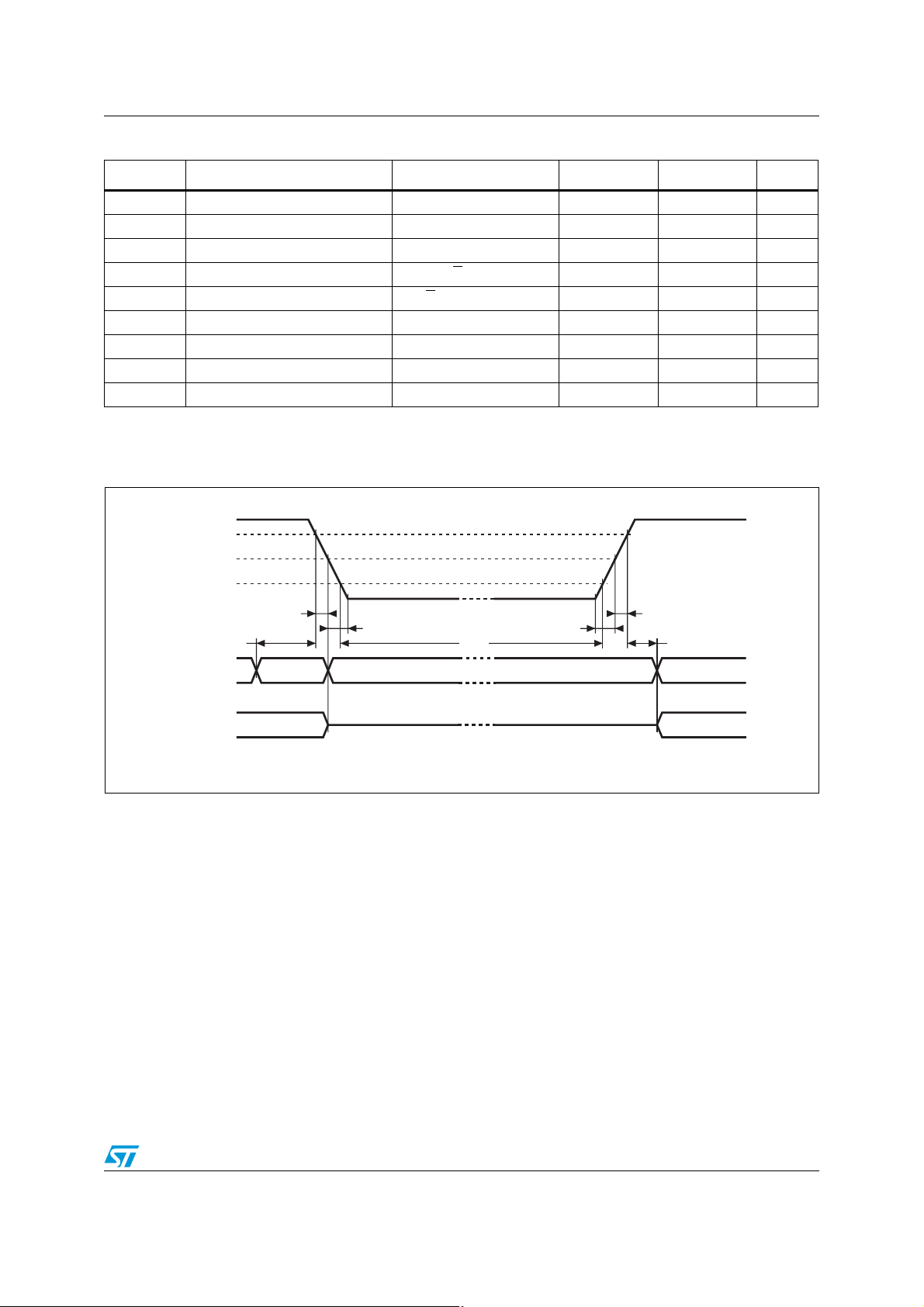
Figure 10. Power down/up mode AC waveforms
V
CC
V
(max)
PFD
V
(min)
PFD
VSO
INPUTS
tPD
tF
tFB
tDR
tRB
DON'T CARE
tR
trec
RECOGNIZEDRECOGNIZED
OUTPUTS
VAL ID VAL ID
(PER CONTROL INPUT)
HIGH-Z
(PER CONTROL INPUT)
Doc ID 2559 Rev 11 15/24
AI01168C
Page 16
DC and AC parameters M48Z58, M48Z58Y
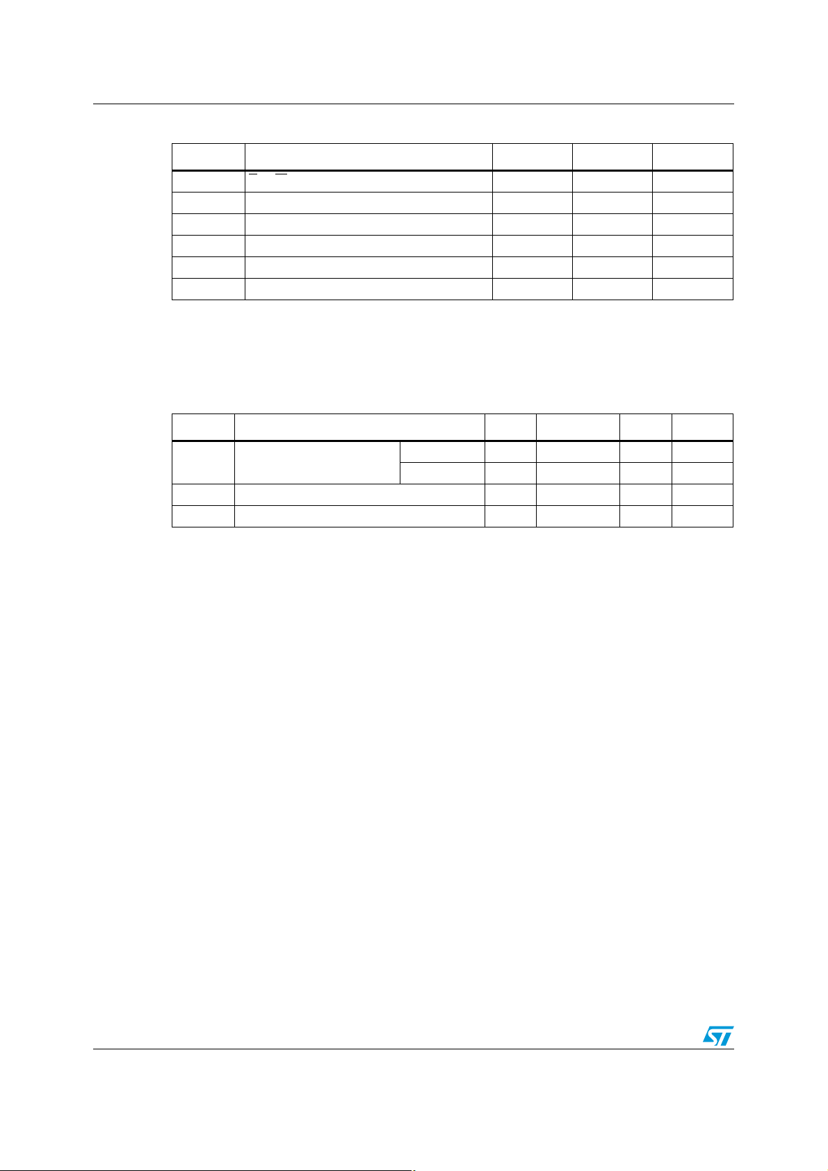
Table 9. Power down/up AC characteristics
Symbol Parameter
(1)
Min Max Unit
t
PD
(2)
t
F
t
FB
t
R
t
RB
t
rec
1. Valid for ambient operating temperature: TA = 0 to 70 °C; VCC = 4.75 to 5.5 V or 4.5 to 5.5 V (except where
noted).
2. V
PFD
until 200 µs after V
3. V
PFD
E or W at VIH before power down 0 µs
V
(max) to V
(3)
PFD
V
(min) to VSS VCC fall time 10 µs
PFD
V
(min) to V
PFD
VSS to V
V
PFD
(max) to V
(min) to VSS fall time of less than tFB may cause corruption of RAM data.
PFD
(min) V
PFD
(max) to inputs recognized 40 200 ms
(min) fall time of less than tF may result in deselection/write protection not occurring
passes V
CC
(min) VCC fall time 300 µs
PFD
(max) VCC rise time 10 µs
PFD
rise time 1 µs
CC
(min).
PFD
Table 10. Power down/up trip points DC characteristics
Symbol Parameter
V
V
t
DR
1. All voltages referenced to VSS.
2. Valid for ambient operating temperature: T
noted).
3. At 25 °C, VCC = 0 V.
Power-fail deselect voltage
PFD
Battery backup switchover voltage 3.0 V
SO
(3)
Expected data retention time 10 Years
(1)(2)
Min Typ Max Unit
M48Z58 4.5 4.6 4.75 V
M48Z58Y 4.2 4.35 4.5 V
= 0 to 70 °C; VCC = 4.75 to 5.5 V or 4.5 to 5.5 V (except where
A
16/24 Doc ID 2559 Rev 11
Page 17
M48Z58, M48Z58Y Package mechanical data
5 Package mechanical data
In order to meet environmental requirements, ST offers these devices in different grades of
ECOPACK
specifications, grade definitions and product status are available at: www.st.com.
ECOPACK
®
packages, depending on their level of environmental compliance. ECOPACK®
®
is an ST trademark.
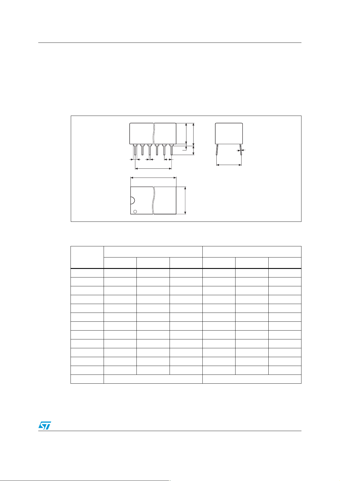
Figure 11. PCDIP28 – 28-pin plastic DIP, battery CAPHAT™, package outline
B1 B
Note: Drawing is not to scale.
Table 11. PCDIP28 – 28-pin plastic DIP, battery CAPHAT™, pack. mech. data
Symbol
Typ Mi n Ma x Typ Mi n Ma x
A2
A1AL
e1
e3
D
N
E
1
eA
mm inches
C
PCDIP
A 8.89 9.65 0.350 0.380
A1 0.38 0.76 0.015 0.030
A2 8.38 8.89 0.330 0.350
B 0.38 0.53 0.015 0.021
B1 1.14 1.78 0.045 0.070
C 0.20 0.31 0.008 0.012
D 39.37 39.88 1.550 1.570
E 17.83 18.34 0.702 0.722
e1 2.29 2.79 0.090 0.110
e3 33.02 1.3
eA 15.24 16.00 0.600 0.630
L 3.05 3.81 0.120 0.150
N28 28
Doc ID 2559 Rev 11 17/24
Page 18
Package mechanical data M48Z58, M48Z58Y
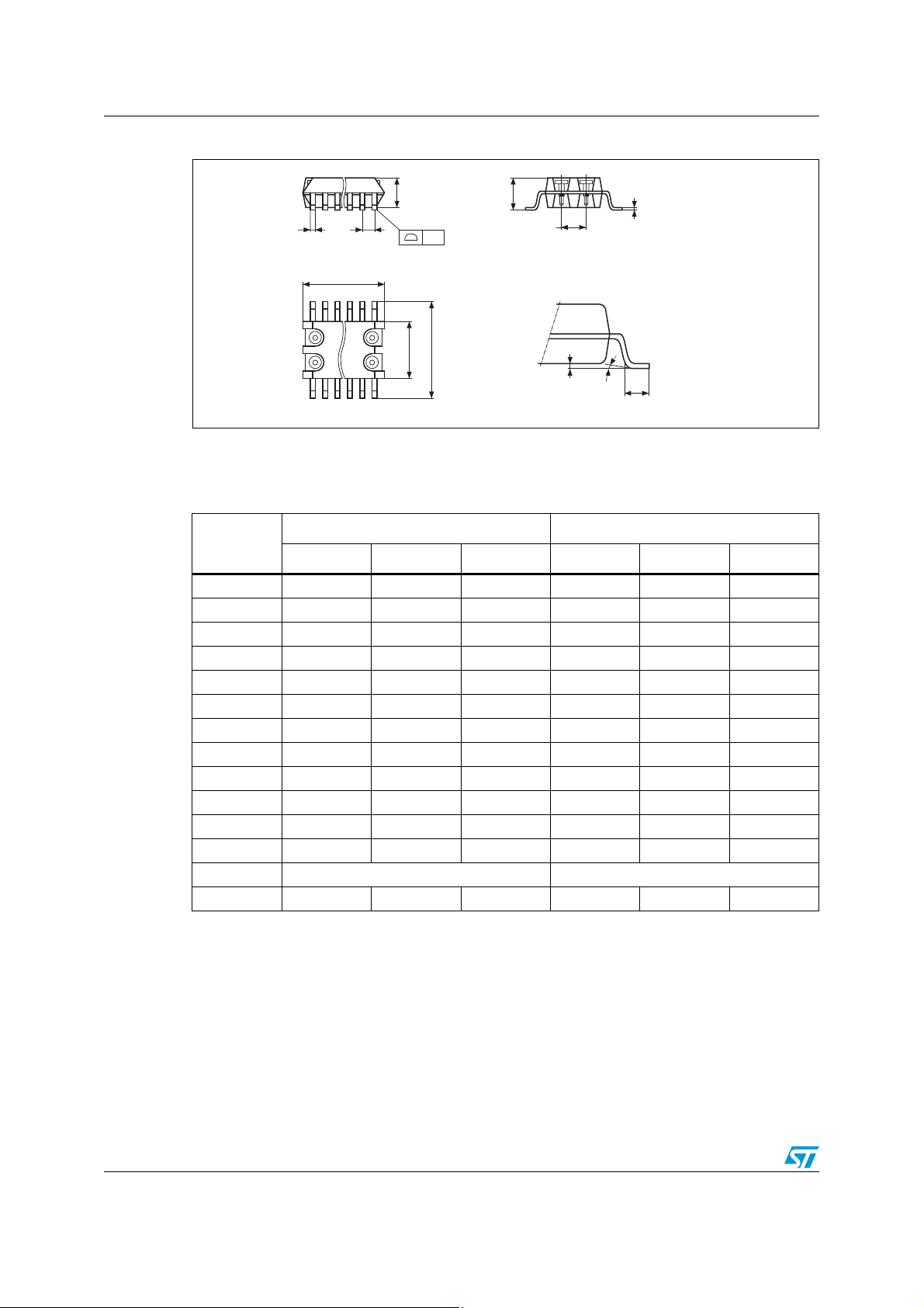
Figure 12. SOH28 – 28-lead plastic small outline, battery SNAPHAT®, pack. outline
Be
N
1
Note: Drawing is not to scale.
Table 12. SOH28 – 28-lead plastic small outline, battery SNAPHAT
data
Symbol
Typ Mi n Ma x Typ Mi n Ma x
A 3.05 0.120
A1 0.05 0.36 0.002 0.014
A2 2.34 2.69 0.092 0.106
B 0.36 0.51 0.014 0.020
C 0.15 0.32 0.006 0.012
D 17.71 18.49 0.697 0.728
E 8.23 8.89 0.324 0.350
e 1.27 – – 0.050 – –
eB 3.20 3.61 0.126 0.142
H 11.51 12.70 0.453 0.500
L 0.41 1.27 0.016 0.050
a0°8°0°8°
N28 28
CP 0.10 0.004
A2
CP
D
E
H
A
eB
C
LA1 α
SOH-A
®
, pack. mech.
mm inches
18/24 Doc ID 2559 Rev 11
Page 19
M48Z58, M48Z58Y Package mechanical data
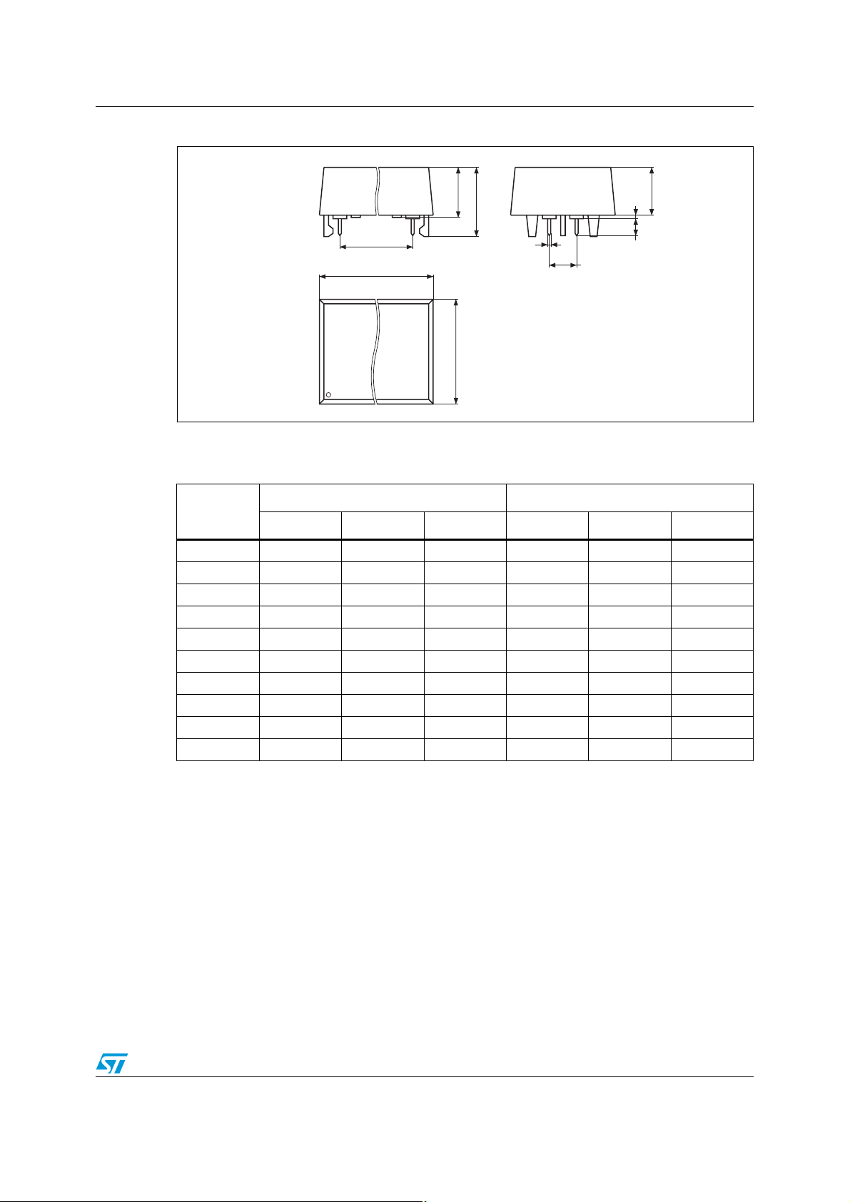
Figure 13. SH – 4-pin SNAPHAT® housing for 48 mAh battery, package outline
Note: Drawing is not to scale.
Table 13. SH – 4-pin SNAPHAT
Symbol
Typ Mi n Ma x Typ Mi n Ma x
A 9.78 0.385
A1 6.73 7.24 0.265 0.285
A2 6.48 6.99 0.255 0.275
A3 0.38 0.015
B 0.46 0.56 0.018 0.022
D 21.21 21.84 0.835 0.860
E 14.22 14.99 0.560 0.590
eA 15.55 15.95 0.612 0.628
eB 3.20 3.61 0.126 0.142
L 2.03 2.29 0.080 0.090
A1
A
eA
D
E
®
housing for 48 mAh battery, package mech. data
B
eB
A3
L
mm inches
A2
SHZP-A
Doc ID 2559 Rev 11 19/24
Page 20
Package mechanical data M48Z58, M48Z58Y
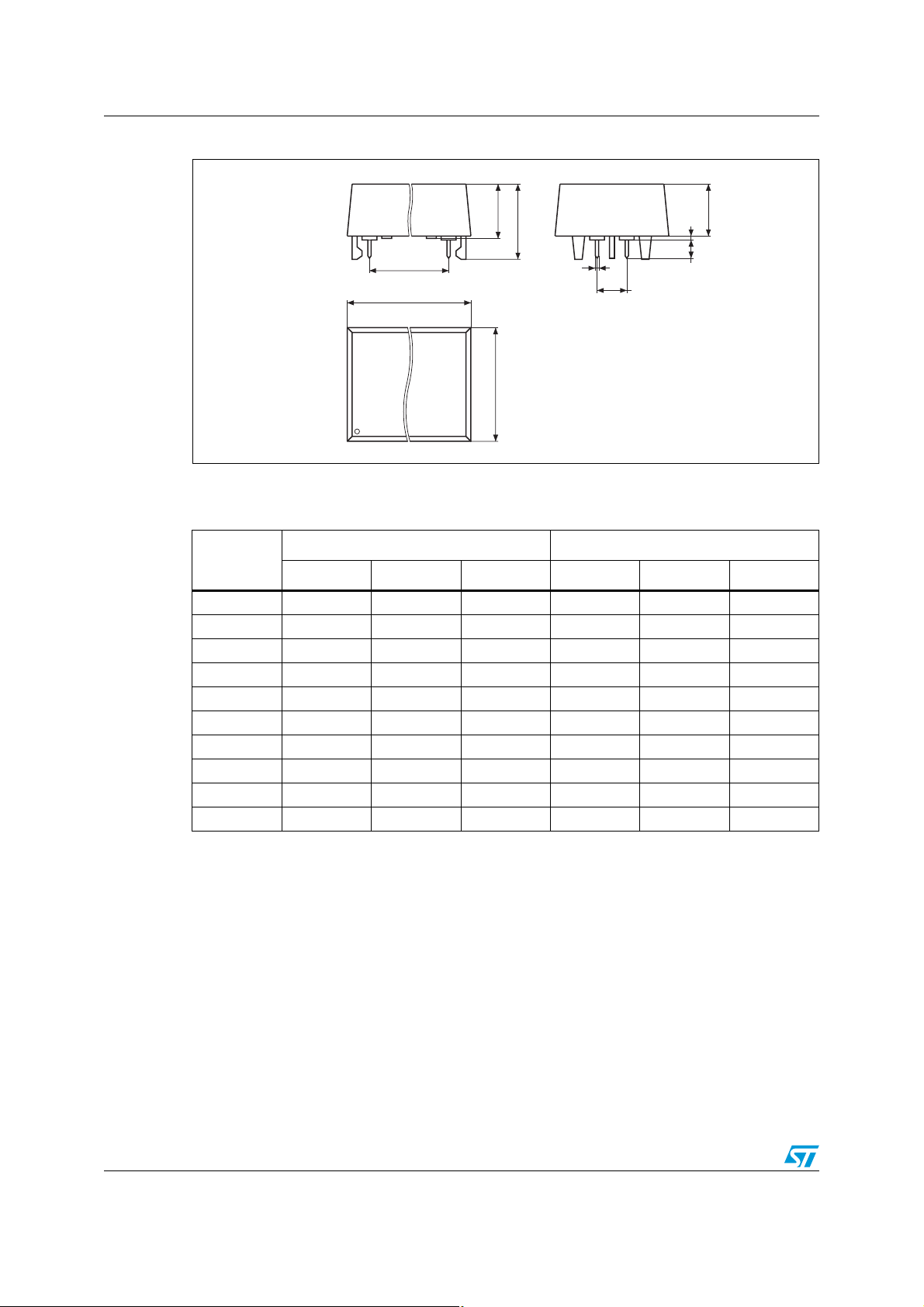
Figure 14. SH – 4-pin SNAPHAT® housing for 120 mAh battery, package outline
Note: Drawing is not to scale.
Table 14. SH – 4-pin SNAPHAT
Symb
Typ Mi n Ma x Typ Mi n Ma x
A 10.54 0.415
A1 8.00 8.51 0.315 0.335
A2 7.24 8.00 0.285 0.315
A3 0.38 0.015
B 0.46 0.56 0.018 0.022
D 21.21 21.84 0.835 0.860
E 17.27 18.03 0.680 0.710
eA 15.55 15.95 0.612 0.628
eB 3.20 3.61 0.126 0.142
L 2.03 2.29 0.080 0.090
A1
A
eA
D
E
®
housing for 120 mAh battery, pack. mech. data
B
eB
A3
L
mm inches
A2
SHZP-A
20/24 Doc ID 2559 Rev 11
Page 21
M48Z58, M48Z58Y Part numbering
6 Part numbering
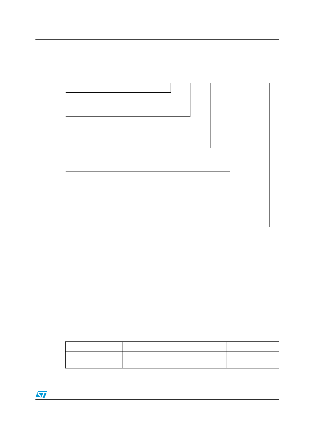
Table 15. Ordering information scheme
Example: M48Z 58Y –70 MH 1 E
Device type
M48Z
Supply voltage and write protect voltage
(1)
58
= VCC = 4.75 to 5.5 V; V
58Y = VCC = 4.5 to 5.5 V; V
Speed
–70 = 70 ns (for M48Z58/Y)
Package
PC = PCDIP28
(2)
= SOH28
MH
= 4.5 to 4.75 V
PFD
= 4.2 to 4.5 V
PFD
Temperature range
1 = 0 to 70°C
Shipping method
For SOH28:
®
E = ECOPACK
F = ECOPACK
package, tubes
®
package, tape & reel
For PCDIP28:
®
blank = ECOPACK
1. The M48Z58 part is offered with the PCDIP28 (ie., CAPHAT™) package only.
2. The SOIC package (SOH28) requires the SNAPHAT® battery package which is ordered separately under
the part number “M4Zxx-BR00SH1” in plastic tubes (see Table 16).
package, tubes
Caution: Do not place the SNAPHAT
drain the lithium button-cell battery.
For other options, or for more information on any aspect of this device, please contact the
ST sales office nearest you.
Table 16. SNAPHAT
Part number Description Package
M4Z28-BR00SH1 Lithium battery (48 mAh) SNAPHAT
M4Z32-BR00SH1 Lithium battery (120 mAh) SNAPHAT
®
battery table
®
battery package “M4Zxx-BR00SH1” in conductive foam as it will
®
®
SH
SH
Doc ID 2559 Rev 11 21/24
Page 22
Environmental information M48Z58, M48Z58Y
7 Environmental information
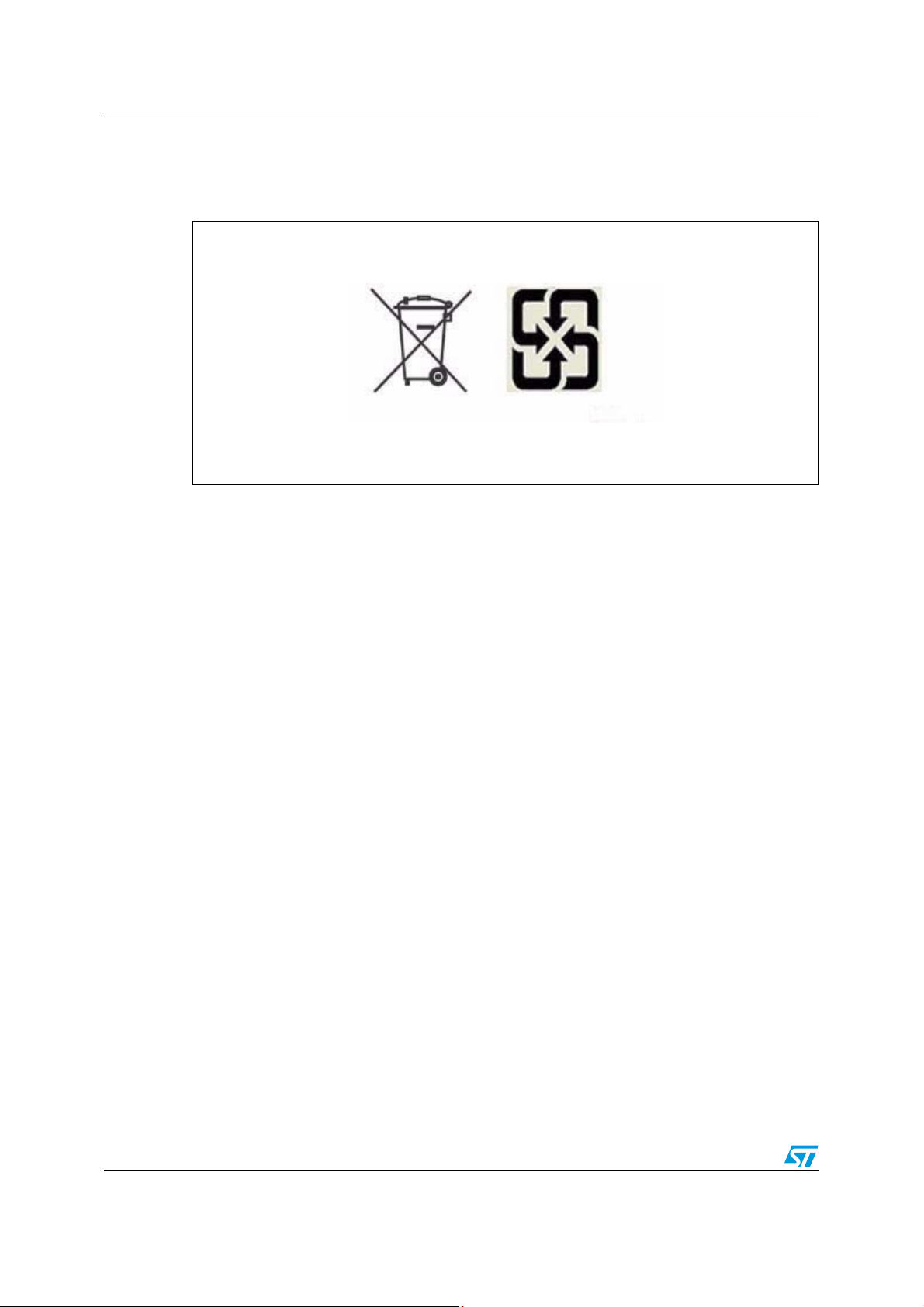
Figure 15. Recycling symbols
This product contains a non-rechargeable lithium (lithium carbon monofluoride chemistry)
button cell battery fully encapsulated in the final product.
Recycle or dispose of batteries in accordance with the battery manufacturer's instructions
and local/national disposal and recycling regulations.
22/24 Doc ID 2559 Rev 11
Page 23
M48Z58, M48Z58Y Revision history
8 Revision history
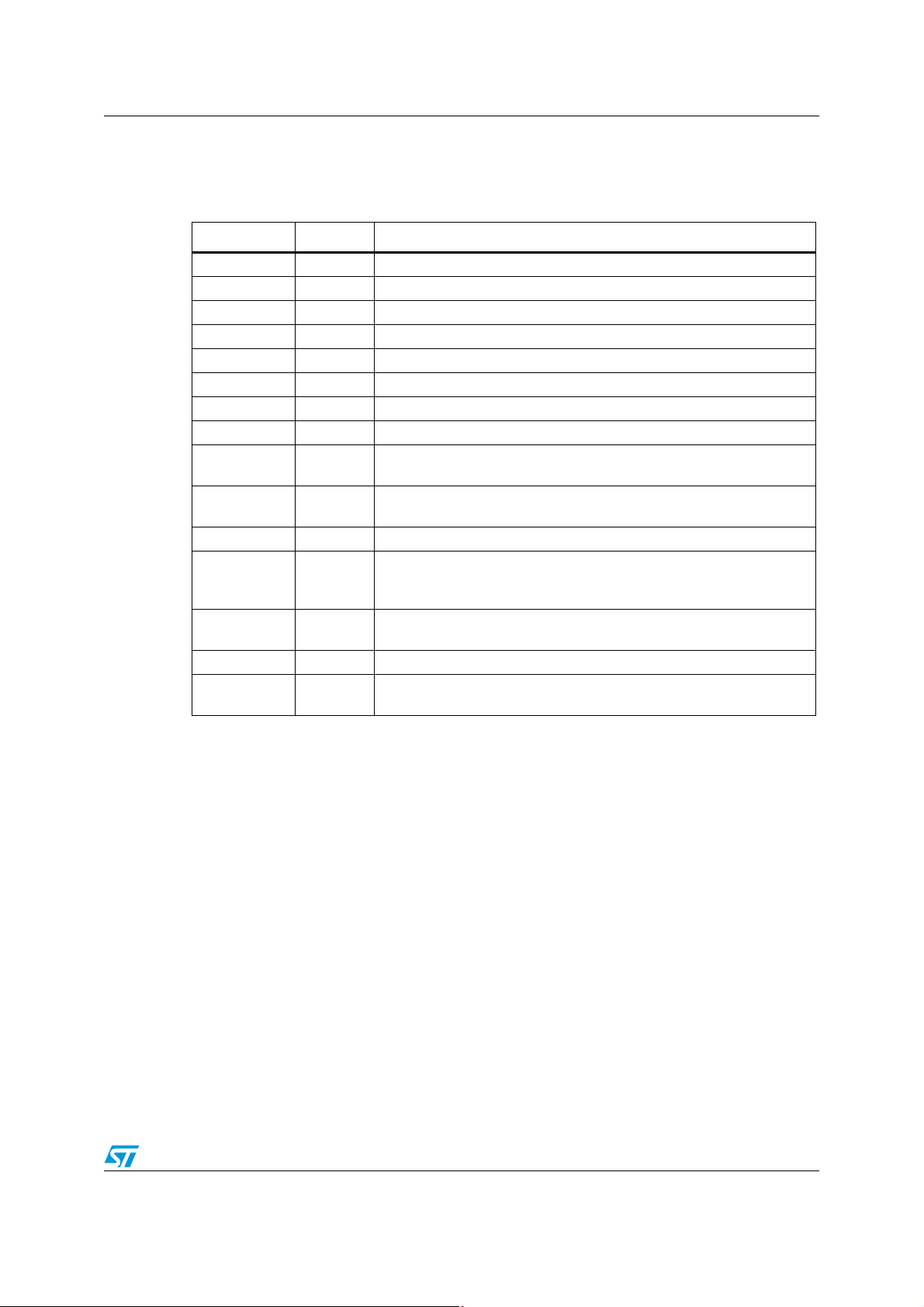
Table 17. Document revision history
Date Revision Changes
March 1999 1 First issue
10-Feb-2000 1.1 2-socket SOH and 2-pin SH packages removed
22-Feb-2000 1.2 Data retention mode paragraph changed
14-Sep-2001 2 Reformatted; added temperature information (Ta b le 7 , 8, 3, 4, 9, 10)
29-May-2002 2.1 Modify reflow time and temperature footnotes (Ta b le 5 )
16-Sep-2002 2.2 Remove footnote from ordering information (Ta bl e 1 5 )
02-Apr-2003 3 v2.2 template applied; test condition updated (Ta bl e 1 0)
23-Mar-2004 4 Reformatted; updated lead-free information (Ta bl e 5 , 15)
23-Nov-2004 5
09-Jun-2005 6
14-Dec-2005 7 Updated lead-free text (Ta b le 1 5)
06-Nov-2007 8
10-Mar-2009 9
14-Oct-2010 10 Updated Section 3, Ta b l e 11 ; reformatted document.
07-Jun-2011 11
Remove references to industrial temperature grade (Ta bl e 3 , 4, 5, 6, 8,
9, 10, 15)
®
Removal of SNAPHAT
4, 5, 6, 7, 8, 10, 15)
Reformatted; added lead-free second level interconnect information to
cover page and Section 5: Package mechanical data; updated Ta bl e 5 ,
15, 16.
Updated Ta b le 5 , text in Section 5: Package mechanical data; added
Section 7: Environmental information; minor reformatting.
Updated footnote 1 of Table 5: Absolute maximum ratings; updated
Section 7: Environmental information.
, industrial temperature sales types (Ta b le 3 ,
Doc ID 2559 Rev 11 23/24
Page 24

M48Z58, M48Z58Y
Please Read Carefully:
Information in this document is provided solely in connection with ST products. STMicroelectronics NV and its subsidiaries (“ST”) reserve the
right to make changes, corrections, modifications or improvements, to this document, and the products and services described herein at any
time, without notice.
All ST products are sold pursuant to ST’s terms and conditions of sale.
Purchasers are solely responsible for the choice, selection and use of the ST products and services described herein, and ST assumes no
liability whatsoever relating to the choice, selection or use of the ST products and services described herein.
No license, express or implied, by estoppel or otherwise, to any intellectual property rights is granted under this document. If any part of this
document refers to any third party products or services it shall not be deemed a license grant by ST for the use of such third party products
or services, or any intellectual property contained therein or considered as a warranty covering the use in any manner whatsoever of such
third party products or services or any intellectual property contained therein.
UNLESS OTHERWISE SET FORTH IN ST’S TERMS AND CONDITIONS OF SALE ST DISCLAIMS ANY EXPRESS OR IMPLIED
WARRANTY WITH RESPECT TO THE USE AND/OR SALE OF ST PRODUCTS INCLUDING WITHOUT LIMITATION IMPLIED
WARRANTIES OF MERCHANTABILITY, FITNESS FOR A PARTICULAR PURPOSE (AND THEIR EQUIVALENTS UNDER THE LAWS
OF ANY JURISDICTION), OR INFRINGEMENT OF ANY PATENT, COPYRIGHT OR OTHER INTELLECTUAL PROPERTY RIGHT.
UNLESS EXPRESSLY APPROVED IN WRITING BY AN AUTHORIZED ST REPRESENTATIVE, ST PRODUCTS ARE NOT
RECOMMENDED, AUTHORIZED OR WARRANTED FOR USE IN MILITARY, AIR CRAFT, SPACE, LIFE SAVING, OR LIFE SUSTAINING
APPLICATIONS, NOR IN PRODUCTS OR SYSTEMS WHERE FAILURE OR MALFUNCTION MAY RESULT IN PERSONAL INJURY,
DEATH, OR SEVERE PROPERTY OR ENVIRONMENTAL DAMAGE. ST PRODUCTS WHICH ARE NOT SPECIFIED AS "AUTOMOTIVE
GRADE" MAY ONLY BE USED IN AUTOMOTIVE APPLICATIONS AT USER’S OWN RISK.
Resale of ST products with provisions different from the statements and/or technical features set forth in this document shall immediately void
any warranty granted by ST for the ST product or service described herein and shall not create or extend in any manner whatsoever, any
liability of ST.
ST and the ST logo are trademarks or registered trademarks of ST in various countries.
Information in this document supersedes and replaces all information previously supplied.
The ST logo is a registered trademark of STMicroelectronics. All other names are the property of their respective owners.
© 2011 STMicroelectronics - All rights reserved
STMicroelectronics group of companies
Australia - Belgium - Brazil - Canada - China - Czech Republic - Finland - France - Germany - Hong Kong - India - Israel - Italy - Japan -
Malaysia - Malta - Morocco - Philippines - Singapore - Spain - Sweden - Switzerland - United Kingdom - United States of America
www.st.com
24/24 Doc ID 2559 Rev 11
 Loading...