

Page 1
3.3V, 256 Kbit (32 Kbit x 8) ZEROPOWER® SRAM
FEATURES SUMMARY
■ INTEGRATED, ULTRA LOW POWER SRAM,
and POWER-FAIL CONTROL CIRCUIT
■ READ CYCLE TIME EQUALS WRITE CYCLE
TIME
■ AUTOMATIC POWER-FAIL CHIP DESELECT
and WRITE PROTECTION
■ WRITE PROTECT VOLTAGES:
= Power-fail Deselect Voltage)
(V
PFD
– M48Z32V: 2.7V ≤ V
■ ULTRA-LOW STANDBY CURRENT
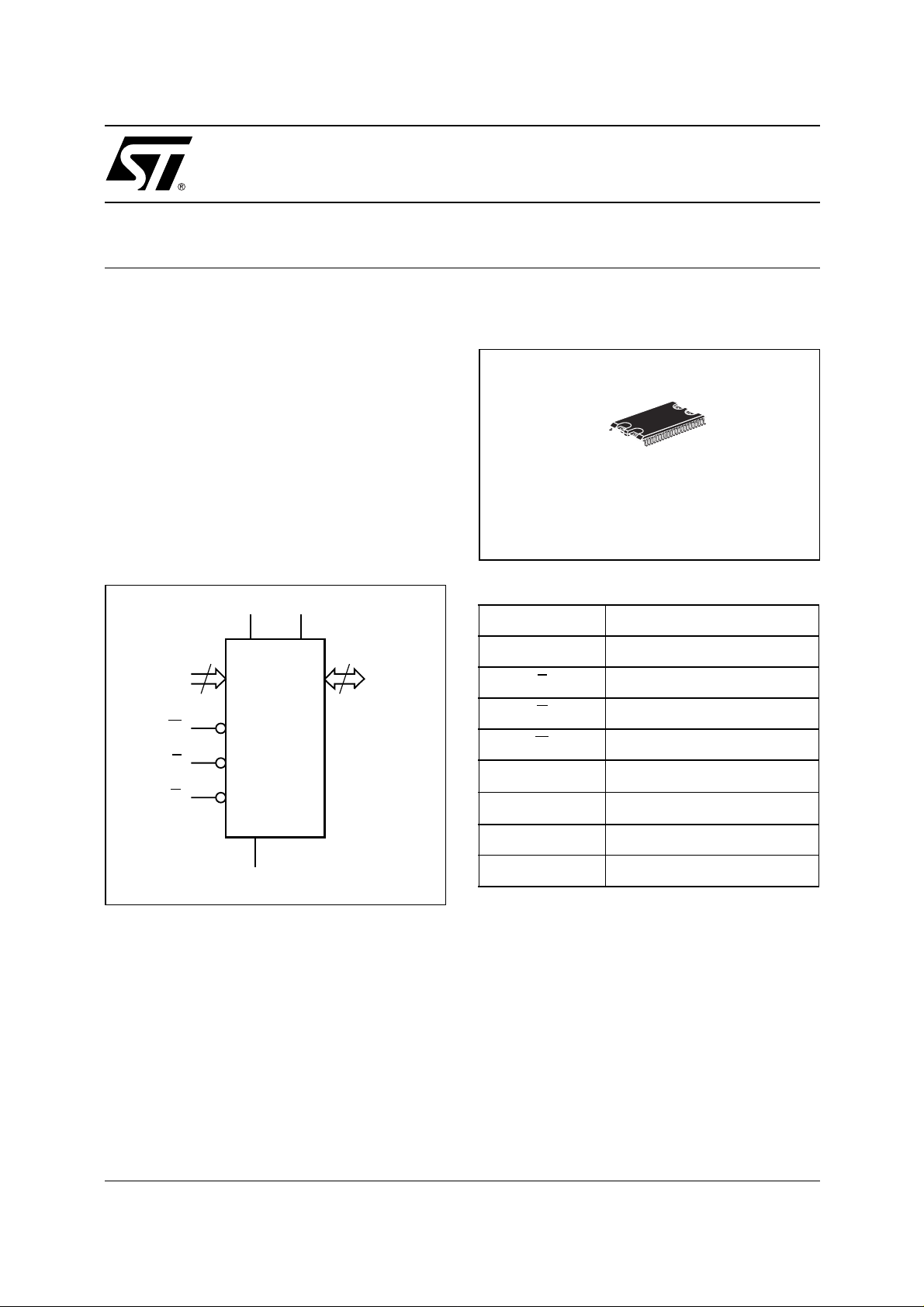
Figure 1. Logic Diagram
V
CC
PFD
≤ 3.0V
B +
M48Z32V
Figure 2. 44-pin, Hatless SOIC Package
44
1
SOH44 (MT)
Table 1. Signal Names
A0-A14 Address Inputs
A0-A14
W
15
M48Z32V
E
G
V
SS
8
DQ0-DQ7
AI04787
DQ0-DQ7 Data Inputs / Outputs
E
G
W
V
CC
V
SS
B + Positive Battery Pin
NC Not Connected
Chip Enable Input
Output Enable Input
WRITE Enable Input
Supply Voltage
Ground
1/16November 2002
Page 2

M48Z32V
TABLE OF CONTENTS
DESCRIPTION . . . . . . . . . . . . . . . . . . . . . . . . . . . . . . . . . . . . . . . . . . . . . . . . . . . . . . . . . . . . . . . . . . . . 3
SOIC Connections (Figure 3.) . . . . . . . . . . . . . . . . . . . . . . . . . . . . . . . . . . . . . . . . . . . . . . . . . . . . . . 3
Block Diagram (Fi g ure 4 .) . . . . . . . . . . . . . . . . . . . . . . . . . . . . . . . . . . . . . . . . . . . . . . . . . . . . . . . . . 4
MAXIMUM RATING. . . . . . . . . . . . . . . . . . . . . . . . . . . . . . . . . . . . . . . . . . . . . . . . . . . . . . . . . . . . . . . . . 4
Absolute Maximum Rati ng s (Table 2.) . . . . . . . . . . . . . . . . . . . . . . . . . . . . . . . . . . . . . . . . . . . . . . .4
DC AND AC PARAMETERS. . . . . . . . . . . . . . . . . . . . . . . . . . . . . . . . . . . . . . . . . . . . . . . . . . . . . . . . . . 5
Operating and AC Measurement Conditions (Table 3.) . . . . . . . . . . . . . . . . . . . . . . . . . . . . . . . . . . 5
AC Measurement Load Circuit (Figure 5.). . . . . . . . . . . . . . . . . . . . . . . . . . . . . . . . . . . . . . . . . . . . .5
Capacitance (Table 4.) . . . . . . . . . . . . . . . . . . . . . . . . . . . . . . . . . . . . . . . . . . . . . . . . . . . . . . . . . . . 5
DC Characteristi cs (Table 5.) . . . . . . . . . . . . . . . . . . . . . . . . . . . . . . . . . . . . . . . . . . . . . . . . . . . . . . 6
OPERATING MODES . . . . . . . . . . . . . . . . . . . . . . . . . . . . . . . . . . . . . . . . . . . . . . . . . . . . . . . . . . . . . . . 6
Operating Modes (Table 6.) . . . . . . . . . . . . . . . . . . . . . . . . . . . . . . . . . . . . . . . . . . . . . . . . . . . . . . . . 6
READ Mode. . . . . . . . . . . . . . . . . . . . . . . . . . . . . . . . . . . . . . . . . . . . . . . . . . . . . . . . . . . . . . . . . . . . 7
READ Mode AC Waveforms (Figure 6.) . . . . . . . . . . . . . . . . . . . . . . . . . . . . . . . . . . . . . . . . . . . . . . 7
READ Mode AC Characteristic s (Table 7.) . . . . . . . . . . . . . . . . . . . . . . . . . . . . . . . . . . . . . . . . . . . . 8
WRITE Mode. . . . . . . . . . . . . . . . . . . . . . . . . . . . . . . . . . . . . . . . . . . . . . . . . . . . . . . . . . . . . . . . . . . 9
WRITE Enable Controlled, WRITE Mode AC Wav eforms (Figure 7.). . . . . . . . . . . . . . . . . . . . . . . .9
Chip Enable Controlled, WRITE Mode AC Waveforms (Figure 8.). . . . . . . . . . . . . . . . . . . . . . . . . . 9
WRITE Mode AC Characteristics (Table 8.) . . . . . . . . . . . . . . . . . . . . . . . . . . . . . . . . . . . . . . . . . . 10
Data Retention Mode. . . . . . . . . . . . . . . . . . . . . . . . . . . . . . . . . . . . . . . . . . . . . . . . . . . . . . . . . . . . 11
Power Down/Up Mode AC Waveforms (Figure 9.) . . . . . . . . . . . . . . . . . . . . . . . . . . . . . . . . . . . . . 11
Power Down/Up AC Characteristics (Table 9.) . . . . . . . . . . . . . . . . . . . . . . . . . . . . . . . . . . . . . . . . 11
Power Down/Up Trip Points DC Char ac te r i stics (Table 10.). . . . . . . . . . . . . . . . . . . . . . . . . . . . . . 12
V
Noise And Negative Going Transients. . . . . . . . . . . . . . . . . . . . . . . . . . . . . . . . . . . . . . . . . . .12
CC
Supply Voltage Protection (Figure 10.) . . . . . . . . . . . . . . . . . . . . . . . . . . . . . . . . . . . . . . . . . . . . . .1 2
PART NUMBERING . . . . . . . . . . . . . . . . . . . . . . . . . . . . . . . . . . . . . . . . . . . . . . . . . . . . . . . . . . . . . . . 13
PACKAGE MECHANICAL INFORMATION . . . . . . . . . . . . . . . . . . . . . . . . . . . . . . . . . . . . . . . . . . . . . 14
REVISION HISTORY . . . . . . . . . . . . . . . . . . . . . . . . . . . . . . . . . . . . . . . . . . . . . . . . . . . . . . . . . . . . . . . 15
2/16
Page 3
M48Z32V
DESCRIPTION
®
The M48Z32V ZEROPOWER
RAM is a 32 Kbit x
8, non-volatile static RAM that integrates powerfail deselect circuitry and battery control logic on a
single die.
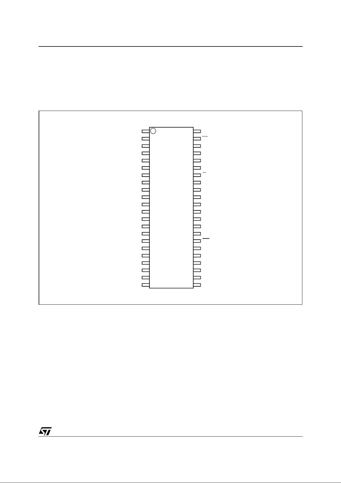
Figure 3. SOIC Connections
A14
A12
A7
A6
A5 A9
A4
NF
NC
NC
NC
NC
NC
NC
NC
A3
A2
A1
A0
DQ1
DQ2
V
SS
1
2
3
4
5
6
7
8
9
10
11
12
13
14
15
16
17
18
19
20
21
22
The 44-pin, 330mil SOIC provides a battery pin for
an external, user-supplied battery. T his is all that
is required to fully non-volatize the SRAM.
44
V
CC
43
W
42
A13
41
A8
40
39
A11
38
G
37
NC
36
NC
35
NC
34
M48Z32V
33
32
31
30
29
28
27
26
25
24
23
NC
NC
NC
NC
A10
CE
DQ7
DQ6
DQ5DQ0
DQ4
DQ3
B +
Note: NF, Pin 7 must be tied to VSS.
AI04786
3/16
Page 4
M48Z32V
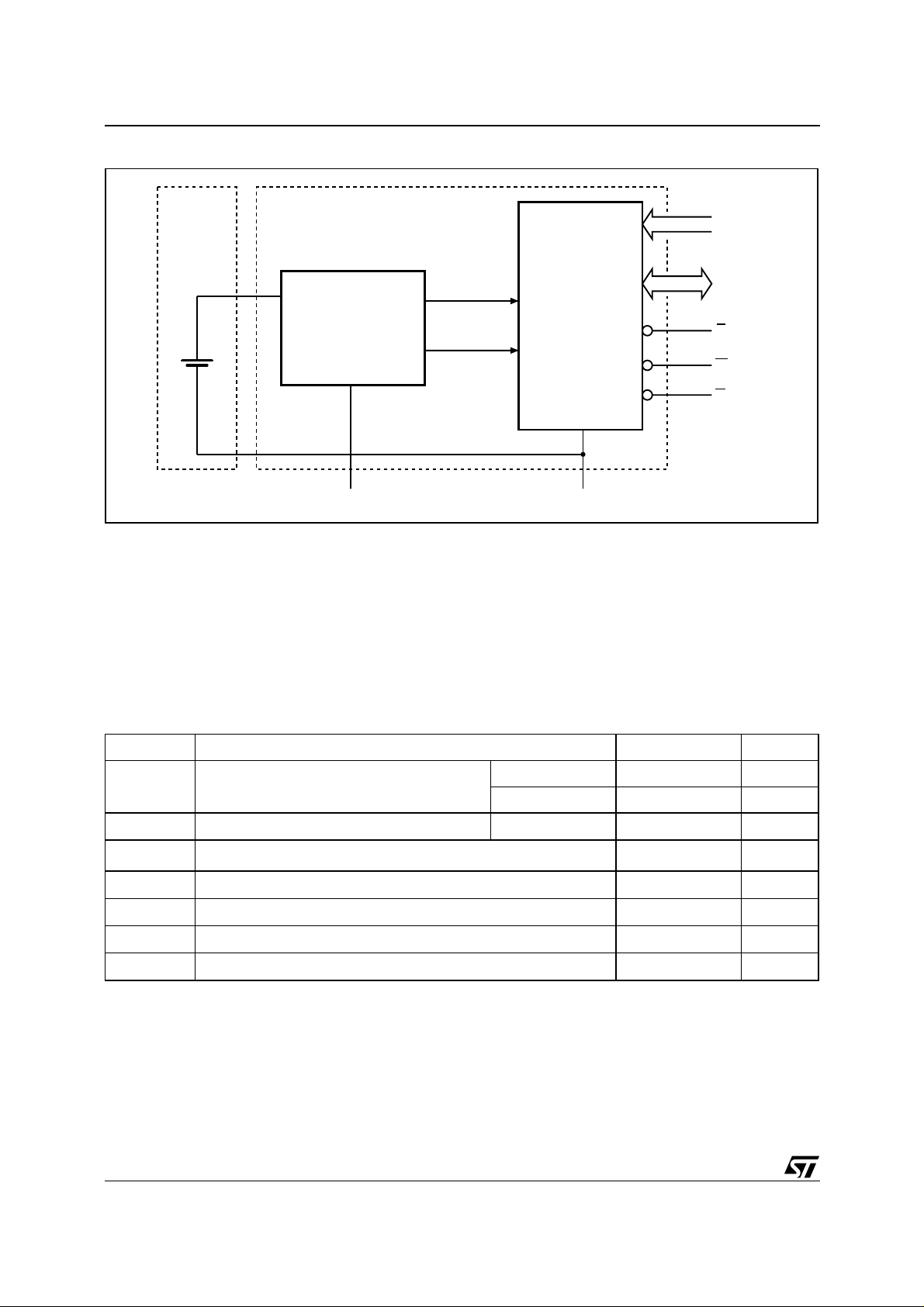
Figure 4. Block Diagram
A0-A14
LITHIUM
CELL
VOLTAGE SENSE
AND
SWITCHING
CIRCUITRY
USER
SUPPLIED
V
CC
MAXIMUM RATI N G
Stressing the device above the rating l isted in the
“Absolute Maximum Ratings” table may cause
permanent damage to the device. These are
stress ratings only and operation of the dev ice at
these or any other conditions above those indicated in the Operating sections of this specification is
POWER
V
PFD
32K x 8
SRAM ARRAY
V
SS
DQ0-DQ7
E
W
G
AI04788
not implied. Exposure to Absol ute Maxim um Rating conditions for extended periods may affect device reliability. Refer also to the
STMicroelectronics SURE Program and oth er relevant quality documents.
Table 2. Absolute Maximum Ratings
Symbol Parameter Value Unit
T
A
T
STG
T
SLD
V
IO
V
CC
I
O
P
D
Note: 1. Reflow at peak temperature of 215°C to 225°C for < 60 seconds (total thermal budget not to exceed 180°C for between 90 and 120
Ambient Operating Temperature
Storage Temperature (VCC Off, Oscillator Off)
(1)
Lead Solder Temperature for 10 seconds 260 °C
Input or Output Voltages
Supply Voltage –0.3 to 4.6 V
Output Current 20 mA
Power Dissipation 1 W
seconds).
CAUTION: Negative undershoots be l ow –0.3V are not allowed on a ny pin while i n th e Battery Ba ck -up mode.
Grade 1 0 to 70 °C
Grade 6 –40 to 85 °C
SOIC –55 to 125 °C
–0.3 to V
CC
+ 0.3
V
4/16
Page 5
DC AND AC PARAMETERS
This section summarizes the operat ing and measurement conditions, as well as the DC and AC
characteristics of the device. The parameters in
the following DC and AC Characteristic tables are
derived from tests performed under the M easure-
Table 3. Operating and AC Measurement Conditions
(1)
Supply Voltage (V
CC
)
Ambient Operating Temperature (T
Parameter
)
A
M48Z32V
ment Conditions listed i n the relevant tables. Designers should check that the operating conditions
in their projects match the measurement conditions when using the quoted parameters.
M48Z32V Unit
3.0 to 3.6 V
Grade 1 0 to 70 °C
Grade 6 –40 to 85 °C
Load Capacitance (C
)
L
50
pF
Input Rise and Fall Times ≤ 5ns
Input Pulse Voltages 0 to 3 V
Input and Output Timing Ref. Voltages 1.5 V
Note: 1. Out put Hi-Z is de fined as the point where da ta is no l onger driven.
Figure 5. AC Me asureme nt Load Circui t
DEVICE
UNDER
TEST
CL includes JIG capacitance
645Ω
CL = 50pF or
5pF
1.75V
AI04789
Table 4. Capacitance
Symbol
C
IN
C
IO
Note: 1. Eff ective capa citance measured with power supply at 3.3V; sam pled only, not 100% test ed.
2. At 25°C, f = 1MHz.
3. Outputs desel ected.
Input Capacitance 10 pF
(3)
Input / Output Capacitance 10 pF
Parameter
(1,2)
Min Max Unit
5/16
Page 6

M48Z32V
Table 5. DC Characteristics
Sym Parameter
Test Condition
(1)
Min Typ Max Unit
Input Leakage Current
I
LI
(2)
I
V
Note: 1. Va l i d fo r Ambient Op erating Temperature : TA = 0 to 70°C or –40 to 85°C; VCC = 3.0 to 3.6V (except where noted).
Output Leakage Curren t
LO
I
Battery Current
BAT
I
Supply Current
CC1
Supply Current (TTL
I
CC2
Standby)
Supply Current (CMOS
I
CC3
Standby)
(3)
Input Low Voltage –0.3 0.8 V
IL
V
Input High Voltage 2.2
IH
V
Output Low Voltage
OL
V
Output High Voltage
OH
2. Outputs desel ected.
3. Negati ve spikes of –1V al l o wed for up t o 10ns once per cycle.
0V ≤ V
0V ≤ V
T
= 40°C; VCC = 0V
A
= 0mA; Cycle Time = Min
I
O
E
= 0.2V, other input =
V
CC
= VCC – 0.2V
E
I
≤ V
IN
CC
≤ V
OUT
V
BAT
CC
= 3V
– 2V or 0.2V
= V
E
IH
= 2.1mA
OL
I
= –1mA 0.8V
OH
CC
±1 µA
±1 µA
0.2 1.2 µA
45 mA
800 µA
500 µA
V
+ 0.3
CC
0.4 V
OPERATING MODES
The M48Z32V also has its own Power-fail Detect
circuit. The control circuitry constantly monitors
the single power supply for an out of tolerance
condition. When V
is out of tolerance, the circuit
CC
write protects the SRAM, providing a high degree
of data security in the midst of unpredictable s ystem operation brought on by low V
below approximately V
, the control circuitry con-
SO
CC
nects the battery which maintains data until valid
power returns.
V
V
. As VCCfalls
Table 6. Operating Modes
Mode
Deselect
WRITE
READ
READ
Deselect
VSO to V
Deselect
Note: X = VIH or VIL; VSO = Battery B ack-up Switc hover Voltage.
1. See Table 10, page 12 for det ai l s.
6/16
V
CC
3.0 to 3.6V
(min)
PFD
(1)
≤ V
SO
(1)
E G W DQ0-DQ7 Power
V
IH
V
IL
V
IL
V
IL
X X X High Z CMOS Standby
X X X High Z Battery Back-up Mode
X X High Z Standby
X
V
IL
V
IH
V
IL
V
IH
V
IH
D
D
OUT
IN
Active
Active
High Z Active
Page 7

READ Mode
The M48Z32V is in the READ Mode wh enever W
(WRITE Enable) is high, E (Chip Enab le) is low.
The device architecture allows ripple-through access of data from eight of 262,144 locations in the
static storage array. Thus, the unique address
specified by the 15 Address Inputs defines which
one of the 32,768 bytes of data is to be accessed.
Valid data will be available at the Data I/O pins
within Address Access time (t
) after the last
AVQV
address input signal is stable, providing that the E
and G access times are also satisfied. If the E and
G
access times are not met, valid data will be
Figure 6. READ Mode AC Waveforms
available after the latter of the Chip Enable Access
time (t
(t
GLQV
) or Output Enable Access time
ELQV
).
The state of the eight t hree-s tate Da ta I/O s i gnals
is controlled by E
ed before t
indeterminate state until t
puts are changed while E
and G. If the outputs are activat-
, the data lines will be driven to an
AVQV
. If the Ad dres s In-
AVQV
and G remain active,
output dat a will r ema in valid for Outp ut Dat a Hold
time (t
) but will go indeterminate until the next
AXQX
Addr e ss Access.
tAVAV
M48Z32V
A0-A14
E
G
DQ0-DQ7
Note: WRITE Enable (W) = High.
VALID
tAVQV tAXQX
tELQV
tELQX
tGLQX
tGLQV
tGHQZ
VALID
tEHQZ
AI00925
7/16
Page 8

M48Z32V
Table 7. READ Mode AC Characteristics
Symbol
t
AVAV
t
AVQV
t
ELQV
t
GLQV
t
ELQX
t
GLQX
t
EHQZ
t
GHQZ
(2)
(2)
(2)
(2)
READ Cycle Time 35 ns
Address Valid to Output Valid 35 ns
Chip Enable Low to Output Valid 35 ns
Output Enable Low to Output Valid 15 ns
Chip Enable Low to Output Transition 5 ns
Output Enable Low to Output Transition 0 ns
Chip Enable High to Output Hi-Z 13 ns
Output Enable High to Output Hi-Z 13 ns
Parameter
(1)
M48Z32V
Unit–35
Min Max
t
AXQX
Note: 1. Va l i d fo r Ambient Op erating Temperature : TA = 0 to 70°C or –40 to 85°C; VCC = 3.0 to 3.6V (except where noted).
= 5pF (see Figure 5, page 5).
2. C
L
Address Transition to Output Transition 5 0 ns
8/16
Page 9

WRITE Mode
The M48Z32V is in the WRITE Mode whenever W
and E are low. The start of a WRITE is referenced
from the latter occurring f alling edge of W
or E. A
WRITE is terminated by the earlier rising edge of
W
or E. The addresses must be held valid throughout the cycle. E
mum of t
or W must return high for a mini-
from Chip Enable or t
EHAX
WHAX
from
READ or WRITE cycle. Data-in must be valid t
prior to the end of WRITE and remain valid for
VWH
t
afterward. G should be kept high during
WHDX
WRITE cycles to avoid bus contention; although, if
the output bus has been activated by a low on E
and G, a low on W will disa ble the output s t
after W falls.
WRITE Enable prior to the initiation of another
Figure 7. WRITE Enable Controlled, WRITE Mode AC Waveforms
tAVAV
M48Z32V
D-
WLQZ
A0-A14
E
tAVWL
W
tWLQZ
DQ0-DQ7
VALID
tAVWH
tWLWH
DATA INPUT
tDVWH
Figure 8. Chip Enable Controlled, WRITE Mode AC Waveforms
tAVAV
A0-A14
tAVEL
VALID
tAVEH
tELEH
tWHAX
tWHQX
tWHDX
AI05662
tEHAX
E
W
DQ0-DQ7
tAVWL
DATA INPUT
tDVEH
tEHDX
AI00927
9/16
Page 10

M48Z32V
Table 8. WRITE Mode AC Characteristics
M48Z32V
Symbol
t
AVAV
t
AVWL
t
AVEL
t
WLWH
t
ELEH
t
WHAX
t
EHAX
t
DVWH
t
DVEH
t
WHDX
t
EHDX
(2,3)
t
WLQZ
t
AVWH
t
AVEH
(2,3)
t
WHQX
Note: 1. Va l i d fo r Ambient Op erating Temperature : TA = 0 to 70°C or –40 to 85°C; VCC = 3.0 to 3.6V (except where noted).
= 5pF (see Figure 5, page 5).
2. C
L
3. If E
goes low simultaneously with W going low, the outputs remain in the high impedance state.
WRITE Cycle Time 35 ns
Address Valid to WRITE Enable Low 0 ns
Address Valid to Chip Enable Low 0 ns
WRITE Enable Pulse Width 25 ns
Chip Enable Low to Chip Enable High 25 ns
WRITE Enable High to Address Transition 0 ns
Chip Enable High to Address Transition 0 ns
Input Valid to WRITE Enable High 12 ns
Input Valid to Chip Enable High 12 ns
WRITE Enable High to Input Transition 0 ns
Chip Enable High to Input Transition 0 ns
WRITE Enable Low to Output Hi-Z 13 ns
Address Valid to WRITE Enable High 25 ns
Address Valid to Chip Enable High 25 ns
WRITE Enable High to Output Transition 5 ns
Parameter
(1)
Min Max
Unit–35
10/16
Page 11

Data Retention Mode
With valid V
applied, the M48Z32V operates as
CC
a conventional BYTEWIDE™ static RAM. Should
the supply voltage de cay, the RA M will au tomatically power-fail deselect, write protecting itself
when V
falls within the V
CC
(max), V
PFD
PFD
(min)
window. All outputs become high impedance, and
all inputs are treated as “Don't care.”
Note: A power failure during a WRITE cycle may
corrupt data at the currently a ddressed location,
but does not jeopardize the rest of the RAM's content. At voltages below V
(min), the user can be
PFD
assured the memory will be in a write protected
state, provided the V
fall time is not less than tF.
CC
The M48Z32V may respond to transient noise
spikes on V
that reach into the deselect window
CC
Figure 9. Power Down/Up Mode AC Waveforms
V
CC
V
(max)
PFD
V
(min)
PFD
V
SO
tF
tPD
INPUTS
tFB
M48Z32V
during the time the device is sampling V
fore, decoupling of the power supply lines is recommended.
When V
drops below VSO, the control circuit
CC
switches power to the exte rnal battery which preserves data.
As system power returns and V
V
, the battery is disconnected, and the power
SO
supply is switched to external V
tion continues until V
(min). Normal RAM operation can resume
t
REC
t
after VCCexceeds V
REC
reaches V
CC
PFD
CC
CC
(max).
For more information on Battery Storage Life refer
to the Application Note AN1012.
tDR
tRB
DON'T CARE
tR
tREC
RECOGNIZEDRECOGNIZED
. There-
CC
rises above
. Write protec-
(min) plus
PFD
OUTPUTS
VALID VALID
(PER CONTROL INPUT)
HIGH-Z
(PER CONTROL INPUT)
AI01168C
Table 9. Power Down/Up AC Characteristics
Symbol
t
PD
(2)
t
F
(3)
t
FB
t
R
t
RB
t
REC
Note: 1. Va l i d fo r Ambient Op erating Temperature : TA = 0 to 70°C or –40 to 85°C; VCC = 3.0 to 3.6V (except where noted).
2. V
3. V
4. t
E or W at VIH before Power Down
V
(max) to V
PFD
V
(min) to VSS VCC Fall Time
PFD
V
(min) to V
PFD
VSS to V
(4)
V
(max) to V
PFD
(min).
es V
PFD
(min) to VSS fall time of less than tFB may cause corruption of RAM data.
PFD
(min) = 20ms for industrial temperature Grade (6) device.
REC
PFD
(max) to Inputs Recognized
PFD
PFD
Parameter
(min) VCC Fall Time
PFD
(max) VCC Rise Time
PFD
(min) VCCRise Time
(min) fall time of less than tF may result in deselection/write protection not occurring until 200µs after VCC pass-
(1)
Min Max Unit
0µs
300 µs
10 µs
10 µs
1µs
40 200 ms
11/16
Page 12

M48Z32V
Table 10. Power Down/Up Trip Points DC Characteristics
Symbol
V
V
Note: 1. All voltages referenced to VSS.
Power-fail Deselect Voltage 2.7 2.85 3.0 V
PFD
Battery Back-up Switchover Voltage
SO
2. Valid for Am bi ent Operat in g T em perature: T
Parameter
(1,2)
= 0 to 70°C or –40 to 85°C; VCC = 3.0 to 3.6V (except where noted).
A
Min Typ Max Unit
V
PFD
– 100mV
V
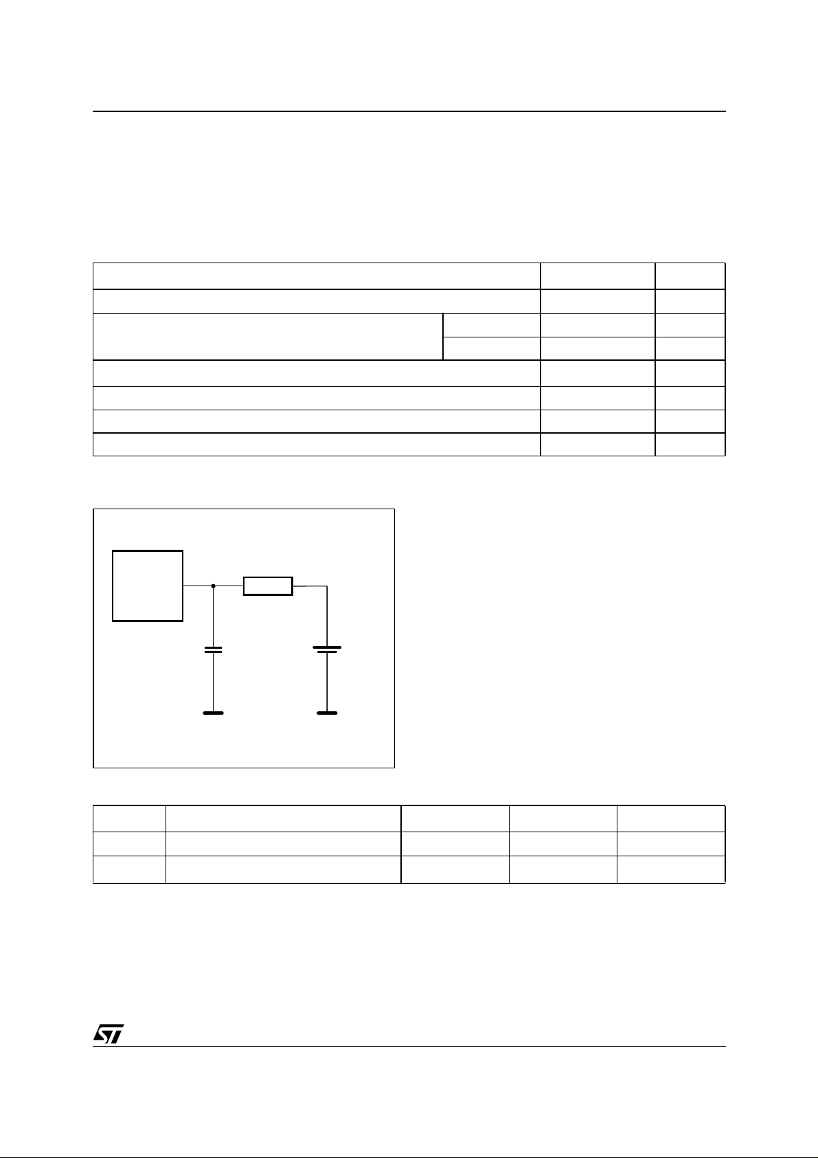
VCC Noise And Negative Going Transients
I
transients, including those produced by output
CC
switching, can produce voltage fluctuations, resulting in spikes on the V
bus. These transients
CC
can be reduced if capacitors are used to store energy which stabilizes the V
bus. The energy
CC
stored in the bypass capacitors will be released as
low going spikes are generated or energy will be
absorbed when overshoots occur. A ceramic bypass capacitor value of 0.1µ F (see Figure 10) is
recommended in order to provide the needed filterin g.
In addition to transients that are caused by normal
SRAM operation, power cycling can generate negative voltage spikes on VCC that drive it to values
below V
by as much as one volt. These negative
SS
spikes can cause data corruption in the SRAM
while in battery backup mode. To protect from
these voltage spikes, ST recommends connecting
a schottky diode from V
nected to V
, anode to VSS). (Schottky diode
CC
CC
to V
(cathode con-
SS
1N5817 is recommended for through hole and
MBRS120T3 is recommended for surface mount).
Figure 10. Supply Voltage Protection
V
CC
V
CC
0.1µF DEVICE
V
SS
AI02169
12/16
Page 13

M48Z32V
PART NUMBERING
Table 11. Ordering Information Scheme
Example: M48Z 32V –35 MT 1 TR
Device Type
M48Z
Supply Voltage and Write Protect Voltage
32V = V
Speed
–35 = 35ns
Package
MT = 44-lead, Hatless SOIC
= 3.0 to 3.6V; V
CC
= 2.7 to 3.0V
PFD
Temperature Rang e
1 = 0 to 70°C
6 = –40 to 85°C
Shipping Method for SOIC
blank = Tubes
TR = Tape & Reel
For a list of available options (e.g., Speed, Package) or for further information on any aspect of this device,
please contact the ST Sales Office nearest to you.
13/16
Page 14

M48Z32V
PACKAGE MECHANICAL INFORMATION
Figure 11. SOH44 – 44-lead Plastic, Hatless, Small Package Outline
A2
A
Be
CP
D
N
E
H
1
SOH-C
Note: Drawing is not to scale.
Table 12. SOH44 – 44-lead Plastic, Hatless, Small Package Mechanical Data
Symbol
T yp Min Max Typ Min Max
A 3.05 0.120
mm inch
C
LA1 α
A1 0.05 0.36 0.002 0.014
A2 2.34 2.69 0.092 0.106
B 0.36 0.46 0.014 0.018
C 0.15 0.32 0.006 0.012
D 17.71 18.49 0.697 0.728
E 8.23 8.89 0.324 0.350
e 0.81 – – 0.032 – –
H 1 1.51 12.70 0.453 0.500
L 0.41 1.27 0.016 0.050
α 0° 8° 0° 8°
N44 44
CP 0.10 0.004
14/16
Page 15

REVISION HIST ORY
Table 13. Revision History
Date Rev. # Revision Details
October 2002 1.0 First Issue
11/07/02 1.1 Update Absolute Maximum Ratings, DC Characteristics (Table 2, 5)
M48Z32V
15/16
Page 16

M48Z32V
Information furnished is believed to be accurate and reliable. However, STMicroelectronics assumes no responsibility for the consequences
of use of such information nor for any infringement of patents or other rights of third parties which may result from its use. No license is granted
by implic ation or otherwise under any patent or patent ri ghts of STM i croelectr onics. Specifications menti oned in thi s publicati on are subject
to change without notice. This publication supersedes and replaces all information previously supplied. STMicroelectronics products are not
authorized for use as cri tical comp onents in lif e support devi ces or systems without express written approv al of STMicroel ectronics.
The ST log o i s registered trademark of STMicroelectronics
All other na m es are the property of their respective owners.
© 2002 STMicroelectronics - All Rights Reserved
Australi a - Brazil - Canada - Chin a - F i nl and - Franc e - Germany - H ong Kong - India - Israel - Ital y - Japan - M al aysia -
Malta - Mor occo - Singapore - Spain - S weden - Switzerland - United Kingdom - U.S. A.
STMicroelectronics GROUP OF COMPANIES
www.st.c om
16/16
 Loading...