

Page 1
AI01184
13
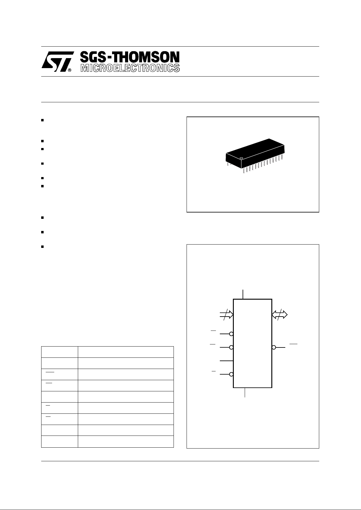
A0-A12
W
DQ0-DQ7
V
CC
M48Z09
M48Z19
G
E2
V
SS
8
E1 INT
Figure 1. Logic Diagram
M48Z09
M48Z19
CMOS 8K x 8 ZEROPOWER SRAM
INTEGRATED ULTRA LOW POWER SRAM,
POWE R-FAIL CONTROL CIRCUI T and
BA TTERY
UNLIMITED WRI TE CYCLE S
READ CYCLE TIME EQUALS WRITE CYCLE
TIME
AUTOMA TIC POWER-F AIL CHIP DESELECT and
WRITE PROTECTION
POWER-FAIL INTERRUP T
CHOICE of TWO WRITE PROTECT
VOLTAGES:
– M48Z09: 4. 5V ≤ V
PFD
≤ 4.75V
– M48Z19: 4. 2V ≤ V
PFD
≤ 4.5V
SELF CONTAI NED B ATTER Y in the C AP HAT
DIP PACKAGE
11 YEARS of DAT A RETENTION in the
ABSENCE of POWER
PIN and FUNCTIO N CO MPATIBLE with the
MK48Z09, 19 and JEDE C STANDARD 8K x 8
SRAMs
DESCRIPT IO N
The M48Z09,19 ZERO POWER
®
RAM is an 8K x 8
non-volatile static RAM which is pin and function
compatible with the MK48Z09, 19.
A special 28 pin 600mil DIP CAPHAT package
houses the M48Z09,19 silicon with a long life lithium button cell to form a highly integrated battery
backed-up memory solut ion.
A0-A12 Address Inputs
DQ0-DQ7 Data Inputs / Outputs
INT Power Fail Interrupt
E1 Chip Enable 1
E2 Chip Enable 2
G Output Enable
W Write Enable
V
CC
Supply Voltage
V
SS
Ground
Table 1. Signal Names
28
1
PCDIP28 (PC)
Battery CAPHAT
November 1994 1/13
Page 2
Symbol Parameter Value Unit
T
A
Ambient Operating Temperature 0 to 70
°C
T
STG
Storage Temperature (VCC Off) –40 to 85
°C
V
IO
Input or Output Voltages –0.3 to 7 V
V
CC
Supply Voltage –0.3 to 7 V
I
O
Output Current 20 mA
P
D
Power Dissipation 1 W
Note: Stresses greater than those listed under "Absolute Maximum Ratings" may cause permanent damage to the device. This is a stress
rating only and functional operation of the device at these or any other conditions above those indicated in the operational section of this
specification is not implied. Ex p osur e to the absolut e maximum rat ings conditi ons for extended periods of time may affect reliability.
CAUTION: Negative undershoots below –0.3 volts are not allowed on any pin while in the Battery Back-up mode.
Table 2. Absolut e Maxi mum Rat in gs
Mode V
CC
E1 E2 G W DQ0-DQ7 Power
Deselect
4.75V to 5.5V
or
4.5V to 5.5V
V
IH
X X X High Z Standby
Deselect X V
IL
X X High Z Standby
Write V
IL
V
IH
XVILD
IN
Active
Read V
IL
V
IH
V
IL
V
IH
D
OUT
Active
Read V
IL
V
IH
V
IH
V
IH
High Z Active
Deselect V
SO
to V
PFD
(min) X X X X High Z CMOS Standby
Deselect
≤ V
SO
X X X X High Z Battery Back-up Mode
Note: X = VIH or V
IL
Table 3. Operating Modes
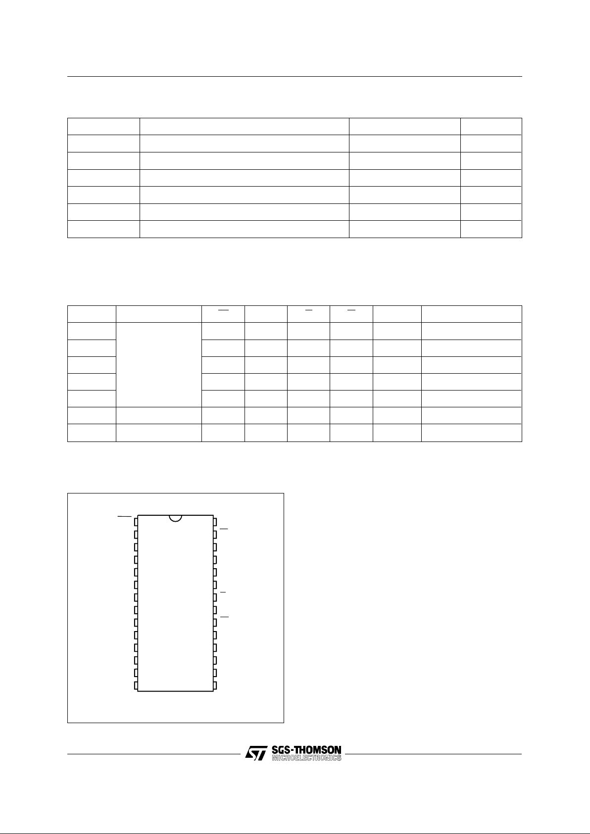
A1
A0
DQ0
A7
A4
A3
A2
A6
A5
E2
A10
A8
A9
DQ7
W
A11
G
E1
DQ5DQ1
DQ2
DQ3V
SS
DQ4
DQ6
A12
INT V
CC
AI01185
M48Z09
M49Z19
8
1
2
3
4
5
6
7
9
10
11
12
13
14
16
15
28
27
26
25
24
23
22
21
20
19
18
17
Figure 2A. DIP Pin Connections
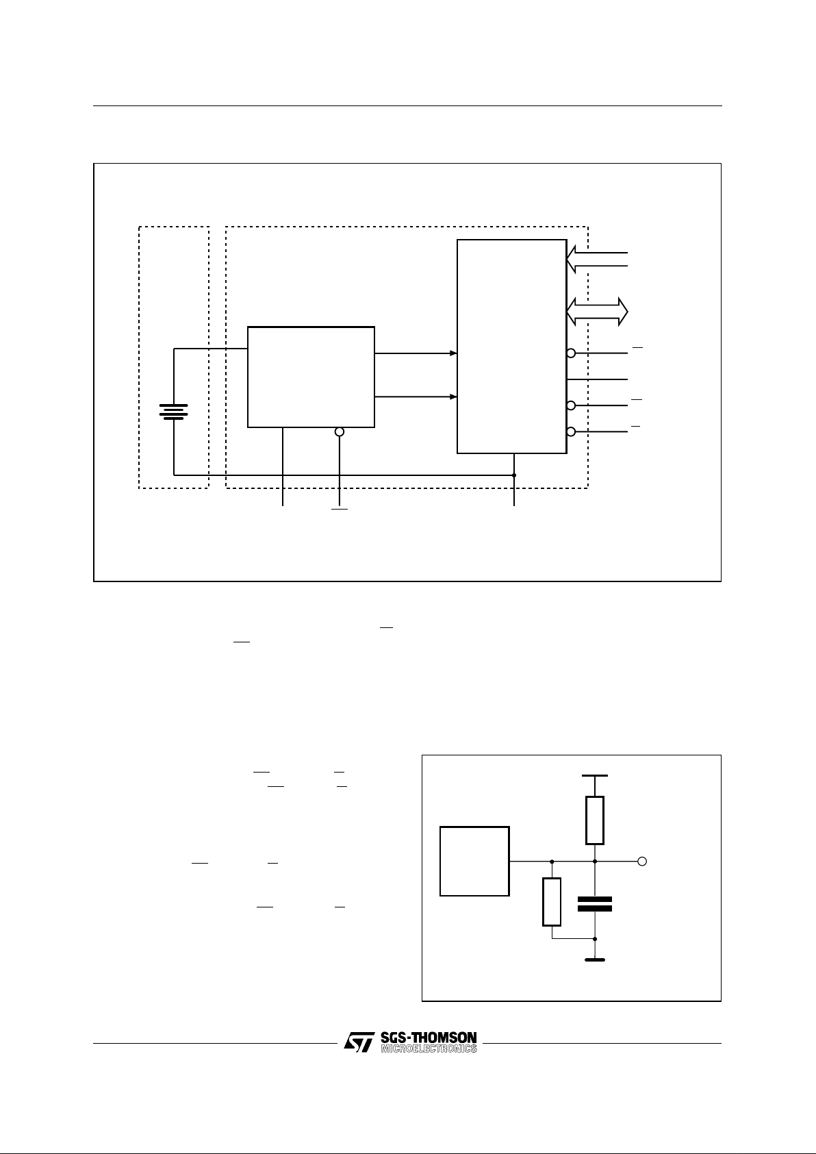
The M48Z09,19 button cell has sufficient capacity
and storage life to maintain data for an accumulated time period of at least 1 1 years in the absence
of power over the operating temp erature range.
The M48Z09,19 is a non-volatile pin and function
equivalent to any JEDEC standard 8K x 8 SRAM.
It also easily fits into many ROM, EPROM, and
EEPROM sockets, providing the non-volatility of
PROMs without any requirement for special write
timing or limitations on the number of writes that
can be performed.
The M48Z09,19 also has it s own Power-f ail Detect
circuit. The control circ uitry constantly monitor s the
single 5V supply for an out of tolerance condition.
When V
CC
is out of tolerance, the circuit write
protects the SRAM, providing a high degree of data
security in the midst of unpredict able system operation brought on by low V
CC
. As VCC falls below
approximately 3V, the cont rol circuitry connects the
battery which maintains data and clock operation
until valid power returns.
DESCRIPTI ON (cont ’d )
2/13
M48Z09, M4 8Z19
Page 3
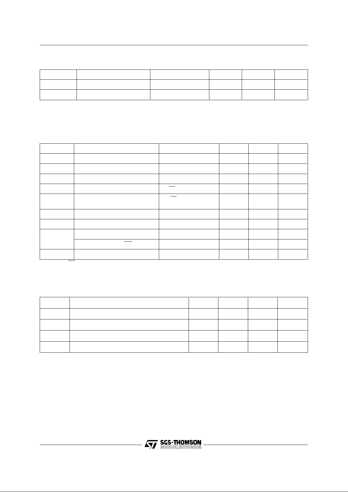
AI01398
5V
OUT
CL = 100pF or 30pF
CL includes JIG capacitance
1.8kΩ
DEVICE
UNDER
TEST
1kΩ
Figure 4. AC Test ing L o ad Circuit
Input Rise and Fall Times
≤ 5ns
Input Pulse Voltages 0 to 3V
Input and Output Timing Ref. Voltages 1.5V
AC MEASUREMEN T CONDI TIONS
Note that Output Hi-Z is defined as the point where data
is no longer driven.
AI01397
LITHIUM
CELL
V
PFD
V
CC
V
SS
VOLTAGE SENSE
AND
SWITCHING
CIRCUITRY
8K x 8
SRAM ARRAY
A0-A12
DQ0-DQ7
E1
W
G
POWER
E2
INT
Figure 3. Block Diagram
READ MODE
The M48Z09,19 is in the Read Mode whenever W
(Write Enable) is high,
E1 (Chip Enable 1) is low,
and E2 (Chip Enable 2) is high. The device architecture all ows ripple- through access of data from
eight of 65,536 locations in the static storage array .
Thus, the unique address specified by the 13 Address Inputs defines which one of the 8,192 bytes
of data is to be accessed. Valid data will be available at the Data I/O pins within t
AVQV
(Address
Access Time) after the last address input signal is
stable, providing that the
E1, E2, and G access
times are also satisf ied. If the
E1, E2 and G access
times are not met, valid data will be available after
the latter of the Chip Enable Acces s T im es (t
E1LQV
or t
E2HQV
) or Output Enable Access Time (t
GLQV
).
The state of the eight three-state Data I/O signals
is controlled by
E1, E2 and G. If the o utputs are
activated bef ore t
AVQV
, the data lines will be driven
to an indeterminate state unt il t
A VQV
. If the A ddress
Inputs are changed while
E1, E2 and G remain
active, output data will remain valid for t
AXQX
(Output Data Hold Time) but will go indeterminate until
the next A ddress A ccess.
3/13
M48Z09, M48Z19
Page 4
Symbol Parameter Test Condition Min Max Unit
I
LI
Input Leakage Current
0V ≤ V
IN
≤ V
CC
±1 µA
I
LO
Output Leakage Current
0V ≤ V
OUT
≤ V
CC
±5 µA
I
CC
Supply Current Outputs open 80 mA
I
CC1
Supply Current (Standby) TTL E1 = VIH, E2 = V
IL
3mA
I
CC2
Supply Current (Standby) CMOS
E1 = VCC – 0.2V,
E2 = V
SS
+ 0.2V
3mA
V
IL
Input Low Voltage –0.3 0.8 V
V
IH
Input High Voltage 2.2 VCC + 0.3 V
V
OL
Output Low Voltage IOL = 2.1mA 0.4 V
Output Low Voltage (
INT)
(1)
IOL = 0.5mA 0.4 V
V
OH
Output High Voltage IOH = –1mA 2.4 V
Note: 1. The INT pin is Open Drain.
Table 5. DC Characteristics (TA = 0 to 70°C; VCC = 4.75V to 5.5V or 4.5V to 5.5V)
Symbol Parameter Test Condition Min Max Unit
C
IN
Input Capacitance VIN = 0V 10 pF
C
IO
(2)
Input / Output Capacitance V
OUT
= 0V 10 pF
Notes: 1. Effecti ve capacita nce calculated from th e equation C = I∆t/∆V with ∆V = 3V and power supply at 5V.
2. Outputs deselected
Table 4. Capacitance
(1)
(TA = 25 °C)
Symbol Parameter Min Typ Max Unit
V
PFD
Power-fail Deselect Voltage (M48Z09) 4.5 4.6 4.75 V
V
PFD
Power-fail Deselect Voltage (M48Z19) 4.2 4.3 4.5 V
V
SO
Battery Back-up Switchover Voltage 3.0 V
t
DR
Expected Data Retention Time 11 YEARS
Note: 1. All voltages referenced to VSS.
Table 6. Power Down/Up Trip Points DC Characteristics
(1)
(TA = 0 to 70°C)
4/13
M48Z09, M4 8Z19
Page 5

Symbol Parameter Min Max Unit
t
PD
E1 or W at VIH or E2 at VIL before Power Down 0
µs
t
F
(1)
V
PFD
(max) to V
PFD
(min) VCC Fall Time 300
µs
t
FB
(2)
V
PFD
(min) to VSO VCC Fall Time 10
µs
t
R
V
PFD
(min) to V
PFD
(max) VCC Rise Time 0
µs
t
RB
VSO to V
PFD
(min) VCC Rise Time 1
µs
t
REC
E1 or W at VIH or E2 at VIL after Power Up 1 ms
t
PFX
INT Low to Auto Deselect 10 40
µs
t
PFH
(3)
V
PFD
(max) to INT High 120
µs
Notes:1.V
PFD
(max) to V
PFD
(min) fall time of less than tF may result in deselection/write protect ion not occurring until 200 µs after
V
CC
passes V
PFD
(min).
2. V
PFD
(min) to VSO fall time of less than tFB may cause corruption of RAM data.
3.
INT may go high anytime after VCC exceeds V
PFD
(min) and is guaranteed to go high t
PFH
after VCC exceeds V
PFD
(max).
Table 7. Power Down/Up Mode AC Characteristics (TA = 0 to 70°C)
AI00566
V
CC
INPUTS
INT
(PER CONTROL INPUT)
OUTPUTS
DON'T CARE
HIGH-Z
tF
tFB
tPFX
tR
tPFH
tREC
tPD tRB
tDR
VALID VALID
NOTE
(PER CONTROL INPUT)
RECOGNIZEDRECOGNIZED
V
PFD
(max)
V
PFD
(min)
VSO
Figure 5. Power Down/Up Mode AC Waveforms
Note: Inputs may or may not be recognized at this time. Caution should be taken to keep E1 high or E2 low as VCC rises past V
PFD
(min).
Some systems may performs inadvertent write cycles after V
CC
rises above V
PFD
(min) but before normal system operations begins. Even
though a power on reset is being applied to the processor a reset condition may not occur until after th e system clock is running.
5/13
M48Z09, M48Z19
Page 6

Symbol Parameter
M48Z09 / 19
Unit
-100
Min Max
t
AVAV
Read Cycle Time 100 ns
t
AVQV
(1)
Address Valid to Output Valid 100 ns
t
E1LQV
(1)
Chip Enable 1 Low to Output Valid 100 ns
t
E2HQV
(1)
Chip Enable 2 High to Output Valid 100 ns
t
GLQV
(1)
Output Enable Low to Output Valid 50 ns
t
E1LQX
(2)
Chip Enable 1 Low to Output Transition 10 ns
t
E2HQX
(2)
Chip Enable 2 High to Output Transition 10 ns
t
GLQX
(2)
Output Enable Low to Output Transition 5 ns
t
E1HQZ
(2)
Chip Enable 1 High to Output Hi-Z 50 ns
t
E2LQZ
(2)
Chip Enable 2 Low to Output Hi-Z 50 ns
t
GHQZ
(2)
Output Enable High to Output Hi-Z 40 ns
t
AXQX
(1)
Address Transition to Output Transition 5 ns
Notes: 1. CL= 100pF (see Figure 4).
2. C
L
= 30pF (see Figure 4)
T able 8. Read Mode AC Characteristics (TA = 0 to 70°C; VCC = 4.75V to 5.5V or 4. 5V to 5.5V)
AI00962
tAVAV
tAVQV tAXQX
tE1LQV
tE1LQX
tE1HQZ
tGLQV
tGLQX
tGHQZ
VALID
A0-A12
E1
G
DQ0-DQ7
tE2HQV
tE2HQX
VALID
tE2LQZ
E2
Figure 6. Read Mode AC Waveforms
6/13
M48Z09, M4 8Z19
Page 7

Symbol Parameter
M48Z09 / 19
Unit
-100
Min Max
t
AVAV
Write Cycle Time 100 ns
t
AVWL
Address Valid to Write Enable Low 0 ns
t
AVE1L
Address Valid to Chip Enable 1 Low 0 ns
t
AVE2H
Address Valid to Chip Enable 2 High 0 ns
t
WLWH
Write Enable Pulse Width 80 ns
t
E1LE1H
Chip Enable 1 Low to Chip Enable 1 High 80 ns
t
E2HE2L
Chip Enable 2 High to Chip Enable 2 Low 80 ns
t
WHAX
Write Enable High to Address Transition 10 ns
t
E1HAX
Chip Enable 1 High to Address Transition 10 ns
t
E2LAX
Chip Enable 2 Low to Address Transition 10 ns
t
DVWH
Input Valid to Write Enable High 50 ns
t
DVE1H
Input Valid to Chip Enable 1 High 50 ns
t
DVE2L
Input Valid to Chip Enable 2 Low 50 ns
t
WHDX
Write Enable High to Input Transition 5 ns
t
E1HDX
Chip Enable 1 High to Input Transition 5 ns
t
E2LDX
Chip Enable 2 Low to Input Transition 5 ns
t
WLQZ
(1, 2)
Write Enable Low to Output Hi-Z 50 ns
t
AVWH
Address Valid to Write Enable High 80 ns
t
AVE1H
Address Valid to Chip Enable 1 High 80 ns
t
AVE2L
Address Valid to Chip Enable 2 Low 80 ns
t
WHQX
(1, 2)
Write Enable High to Output Transition 10 ns
Notes: 1. CL= 30pF (see Figure 4).
2. If
E1 goes low or E2 high simultaneously with W going low, the out puts remain in the high impedance state.
Table 9. Write Mode AC Ch aracteri stic s (TA = 0 to 70°C; VCC = 4.75V to 5.5V or 4.5V to 5.5V)
7/13
M48Z09, M48Z19
Page 8

AI00963
tAVAV
tWHAX
tDVWH
DATA INPUT
A0-A12
E1
W
DQ0-DQ7
VALID
E2
tAVWH
tAVE1L
tAVE2H
tWLWH
tAVWL
tWLQZ
tWHDX
tWHQX
Figure 7. Write E nab le C ontro l led, W rit e AC Waveforms
AI00964B
tAVAV
tE1HAX
tDVE1H
tDVE2L
A0-A12
E1
W
DQ0-DQ7
VALID
E2
tAVE1H
tAVE1L
tAVWL
tAVE2L
tE1LE1H
tE2LAX
tAVE2H tE2HE2L
tE1HDX
tE2LDX
DATA INPUT
Figure 8. Chip En ab le Con t roll ed, W ri te AC Waveforms
8/13
M48Z09, M4 8Z19
Page 9

WRITE MODE
The M48Z09,19 is in the Write Mode wh enever
W,
E1, and E2 are active. The start of a write is referenced from the latt er occurring falling edge of
W or
E1, or the rising edge of E2. A write is terminated
by the earlier rising edge of
W or E1, or the falling
edge of E2. The addresses must be held valid
throughout the cycle .
E1 or W must return high or
E2 low for minimum of t
E1HAX
or t
E2LAX
from Chip
Enable or t
WHAX
from Write Enable prior to the
initiation of another read or write cycle. Data-in
must be valid t
DVWH
prior to the end of write and
remain valid for t
WHDX
afterward. G sho uld be kept
high during write cycles to avoid bus contention;
although, if the output bus has been activated by a
low on
E1 and G and a high on E2, a low on W will
disable the outputs t
WLQZ
after W falls.
DATA RETENTION MODE
With va lid VCC applied, the M48Z09,19 operates as
a conventional BYTEWIDE static RAM. Should
the supply voltage decay, the RAM will automatically power-fail deselect, write protecting itself
when V
CC
falls within the V
PFD
(max), V
PFD
(min)
window. All outputs become high impedance, and
all inputs are treated as "don’t care."
Note: A power failure during a write cycle may
corrupt data at the currently addressed location, but
does not jeopardize the rest of the RA M’s content.
At voltages below V
PFD
(min), the user can be assured the memory will be in a write protected stat e,
provided the V
CC
fall time is not less than tF. The
M48Z09,19 may respond to transient noise spikes
on V
CC
that reach into the deselect window during
the time the device is sampling V
CC
. Therefore,
decoupling of the power supply lines is recommended.
When V
CC
drops below VSO, the control circuit
switches power to the internal battery which preserves data and powers the clock. The internal
button cell will maintain data in the M48Z09,19 for
an accumulated period of at least 10 years when
V
CC
is less than VSO. As system power returns and
V
CC
rises above VSO, the battery is disconnected,
and the power supply is switched to external V
CC
.
Write protection continues until V
CC
reaches
V
PFD
(min). E1 should be kept high o r E2 low as
V
CC
rises past V
PFD
(min) to prevent inadvertent
write cycles prior t o processor stabilization. Normal
RAM operation can resume t
REC
after VCC exceeds
V
PFD
(max).
POWER F AI L I NTERRU PT PIN
The M48Z09,19 continuously monitor s V
CC
. When
V
CC
falls to the power-fail detect trip point, an
interrupt is immediately generated. An internal
clock provides a delay of between 10µs and 40µs
before automatically deselecting the M48Z09,19.
The
INT pin is an open drain output and requires
an external pull up resistor, even if the interrupt
output function is not being used.
SYSTEM BATTERY LIFE
The useful life of the battery in the M48Z09,19 is
expected to ultimately come to an end for one of
two reasons: either because it has been discharged
while providing current to the RAM in the battery
back-up mode, or because the effects of aging
render the cell useless before it can actually be
completely discharged. The two effect s are virtually
unrelated allowing discharge, or Capacity Consumption, and the eff ects of aging, or St orage Life,
to be treated as two independent but simultaneous
mechanisms. The earlier occurring failure mecha nism defines the battery system life of the
M48Z09,19.
Cell Storag e L i f e
Storage life is primarily a function of temperature.
Figure 9 illustrates the approximate storage life of
the M48Z09,19 battery over temperature. The results in Figure 9 are derived from temperature
accelerated life test studies performed at SGSTHOMSON. For the purpose of the testing, a cell
failure is defined as the inability of a cell stabilized
at 25°C to produce a 2.4V closed circuit voltage
across a 250 kΩ load resistor. The two lines, t
1%
and t
50%
, represent different failure rate distributions for the cell’ s storage life. At 7 0°C, for example,
the t
1%
line indicates that an M 48Z09,19 has a 1%
chance of having a battery failure 28 years into its
life while the t
50%
shows the part has a 50% chance
of failure at the 50 year mark. The t
1%
line represents the practical onset of wear out and can be
considered the worst case S torage Life f or the cell.
The t
50%
can be considered the normal or average
life.
9/13
M48Z09, M48Z19
Page 10

Calcul ati ng Sto rage L if e
The following formula can be used to predict storage life:
1
{[(TA1/TT)/SL1]+[(TA2/TT)/SL2]+...+[(TAN/TT)/SLN]}
where,
– TA1, TA2, T A N = time at ambient t emperat ure
1, 2, etc.
– TT = t otal time = TA1+TA2+...+T AN
– SL1, SL2, SLN = storage life at temperat ure 1,
2, etc.
For example an M48Z09,19 is exposed to tempera-
tures of 55°C or less for 8322 hrs/yr, and temperatures greater than 60°C but less than 70°C for the
remaining 438 hrs/yr . Reading predicted t
1%
values
from Figure 9,
– SL1 ≅ 200 yrs, SL2 = 28 yrs
– TT = 8760 hrs/ yr
– TA1 = 8322 hrs/yr , TA2 = 438 hrs/yr
Predicted storage lif e ≥
1
{[(8322/8760)/200]+[(431/8760)/28]}
or 154 years.
As can be seen from these calculations and the
results, the expected life time of the M48Z09, 19
should exceed most system requirements.
Estimated S ystem L ife
Since either storage life or capacity consumption
can end the battery’s life, the sy stem life is marke d
by which ever occurs fir st.
Reference for System Life
Each M48Z09,19 is marked with a nine digit manufacturing date code in the form of H99XXYYZZ. For
example, H995B9431 is:
H = fabricated in Carrollton, TX
9 = assembled in Muar , Ma laysia,
9 = tested in Muar , Malay sia,
5B = lot designator,
9431 = assembled in the year 1994, work week 31.
AI01399
20 30 40 50 60 70 80 90
1
2
3
4
5
8
6
TEMPERATURE (Degrees Celsius)
10
20
30
40
50
YEARS
t50% (AVERAGE)
t1%
Figure 9. Predicted Battery St orag e Lif e versus Temperature
10/13
M48Z09, M4 8Z19
Page 11

ORDERING INFORMATION SCHEME
Supply Voltage and Write
Protect Voltage
09 VCC = 4.75V to 5.5V
V
PFD
= 4.5V to 4.75V
19 V
CC
= 4.5V to 5.5V
V
PFD
= 4.2V to 4.5V
Speed
-100 100ns
Package
PC PCDIP28
Temp. Range
1
0 to 70 °C
Example: M48Z09 -100 PC 1
For a list of available options (Supply Voltage, Speed, Package, etc...) refer to the current Memory
Shortform cat alogue.
For further in formation on any aspect of this device, please contact the SGS-THOMSON Sales Office
nearest to you.
11/13
M48Z09, M48Z19
Page 12

PCDIP
A2
A1AL
B1 B e1
D
E
N
1
C
eA
e3
Symb
mm inches
Typ Min Max Typ Min Max
A 8.89 9.65 0.350 0.380
A1 0.38 0.76 0.015 0.030
A2 8.38 8.89 0.330 0.350
B 0.38 0.53 0.015 0.021
B1 1.14 1.78 0.045 0.070
C 0.20 0.31 0.008 0.012
D 39.37 39.88 1.550 1.570
E 17.83 18.34 0.702 0.722
e1 2.29 2.79 0.090 0.110
e3 29.72 36.32 1.170 1.430
eA 15.24 16.00 0.600 0.630
L 3.05 3.81 0.120 0.150
N28 28
PCDIP28
Drawing is not to scale
PCDIP28 - 28 pin Plastic DIP, battery CAPHAT
12/13
M48Z09, M4 8Z19
Page 13

Information furnished is believed to be accurate and reliable. How ever, SGS-THOMSON Microelectronics a ssumes no responsibility for the
consequences of use of such information nor for any infringement of patents or other rights of third parties which may result from its use. No
license is granted by implication or otherwise under any patent or patent rights of SGS-THOMSON Microelectronics. Specifications mentioned
in this publication are subject to change without notice. This publication supersedes and replaces all information previously supplied.
SGS-THOMSON Microelectronics products are not authorized for use as critical components in life support devices or systems with out express
written approval of SGS-THOMSON Microelectronics.
© 1994 SGS-THOMSON Microelectronics - All Rights Reserved
® ZEROPOWER is a registered trademark of SGS-THOMSON Microelectronics
CAPHAT and BYTEWIDE are trademarks of SGS-THOMSON Microelectronics
SGS-THOMSON Microelectronics GROUP OF COMPANIES
Australia - Brazil - China - France - Germany - Hong Kong - Italy - Japan - Korea - Malaysia - Malta - Morocco - The Netherlands -
Singapore - Spain - Sweden - Switzerland - Taiwan - Thailand - United Kingdom - U.S.A.
13/13
M48Z09, M48Z19
 Loading...