

Page 1
5.0 or 3.3V, 64 Kbit (8 Kbit x8) TIMEKEEPER® SRAM
FEAT URES SUM MARY
■ INTEGRATED ULTRA LOW POWER SRAM,
REAL TIME CLOCK, POWER-FAIL
CONTROL CIRCUIT, AND BATTERY
■ FREQUENCY TEST OUTPUT FOR REAL
TIME CLOCK SOFTWARE CALIBRATION
■ AUTOMATIC POWER-FAIL CHIP
DESELECT AND WRITE PROTECT ION
■ WRITE PROTECT VOLTAGES
= Power-fail Deselect Voltage):
(V
PFD
– M48T59: V
4.5V ≤ V
– M48T59Y: V
4.2V ≤ V
– M48T59V*: V
2.7V ≤ V
■ SELF-CONTAINED BATTERY AND
CRYSTAL IN THE CAPHAT™ DIP
PACKAGE
■ PACKAGING INCLUDES A 28-LEAD SOIC
AND SNAPHAT
separately)
■ SOIC PACKAGE PROVIDES DIRECT
CONNECTION FOR A SNAPHAT TOP
WHICH CONTAINS THE BATTERY AND
CRYSTAL
■ MICROPROCESSOR POWER-ON RESET
(Valid even during battery back-up mode)
■ PROGRAMMABLE ALAR M OUTPUT
ACTIVE IN THE BATTERY BACK-UP MODE
■ BATTERY LOW FLAG
= 4.75 to 5.5V
CC
≤ 4.75V
PFD
= 4.5 to 5.5V
CC
≤ 4.5V
PFD
= 3.0 to 3.6V
CC
≤ 3.0V
PFD
®
TOP (to be ordered
M48T59
M48T59Y, M48 T5 9V *
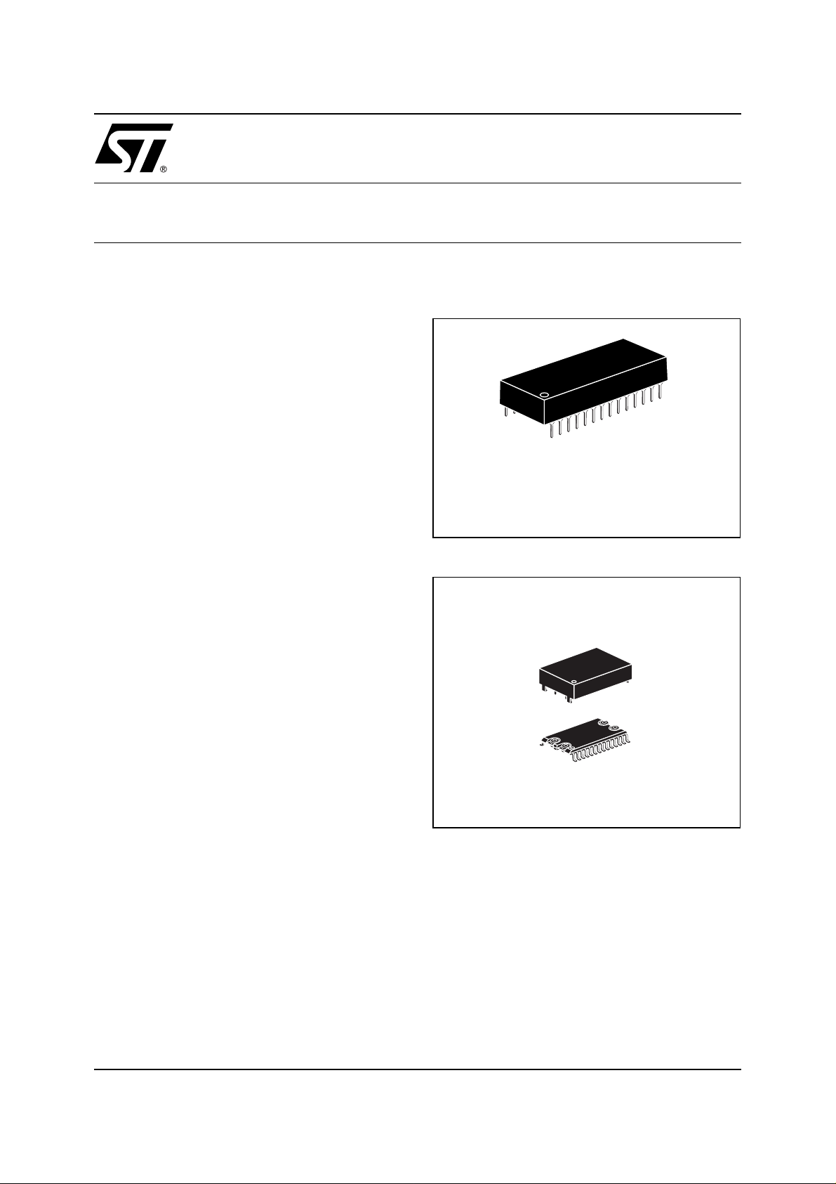
Figure 1. 28-pin PCDIP, CAPHAT™ Package
28
1
PCDIP28 (PC)
Battery/Crystal
CAPHAT
Figure 2. 28-pi n S O I C Package
SNAPHAT (SH)
Battery/Crystal
28
1
SOH28 (MH)
* Contact local ST sales office for availability of 3.3V version.
1/29November 2004
Page 2

M48T59, M48T59Y, M48T59V*
TABLE OF CONTENTS
FEATURES SUMMARY . . . . . . . . . . . . . . . . . . . . . . . . . . . . . . . . . . . . . . . . . . . . . . . . . . . . . . . . . . . . . 1
Figure 1. 28-pin PCDIP, CAPHAT™ Package . . . . . . . . . . . . . . . . . . . . . . . . . . . . . . . . . . . . . . . . . 1
Figure 2. 28-pin SOIC Package . . . . . . . . . . . . . . . . . . . . . . . . . . . . . . . . . . . . . . . . . . . . . . . . . . . . 1
SUMMARY DESCRIPTION. . . . . . . . . . . . . . . . . . . . . . . . . . . . . . . . . . . . . . . . . . . . . . . . . . . . . . . . . . . 4
Figure 3. Logic Diagram . . . . . . . . . . . . . . . . . . . . . . . . . . . . . . . . . . . . . . . . . . . . . . . . . . . . . . . . . . 4
Table 1. Signal Names . . . . . . . . . . . . . . . . . . . . . . . . . . . . . . . . . . . . . . . . . . . . . . . . . . . . . . . . . . 4
Figure 4. 28-pin SOIC Connections . . . . . . . . . . . . . . . . . . . . . . . . . . . . . . . . . . . . . . . . . . . . . . . . . 5
Figure 5. PCDIP28 CAPHAT Connections . . . . . . . . . . . . . . . . . . . . . . . . . . . . . . . . . . . . . . . . . . . . 5
Figure 6. Block Diagram . . . . . . . . . . . . . . . . . . . . . . . . . . . . . . . . . . . . . . . . . . . . . . . . . . . . . . . . . . 5
OPERATION MODES . . . . . . . . . . . . . . . . . . . . . . . . . . . . . . . . . . . . . . . . . . . . . . . . . . . . . . . . . . . . . . . 6
Table 2. Operating Modes. . . . . . . . . . . . . . . . . . . . . . . . . . . . . . . . . . . . . . . . . . . . . . . . . . . . . . . . 6
READ Mode . . . . . . . . . . . . . . . . . . . . . . . . . . . . . . . . . . . . . . . . . . . . . . . . . . . . . . . . . . . . . . . . . . . 7
Figure 7. READ Mode AC Waveforms . . . . . . . . . . . . . . . . . . . . . . . . . . . . . . . . . . . . . . . . . . . . . . . 7
Table 3. RE A D Mode AC Charac teristics . . . . . . . . . . . . . . . . . . . . . . . . . . . . . . . . . . . . . . . . . . . .7
WRITE Mode. . . . . . . . . . . . . . . . . . . . . . . . . . . . . . . . . . . . . . . . . . . . . . . . . . . . . . . . . . . . . . . . . . . 8
Figure 8. WRITE Enable Controlled, WRITE Mode AC Waveforms. . . . . . . . . . . . . . . . . . . . . . . . .8
Figure 9. Chip Enable Controlled, WRITE Mode AC Waveforms. . . . . . . . . . . . . . . . . . . . . . . . . . . 8
Table 4. WRITE Mode AC Characteristics . . . . . . . . . . . . . . . . . . . . . . . . . . . . . . . . . . . . . . . . . . . 9
Data Retention Mode. . . . . . . . . . . . . . . . . . . . . . . . . . . . . . . . . . . . . . . . . . . . . . . . . . . . . . . . . . . 1 0
CLOCK OPERATIONS . . . . . . . . . . . . . . . . . . . . . . . . . . . . . . . . . . . . . . . . . . . . . . . . . . . . . . . . . . . . . 11
Reading the Clock. . . . . . . . . . . . . . . . . . . . . . . . . . . . . . . . . . . . . . . . . . . . . . . . . . . . . . . . . . . . . 11
Setting the Clock. . . . . . . . . . . . . . . . . . . . . . . . . . . . . . . . . . . . . . . . . . . . . . . . . . . . . . . . . . . . . . 11
Stopping and Starting the Oscillator. . . . . . . . . . . . . . . . . . . . . . . . . . . . . . . . . . . . . . . . . . . . . . 11
Table 5. Register Map . . . . . . . . . . . . . . . . . . . . . . . . . . . . . . . . . . . . . . . . . . . . . . . . . . . . . . . . . . 12
Calibrating the Clock. . . . . . . . . . . . . . . . . . . . . . . . . . . . . . . . . . . . . . . . . . . . . . . . . . . . . . . . . . . 13
Figure 10.Crystal Accuracy Across Temperature . . . . . . . . . . . . . . . . . . . . . . . . . . . . . . . . . . . . . . 14
Figure 11.Clock Calibration. . . . . . . . . . . . . . . . . . . . . . . . . . . . . . . . . . . . . . . . . . . . . . . . . . . . . . . 14
Setting the Alarm Clock . . . . . . . . . . . . . . . . . . . . . . . . . . . . . . . . . . . . . . . . . . . . . . . . . . . . . . . . 15
Figure 12.Alarm Interrupt Reset Waveform. . . . . . . . . . . . . . . . . . . . . . . . . . . . . . . . . . . . . . . . . . .15
Table 6. A larm Repeat Mode. . . . . . . . . . . . . . . . . . . . . . . . . . . . . . . . . . . . . . . . . . . . . . . . . . . . . 15
Figure 13.Back-up Mode Alarm Waveforms . . . . . . . . . . . . . . . . . . . . . . . . . . . . . . . . . . . . . . . . . . 16
Watchdog Timer . . . . . . . . . . . . . . . . . . . . . . . . . . . . . . . . . . . . . . . . . . . . . . . . . . . . . . . . . . . . . . 17
Power-on Reset . . . . . . . . . . . . . . . . . . . . . . . . . . . . . . . . . . . . . . . . . . . . . . . . . . . . . . . . . . . . . . . 17
Programmable Interrupts . . . . . . . . . . . . . . . . . . . . . . . . . . . . . . . . . . . . . . . . . . . . . . . . . . . . . . . 17
Battery Low Flag . . . . . . . . . . . . . . . . . . . . . . . . . . . . . . . . . . . . . . . . . . . . . . . . . . . . . . . . . . . . . . 17
Century Bit. . . . . . . . . . . . . . . . . . . . . . . . . . . . . . . . . . . . . . . . . . . . . . . . . . . . . . . . . . . . . . . . . . . 18
Initial Power-on Defaults. . . . . . . . . . . . . . . . . . . . . . . . . . . . . . . . . . . . . . . . . . . . . . . . . . . . . . . . 18
Table 7. Default Values . . . . . . . . . . . . . . . . . . . . . . . . . . . . . . . . . . . . . . . . . . . . . . . . . . . . . . . . . 18
V
Noise And Negative Going Transients. . . . . . . . . . . . . . . . . . . . . . . . . . . . . . . . . . . . . . . . . 18
CC
Figure 14.Supply Voltage Protection. . . . . . . . . . . . . . . . . . . . . . . . . . . . . . . . . . . . . . . . . . . . . . . . 18
2/29
Page 3

M48T59, M48T59Y, M48T59V*
MAXIMUM RATING. . . . . . . . . . . . . . . . . . . . . . . . . . . . . . . . . . . . . . . . . . . . . . . . . . . . . . . . . . . . . . . . 19
Table 8. Absolute Maximum Ratings. . . . . . . . . . . . . . . . . . . . . . . . . . . . . . . . . . . . . . . . . . . . . . . 19
DC AND AC PARAMETERS. . . . . . . . . . . . . . . . . . . . . . . . . . . . . . . . . . . . . . . . . . . . . . . . . . . . . . . . . 20
Table 9. Operating and AC Measurement Conditions. . . . . . . . . . . . . . . . . . . . . . . . . . . . . . . . . . 20
Figure 15.AC Measurement Load Circuit . . . . . . . . . . . . . . . . . . . . . . . . . . . . . . . . . . . . . . . . . . . . 20
Table 10.Capacitance. . . . . . . . . . . . . . . . . . . . . . . . . . . . . . . . . . . . . . . . . . . . . . . . . . . . . . . . . . . 20
Table 11.DC Characteristics. . . . . . . . . . . . . . . . . . . . . . . . . . . . . . . . . . . . . . . . . . . . . . . . . . . . . . 21
Figure 16.Power Down/Up Mode AC Waveforms. . . . . . . . . . . . . . . . . . . . . . . . . . . . . . . . . . . . . . 22
Table 12.Power Down/Up AC Characteristics . . . . . . . . . . . . . . . . . . . . . . . . . . . . . . . . . . . . . . . . 22
Table 13.Power Down/Up Trip Points DC Characteristics . . . . . . . . . . . . . . . . . . . . . . . . . . . . . . . 22
PACKAGE MECHANICAL INFORMATION . . . . . . . . . . . . . . . . . . . . . . . . . . . . . . . . . . . . . . . . . . . . . 23
Figure 17.PCDIP28 – 28-pin Plastic DIP, battery CAPHAT, Package Outline . . . . . . . . . . . . . . . . 23
Table 14. PCDIP28 – 28-pin Plastic DIP, battery CAPHAT, Package Mechanical Data. . . . . . . . . 23
Figure 18.SOH28 – 28-lead Plastic Small Outline, battery SNAPHAT, Package Outline . . . . . . . . 24
Table 15. SOH28 – 28-lead Plastic Small Outline, battery SNAPHAT, Pack. Mech. Data . . . . . . . 24
Figure 19.SH – 4-pin SNAPHAT Housing for 48mAh Battery & Crystal, Package Outline . . . . . . . 25
Table 16. SH – 4-pin SNAPHAT Housing for 48mAh Battery & Crystal, Package Mech. Data. . . . 25
Figure 20.SH – 4-pin SNAPHAT Housing for 120mAh Battery & Crystal, Package Outline . . . . . . 26
Table 17. SH – 4-pin SNAPHAT Housing for 120mAh Battery & Crystal, Package Mech. Data. . . 26
PART NUMBERING . . . . . . . . . . . . . . . . . . . . . . . . . . . . . . . . . . . . . . . . . . . . . . . . . . . . . . . . . . . . . . . 27
Table 18.Ordering Information Scheme . . . . . . . . . . . . . . . . . . . . . . . . . . . . . . . . . . . . . . . . . . . . . 27
Table 19.SNAPHAT Battery Table . . . . . . . . . . . . . . . . . . . . . . . . . . . . . . . . . . . . . . . . . . . . . . . . .27
REVISION HISTORY. . . . . . . . . . . . . . . . . . . . . . . . . . . . . . . . . . . . . . . . . . . . . . . . . . . . . . . . . . . . . . . 28
Table 20.Document Revision History. . . . . . . . . . . . . . . . . . . . . . . . . . . . . . . . . . . . . . . . . . . . . . . 28
3/29
Page 4

M48T59, M48T59Y, M48T59V*
SUMMARY DESCRIPTIO N
The M48T59/Y/V TIMEKEEPER® RAM is an
8 Kb x8 non-volatile static RAM and real time
clock. The monolithic chip is available in two special packages to provid e a highly integrated battery backed-up memory and real time clock
solution.
The M48T59/Y/V is a non-volatile pin and function
equivalent to any JEDEC standard 8 Kb x8 SRAM.
It also easi ly fits into many ROM, EPROM, and
EEPROM sockets, providing the non-volatility of
PROMs without any requirement for special write
timing or limitations on t he number of writes that
can be performed.
The 28-pin, 600mil DIP CAPHAT™ houses the
M48T59/Y/V silicon with a quartz crystal and a
long life lithium button cell in a single package.
The 28-pin, 330mil SOIC provides sockets with
gold plated contacts at bot h ends for direct connection to a separate SNAPHAT
®
housing con-
Figure 3. Logic Diagram Table 1. Signal Names
taining the battery and crystal. The unique design
allows the SNAPHAT battery package to be
mounted on top of the SOIC package after the
completion of the surface mount process. Insertion of the SNAPHAT housing after reflow prevents potential battery and c rystal dam age due to
the high temperatures required for device surfacemounting. The SNAPHAT housing is keyed to prevent reverse insertion.
The SOIC and battery/crystal packages are
shipped separately in plastic anti-static tubes or in
Tape & Reel form. For the 2 8-lead SOIC, t he ba ttery/crystal package (e.g., SNAPHAT) part number is “M4T28-BR12SH” or “M4T32-BR12SH”
(see Table 19., page 27).
Caution: Do not place the SNAPHAT battery/crystal top in conductive foam, as this will drain the lithium button-cell battery.
A0-A12
W
V
CC
13
M48T59
M48T59Y
E
G
M48T59V
V
SS
8
DQ0-DQ7
IRQ/FT
RST
AI01380E
A0-A12 Address Inputs
DQ0-DQ7 Data Inputs / Outputs
IRQ
RST
E
G
W
V
CC
V
SS
/FT
Interrupt / Frequency Test Output
(Open Drain)
Reset Output (Open Drain)
Chip Enable
Output Enable
Write Enable
Supply Voltage
Ground
4/29
Page 5
M48T59, M48T59Y, M48T59V*
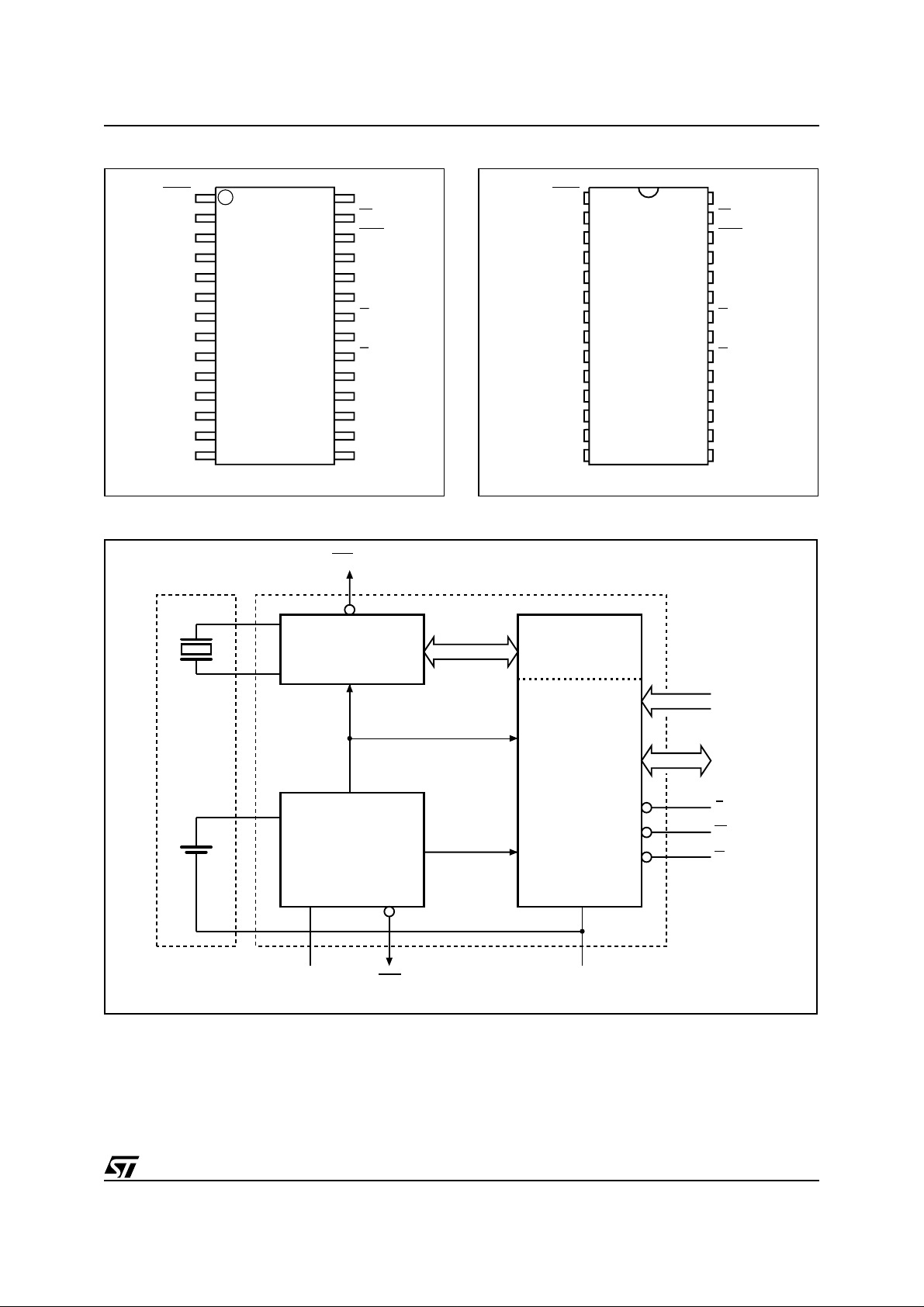
Figure 4. 28-pi n S O I C Co nnections Figure 5. PC DIP 28 CA P H A T Connectio ns
RST V
A12
A7
A6
A5
A4
A3
A2
A1
A0
DQ0
1
2
3
4
5
6
7
8
9
10
11
M48T59Y
M48T59V
12
DQ2
SS
13
14
Figure 6. Block Diagram
32,768 Hz
CRYSTAL
28
27
26
25
24
23
22
21
20
19
18
17
16
15
AI01382E
OSCILLATOR AND
CLOCK CHAIN
CC
W
IRQ/FT
A8
A9
A11
G
A10
E
DQ7
DQ6
DQ5DQ1
DQ4
DQ3V
IRQ/FT
RST V
1
A12
2
A7
3
A6
4
A5
5
A4
6
A3
7
A2
8
A1
9
A0
10
DQ0
11
12
DQ2
13
14
SS
16 x 8 BiPORT
SRAM ARRAY
M48T59
M48T59Y
28
27
26
25
24
23
22
21
20
19
18
17
16
15
AI01381D
CC
W
IRQ/FT
A8
A9
A11
G
A10
E
DQ7
DQ6
DQ5DQ1
DQ4
DQ3V
A0-A12
LITHIUM
CELL
VOLTAGE SENSE
AND
SWITCHING
CIRCUITRY
CC
RSTV
POWER
V
PFD
8176 x 8
SRAM ARRAY
V
SS
DQ0-DQ7
E
W
G
AI01383D
5/29
Page 6
M48T59, M48T59Y, M48T59V*
OPERATION MODES
As Figure 6., page 5 shows, the static memory array and the quartz-controlled clock oscillator of the
M48T59/Y/V are integrated on one silicon chip.
The two circuits are interconnected at the upper
eight memory locations to provide user accessible
BYTEWIDE™ clock information in t he bytes with
addresses 1FF8h-1FFFh. The clock locations
contain the century, year, month, date, day, hour,
minute, and second in 24 hour BCD format (except
for the century). Corrections for 28, 29 (l eap year valid until 2100), 30, and 31 day months are made
automatically. Byte 1FF8h is the clock control register. This byte controls user access to the clock
information and also stores the clock calibration
setting.
The eight clock bytes are not the actual clock
counters themselves; they are memory locations
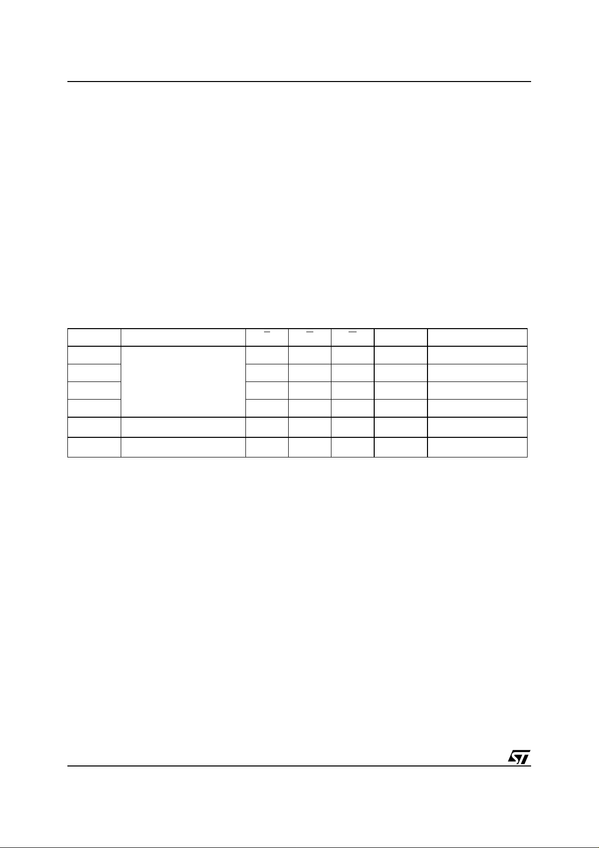
Table 2. Operating Modes
Mode
Deselect
WRITE
READ
READ
Deselect
Deselect
Note: X = VIH or VIL; VSO = Battery B ack-up Switc hover Voltage.
1. See Table 13., page 22 for details.
V
V
4.75 to 5.5V
4.5 to 5.5V
3.0 to 3.6V
to V
SO
PFD
≤ V
or
or
SO
CC
(min)
(1)
(1)
E G W DQ7-DQ0 Power
V
IH
V
IL
V
IL
V
IL
X X X High Z CMOS Standby
X X X High Z Battery Back-up Mode
consisting of BiPORT™ READ/WRITE memory
cells. The M48T59/Y/V includes a clock control circuit which updates the clock bytes with current information once per second. The information can
be accessed by the user in the same manner as
any other location in the static memory array.
The M48T59/Y/V also has its ow n Power-fail Detect circuit. The control circuitry constantly monitors the single 5V/3.3V supply for an out of
tolerance condition. When V
is out of tolerance,
CC
the circuit write protects the SRAM, providing a
high degree of data security in the midst of unpredictable system operation brought on by low V
As V
Voltage (V
falls below the Battery Back-up Switchover
CC
), the control circuitry connects the
SO
battery which maintains data and cloc k operation
until valid power returns.
X X High Z Standby
X
V
IL
V
IH
V
IL
V
IH
V
IH
D
IN
D
OUT
High Z Active
Active
Active
CC
.
6/29
Page 7

READ Mode
The M48T59/Y/V is in the READ M ode whenev er
(WRITE Enable) is high and E (Chip Enable) is
W
low. The unique address specified by the 13 address inputs defines which one of the 8,192 bytes
of data is to be acces sed . Vali d data w ill be av ailable at the Data I/O pi ns within Address Access
time (t
stable, providing that the E
are also satisfied. If the E
) after the last address input signal is
AVQV
and G access times
and G access times are
not met, valid data will be available after the latter
Figure 7. READ Mode AC Waveforms
M48T59, M48T59Y, M48T59V*
of the Chip Enable Access time (t
Enable Access time (t
GLQV
).
The state of the eight t hree-state Da ta I/O si gnals
is controlled by E
ed before t
indeterminate state until t
puts are changed while E
and G. If the outputs are activat-
, the data lines will be driven to an
AVQV
AVQV
and G remain active,
output dat a will re main valid for Ou tput D ata H old
time (t
) but will go indeterminate until the next
AXQX
Addr e ss Access.
tAVAV
ELQV
. If the Ad dres s In-
) or Output
A0-A12
tAVQV tAXQX
tELQV
E
tELQX
tGLQV
G
tGLQX
DQ0-DQ7
Note: W RITE Enable (W) = High.
VALID
tEHQZ
tGHQZ
VALID
AI01385
Table 3. READ Mode AC Characteristics
M48T59/Y/V
Symbol
t
AVAV
t
AVQV
t
ELQV
t
GLQV
t
ELQX
t
GLQX
t
EHQZ
t
GHQZ
t
AXQX
Note: 1. Valid for Ambient Operating Temperat ure: TA = 0 to 70°C; VCC = 4.5 to 5.5V, 4.7 5 to 5.5V, or 3.0 to 3.6V (except where noted) .
2. C
3. C
READ Cycle Time 70 ns
(2)
Address Valid to Output Valid 70 ns
(2)
Chip Enable Low to Output Valid 70 ns
(2)
Output Enable Low to Output Valid 35 ns
(3)
Chip Enable Low to Output Transition 5 ns
(3)
Output Enable Low to Output Transition 5 ns
(3)
Chip Enable High to Output Hi-Z 25 ns
(3)
Output Enable High to Output Hi-Z 25 ns
(2)
Address Transition to Output Transition 10 ns
= 100pF (see Figure 15 .,page 20).
L
= 5pF (see Figure 15., page 20).
L
Parameter
(1)
Unit–70
Min Max
7/29
Page 8
M48T59, M48T59Y, M48T59V*
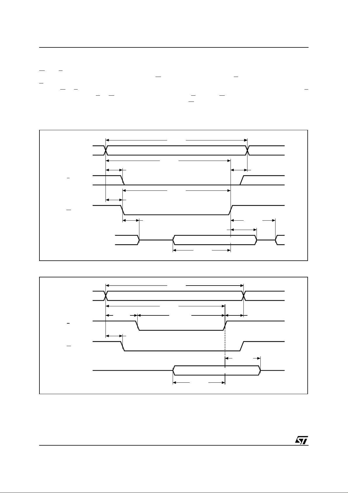
WRITE Mode
The M48T59/Y/V is in the WRITE Mode whenever
and E are low. The start of a WRITE is refer-
W
enced from the latter occurring falling edge of W
. A WRITE is terminated by the earlier rising
E
edge of W
throughout the cycle. E
a minimum of t
or E. The addresses must be held valid
or W must return high for
from Chip Enable or t
EHAX
or
WHAX
from WRITE Enable prior to the initiation of anoth-
Figure 8. WRITE Enable Controlled, WRITE Mode AC Waveforms
er READ or WRITE cycle. Data-in must be valid
t
for t
prior to the end of WRITE and remain valid
DVWH
afterward. G should be kept high during
WHDX
WRITE cycles to avoid bus contention; however, if
the output bus has b een activated by a low on E
and G a low on W will disable the outputs t
falls .
ter W
tAVAV
WLQZ
af-
A0-A12
tAVEL
E
tAVWL
W
tWLQZ
DQ0-DQ7
VALID
tAVWH
tWLWH
DATA INPUT
tDVWH
Figure 9. Chip Enable Controlled, WRITE Mode AC Waveforms
tAVAV
A0-A12
tAVEL
VALID
tAVEH
tELEH
tWHAX
tWHQX
tWHDX
AI01386
tEHAX
8/29
E
W
DQ0-DQ7
tAVWL
tDVEH
tEHDX
DATA INPUT
AI01387B
Page 9

M48T59, M48T59Y, M48T59V*
Table 4. WRITE Mode AC Characteristics
M48T59/Y/V
Symbol
Parameter
(1)
Min Max
t
AVAV
t
AVWL
t
AVEL
t
WLWH
t
ELEH
t
WHAX
t
EHAX
t
DVWH
t
DVEH
t
WHDX
t
EHDX
(2,3)
t
WLQZ
t
AVWH
t
AVEH
(2,3)
t
WHQX
Note: 1. Valid for Ambient Operating Temperat ure: TA = 0 to 70°C; VCC = 4.5 to 5.5V, 4.7 5 to 5.5V, or 3.0 to 3.6V (except where noted) .
= 5pF (see Figure 15., page 20).
2. C
L
3. If E
WRITE Cycle Time 70 ns
Address Valid to WRITE Enable Low 0 ns
Address Valid to Chip Enable Low 0 ns
WRITE Enable Pulse Width 50 ns
Chip Enable Low to Chip Enable High 55 ns
WRITE Enable High to Address Transition 0 ns
Chip Enable High to Address Transition 0 ns
Input Valid to WRITE Enable High 30 ns
Input Valid to Chip Enable High 30 ns
WRITE Enable High to Input Transition 5 ns
Chip Enable High to Input Transition 5 ns
WRITE Enable Low to Output Hi-Z 25 ns
Address Valid to WRITE Enable High 60 ns
Address Valid to Chip Enable High 60 ns
WRITE Enable High to Output Transition 5 ns
goes low simultaneously with W going low , t he outputs remai n in the high impedance state.
Unit–70
9/29
Page 10

M48T59, M48T59Y, M48T59V*
Data Retention Mode
With valid V
as a conventional BYTEWIDE™ static RAM.
Should the supply voltage decay, the RAM will automatically power-fail deselect, write protecting itself when V
(min) window. All outputs become high impedance, and all inputs are treated as “don't care.”
Note: A power failure during a WRITE cycle may
corrupt data at the currently a ddressed location,
but does not jeopardize the rest of the RAM's content. At voltages below V
assured the memory will be i n a write protected
state, provided the V
The M48T59/Y/V may respond to transient noise
spikes on V
during the time the device is sampling V
fore, decoupling of the power supply lines is recommended.
applied, the M48T59/ Y/V operat es
CC
falls within the V
CC
(min), the user can be
PFD
fall time is not less than tF.
CC
that reach into the deselect window
CC
PFD
(max ), V
. There-
CC
PFD
When V
drops below VSO, the control circuit
CC
switches power to the internal battery which preserves data and powers the clock. The internal
button cell will maintain data in the M48T59/Y/V for
an accumulated period of at least 7 years when
is less than VSO. As system power returns
V
CC
and V
rises above VSO, the battery is disc on-
CC
nected and the power supply is switch ed to ex ternal V
. Deselect continues for t
CC
reaches V
PFD
(max).
after V
rec
CC
For more information on Battery Storage Life refer
to the Application Note AN1012.
10/29
Page 11

CLOCK OPERATIONS
Reading the Clock
Updates to the TIMEKEEPER
be halted before clock data is read to prevent
reading data in transition. The BiPORT ™ TIMEKEEPER cel ls in the R AM a r ra y are only d ata registers and not the actual clock counters, so
updating the registers can be halted without disturbing the clock itself.
Updating is halted when a '1' is written to the
READ Bit, D6 in the Control regi ster (1FF8h). As
long as a '1' remains in that position , updating is
halted. After a h alt is issu ed, the registers reflect
the count; that is, the day, date, and the time that
were current at the moment the halt command was
issued.
All of the TIMEKEEPER registers are updated simultaneously. A halt will not interrupt an update in
progress. Updating is within a second after the bit
is reset to a '0.'
Setting the Clock
Bit D7 of the Control register (1FF8h) is the
WRITE Bit. Setting the WRITE Bit to a '1,' like the
READ Bit, halts updates to the TIMEKEEPER registers. The user can then load t hem with the correct day, date, and time data in 24 hour BCD
format (see Table 5., page 12). Resetting the
WRITE Bit to a '0' then transfers the values of all
time registers (1FF9h-1FFFh) to the actual TIME-
®
registers should
M48T59, M48T59Y, M48T59V*
KEEPER counters and allows normal operation to
resume. After the WRITE Bit is reset, the next
clock update will occur within approximately one
second.
See the Application Note AN923, “TIMEKEEPER
Rolling Into the 21st Centu ry” for information on
Century Rollover.
Note: Upon power-up following a power failure,
both the WRITE Bit and the READ Bit will be reset
to '0.'
Stopping and Starting the Oscillator
The oscillator may be stopped at any time. If the
device is going to spend a significant amount of
time on the shelf, the oscillator can be turned off to
minimize current drain on the battery. The STOP
Bit is the MSB of the seconds register. Setting it to
a '1' stops the oscillator. The M48T59/Y/V in the
DIP package is shipped from STM icroelectronics
with the STOP Bit set to a '1.' When reset to a '0,'
the M48T59/Y/V oscillato r starts within o ne second.
Note: It is not necessary to set the WRITE Bit
when setting or resetting the FREQUENCY TEST
Bit (FT), the STOP Bit (ST) or the CENTURY ENABLE Bit (CE B).
11/29
Page 12
M48T59, M48T59Y, M48T59V*
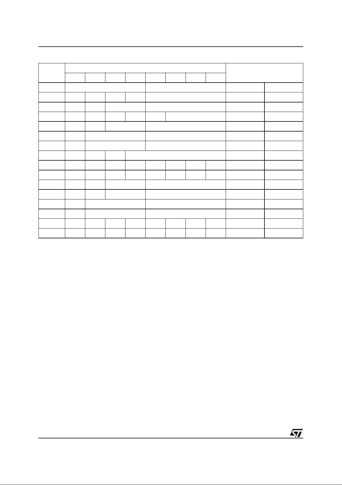
Table 5. Register Map
Address
Data
D7 D6 D5 D4 D3 D2 D1 D0
1FFFh 10 Years Year Year 00-99
1FFEh 0 0 0 10 M Month Month 01-12
1FFDh 0 0 10 Date Date Date 01-31
1FFCh 0 FT CEB CB 0 Day Century/Day 00-01/01-07
1FFBh 0 0 10 Hours Hours Hours 00-23
1FFAh 0 10 Minutes Minutes Minutes 00-59
1FF9h ST 10 Seco nds Seconds Seconds 00-59
1FF8h W R S Calibration Control
1FF7h WDS BMB4 BMB3 BMB2 BMB1 BMB0 RB1 RB0 Watchdog
1FF6hAFEYABEYYYYYInterrupts
1FF5h RPT4 Y Al. 10 Date Alarm Date Alarm Date 01-31
1FF4h RPT3 Y Al. 10 Hours Alarm Hours Alarm Hours 00-23
1FF3h RPT2 Alarm 10 Minutes Alarm Minutes Alarm Minutes 00-59
1FF2h RPT1 Alarm 10 Seconds Alar m Seco nds A lar m Secon ds 00-59
Function/Range
BCD Format
1FF1hYYYYYYYY Unused
1FF0h WDF AF Z BL Z Z Z Z Flags
Keys : S = SIG N Bit
FT = FREQUENCY TEST Bit
R = READ Bit
W = WRITE B i t
ST = STOP Bit
0 = Must be set to '0'
Y = '1' or '0'
Z = '0' and are Read only
AF = Alarm Flag (Read only)
BL = Battery Low (Read only)
WDS = Watchdog Steeri ng B i t
BMB0-BMB4 = Watchdog Multiplier Bits
RB0-RB 1 = Watchdog Resolution Bit s
AFE = Alarm Flag Enable
ABE = Alarm in Battery Back-up Mode Enable
RPT1-RP T 4 = Alarm Repeat Mode Bits
WDF = Watchdog Flag (R ead only)
CEB = Centur y E nable Bit
CB = Centur y B i t
12/29
Page 13

Calibrating the C lock
The M48T59/Y/V is driven by a quartz-controlled
oscillator with a nominal frequency of 32,768 Hz.
The devices are tested not to exceed 35 PPM
(parts per million) oscillator frequency error at
25°C, which equates to about ±1. 53 minutes per
month. With the calibration bits properly set, the
accuracy of each M48T59/Y/V improve s to better
than +1/–2 PPM at 25°C.
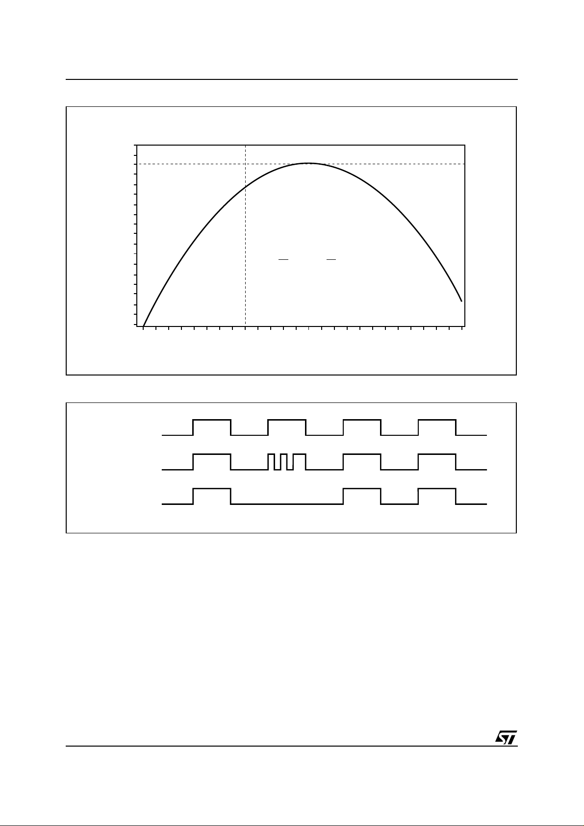
The oscillation rate of any crystal changes with
temperature (see Figure 10., page 14). Most clock
chips compensate for crystal frequency and temperature shift error with cumbersome “trim” capacitors. The M48T59/Y/V design, however, employs
periodic counter correction. The calibration circuit
adds or subtracts counts from the oscillator divider
circuit at the divide by 256 stage, as shown in Fig-
ure 11., page 14. The number of time s pulses are
blanked (subtracted, negat ive calibration) or split
(added, positive calibration) depends upon the
value loaded into the five-bit Calibration byte found
in the Control Register. Adding counts speeds the
clock up, subtracting counts slows the clock down.
The Calibration Byte occupies the five lower order
bits (D4-D0) in the Control register (1FF8h). These
bits can be set to represent any value between 0
and 31 in binary form. Bit D5 is the Sign Bit; '1' indicates positive calibration, '0' indicates negat ive
calibration. Calibration occurs within a 64 m inute
cycle. The first 62 m inut es i n t he c ycle m ay , once
per minute, have one second either shortened by
128 or lengthened by 256 oscillator cycles. If a binary '1' is loaded into the register, only the first 2
minutes in the 64 minute cycle will be modified; if
a binary 6 is loaded, the first 12 will be affected,
and so on.
Therefore, each calibration step has t he effect of
adding 512 or subtracting 256 oscillator cycles; for
every 125,829,120 actual oscillator cycles, that is
+4.068 or –2.034 PPM of adjustment per calibration step in the calibrat ion registe r. Assum ing that
M48T59, M48T59Y, M48T59V*
the oscillator is in fact running at exactly 32,768
Hz, each of the 31 increm ents in the Calibration
Byte would represent +10.7 or –5. 35 se conds per
month which corresponds to a total range of +5.5
or –2.75 minutes per month.
Two methods are available for ascertaining how
much calibration a given M48T59/Y/V may require. The first involves simply setting the clock,
letting it run for a month and comparing it to a
known accurate reference (like WWV broadcasts).
While that may seem crude, it allows the designer
to give the end user the ability to calibrate his clock
as his environment may require, even after the final product is packaged in a non-user serviceable
enclosure. All the des igner has to d o is provide a
simple utility that accesses the Calibration Byte.
The second approach is better suited t o a manufacturing environment, and involves the use of the
FT pin. The pin will toggle at 512 Hz when the
IRQ/
Stop Bit (D7 of 1FF9h) is '0,' the FT Bit (D6 of
1FFCh) is '1,' the AFE Bit (D7 of 1FF6h) is '0,' and
the Watchdog Steering Bit (D7 of 1FF7h) is '1' or
the Watchdog Register is reset (1FF7h = 0).
Any deviation from 512 Hz indicates the degree
and direction of oscillator frequency shift at the test
temperature. For example, a reading of 512.01024
Hz would indicate a +20 PPM oscillator frequency
error, requiring a –10 (WR001010) to be loaded
into the Calibration Byte for correction. Note that
setting or changing the Calibration Byte does not
affect the Frequency Test output frequency.
The IRQ
quires a pull-up resistor for proper operation. A
500-10kΩ resistor is recommended in order to
control the rise time. The FT Bit is cleared on power-down.
For more information on c alibration, see Application Note AN934, “TIMEKEEPER Calib ra t i on.”
/FT pin is an open drain output which re-
13/29
Page 14
M48T59, M48T59Y, M48T59V*
Figure 10. Crystal Accuracy Across Temp eratur e
Frequency (ppm)
20
0
–20
–40
–60
–80
–100
–120
–140
–160
0 10203040506070
∆F
F
Temperature °C
= -0.038 (T - T
ppm
2
C
T0 = 25 °C
)2 ± 10%
0
80–10–20–30–40
AI00999
Figure 11. Cl ock Ca l ib rat i on
NORMAL
POSITIVE
CALIBRATION
NEGATIVE
CALIBRATION
AI00594B
14/29
Page 15
Setting the Alarm Clock
Registers 1FF5h-1FF2h contain the alarm settings. The alarm can be configured to go off at a
prescribed time on a specific day of the month or
repeat every month, day, hour, minute, or second.
It can also be programmed to go off while the
M48T59/Y/V is in the battery back-up mode of operation to serve as a system wake-up call.
Bits RPT1-RPT4 put the alarm in the repeat mode
of operation. Table 6., page 15 shows the possible
configurations. Codes not listed in the table default
to the once per second mode to quickly alert the
user of an incorrect alarm setting.
Note: User must transition address (or toggle chip
enable) to see Flag Bit change.
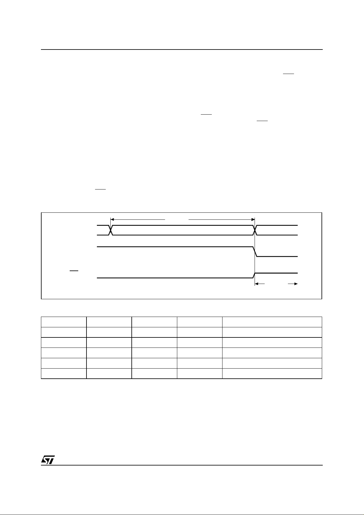
When the clock information matches the alarm
clock settings based on the m atch criteria d efined
by RPT1-RPT4, AF (Alarm Flag) is set. If AFE
(Alarm Flag Enable) is also set, the alarm condition activates the IRQ
/FT pin. To disable the
Figure 12. Alarm Interrupt Reset Waveform
15ns Min
M48T59, M48T59Y, M48T59V*
alarm, write '0' to the Alarm Date Register and
RPT1-4. The Alarm Flag and the IRQ
are cleared by a READ to the Flags Register as
shown in Figure 12., page 15. A subsequent
READ of the Flags Register is necessary to see
that the value of the Alarm Flag has been reset to
'0.'
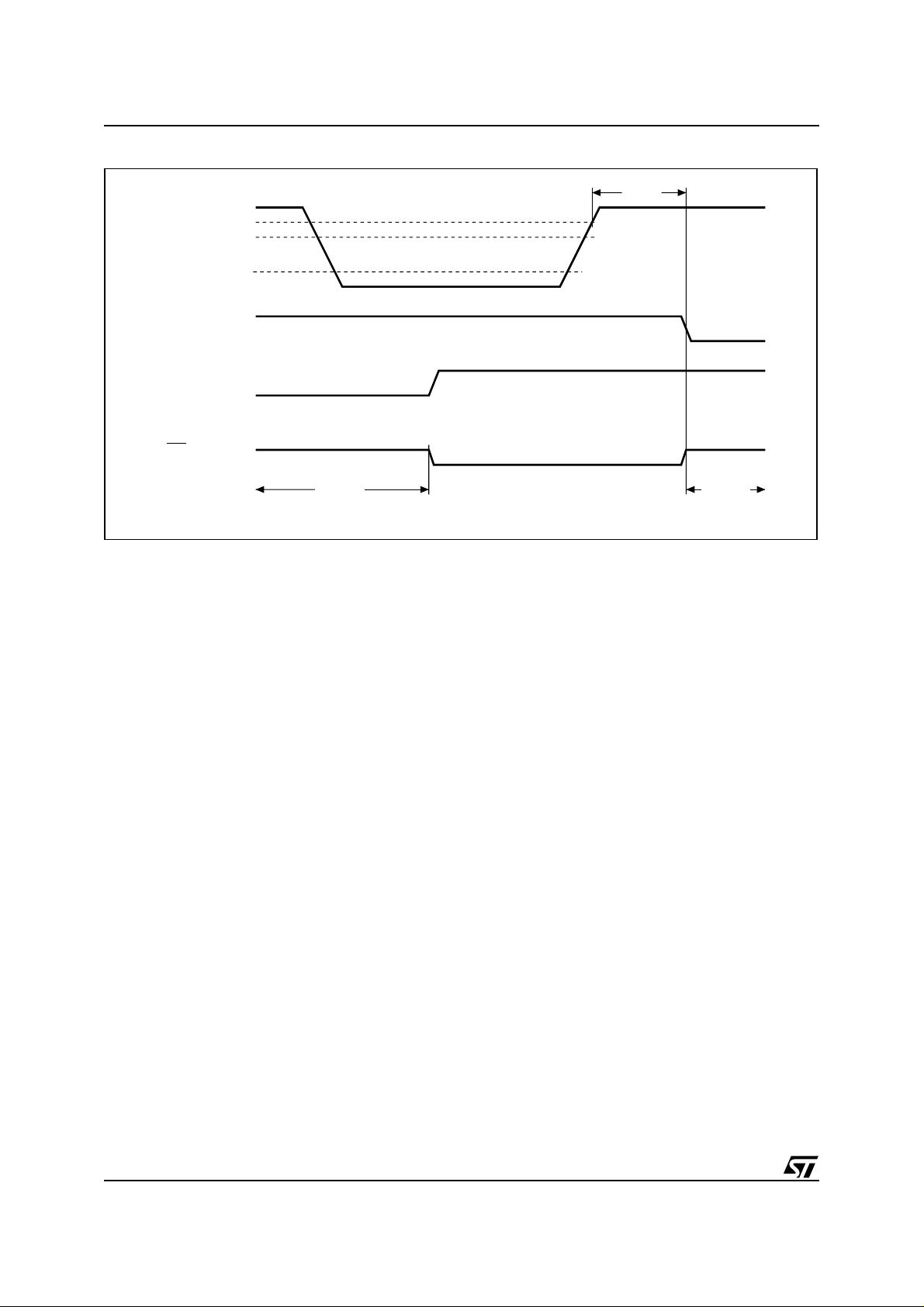
The IRQ
tery back-up mode. The IRQ
/FT pin can also be activated in the bat-
/FT will go low if an
alarm occurs and both the ABE (Alarm in Battery
Back-up Mode Ena ble) and the AFE are set. The
ABE and AFE bits are reset during power-up,
therefore an alarm generated during power-up will
only set AF. The user can read the Flag Register
at system boot-up to determine if an alarm was
generated while the M48T59/Y/V was in the deselect mode during power-down. Figure
13., page 16 illustrates the back-up mode alarm
timing.
/FT output
A0-A12
ACTIVE FLAG BIT
IRQ/FT
ADDRESS 1FF0h
Table 6. Alarm Repeat Mode
RPT4 RPT3 RPT2 RPT1 Alarm Activated
1111 Once per Second
1110 Once per Minute
1100 Once per Hour
1000 Once per Day
0000 Once per Month
HIGH-Z
AI01388B
15/29
Page 16
M48T59, M48T59Y, M48T59V*
Figure 13. Back-up Mode Alarm Waveforms
V
CC
V
(max)
PFD
V
(min)
PFD
V
SO
ABE, AFE bit in Interrupt Register
AF bit in Flags Register
IRQ/FT
HIGH-Z
trec
HIGH-Z
AI03254B
16/29
Page 17

Watchdog Timer
The watchdog timer can be used to detect an outof-control microprocessor. The user programs the
watchdog timer by setting the desired amount of
time-out into the eight-bit Watchdog Register (Address 1FF7h). The five bits (BMB4-BMB0) that
store a binary multiplier and the two lower order
bits (RB1-RB0) select the resolution, where
00 = 1/16 second, 01 = 1/4 second, 10 = 1 second, and 11 = 4 seconds. The amount of time-out
is then determined to be the multiplication of the
five-bit multiplier value with the resolution. (For example: writing 00001110 in the Watchdog Register = 3 x 1 or 3 seconds).
Note: Accuracy of timer is within ± the selected
resolution.
If the processor does not reset the timer within the
specified period, the M48T59/Y/V sets the WDF
(Watchdog Flag) and generates a watchdog interrupt or a microprocessor reset. WDF is reset by
reading the Flags Register (Address 1FF0h).
Note: User must transition address (or toggle chip
enable) to see Flag Bit change.
The most significant bit of the Watchdog Register
is the Watchdog Steering Bit. When set to a '0,' the
watchdog will activate the IRQ
/FT pin when timedout. When WDS is set to a '1,' the watchdog will
output a negative pulse on the RST
tion of t
. The Watchdog Register, the FT Bit, and
rec
pin for a dura-
the AFE and ABE Bits will reset to a '0' at the end
of a watchdog time-out when the WDS bit is set to
a '1.'
The watchdog timer resets when the microprocessor performs a re-write of the Watchdog Register.
The time-out period then st arts over. The watchdog timer is disabled by writing a value of
00000000 to the eight bits in the Watchdog Register.
The watchdog function is automatically disabled
upon power-down and the Watchd og Register is
cleared. If the watchdog function is set to output to
the IR Q
/FT pin and the frequency tes t function is
activated, the watchdog or alarm function prevails
and the frequency test function is denied.
Power-on Reset
The M48T59/Y/V continuously monitors V
When V
the RST
power-up for t
RST
falls to the power fail detect trip point,
CC
pulls low (open drain) and remains low on
after VCC passes V
rec
PFD
is valid for all VCC conditions. The RST pin is
CC
(max).
an open drain output and an appropriate resistor to
should be chosen to control rise time.
V
CC
Programmable Interrupts
The M48T59/Y/V provides two prog rammable interrupts; an alarm and a watchdog. When an interrupt condition occurs, the M48T59/Y/V sets the
M48T59, M48T59Y, M48T59V*
appropriate flag bit in the Flag Register 1FF0h.
The interrupt enable bits in (AFE and ABE) in
1FF6h and the Watchdog Stee ring (WDS) Bit in
1FF7h allow the interrupt to activate the IRQ
pin.
The Alarm flag and the IRQ
by a READ to the Flags Register. An interrupt condition reset will not occur unless the addresses are
stable at the flag location for at least 15ns whi le
the device is in the READ Mode as shown in Fig-
ure 12., page 15.
The IRQ
/FT pin is an open drain output and re-
quires a pull-up resistor (10kΩ recommended) t o
. The pin remains in the high impedance state
V
CC
unless an interrupt occurs or the Frequency T est
Mode is enabled.
Battery Low Fl ag
The M48T59/Y/V automatically performs periodic
battery voltage monitoring upon power-up and at
factory-programmed time intervals of 24 hours (at
day rollover) as long as the device is powered and
the oscillator is running. The Battery Low Flag
(BL), Bit D4 of the Flags Regi ster 1FF0 h, will be
asserted high if the internal or SNAPHAT
is found to be l ess than approx imately 2.5V. T he
BL Flag w ill r ema in a ctive u ntil com plet ion o f ba ttery replacement and subsequent battery low
monitoring tests, either during the next power-up
sequence or the next scheduled 24-hour interval.
If a battery low is generated during a power-up sequence, this indicates that the battery v oltage is
below 2.5V (approximately), which may be insufficient to maintain data integrity. Data should be
considered suspect and verified as correct. A fresh
battery should be installed.
If a battery low indication is generated during the
24-hour interval check, this indicates the battery is
near end of life. However, data has not been compromised due to the fact that a nominal V
plied. In order to insure data integrity during
subsequent periods of b attery bac k-up mode, it is
recommended that the battery be replaced. The
SNAPHAT top may be replaced while V
plied to the device.
Note: This will cause the clock to lose time during
.
the interval the battery/crystal is removed.
Note: Battery monitoring is a useful technique only
when performed periodically. The M48T59/Y/V
only monitors the battery when a nominal V
applied to the device. Thus applications which require extensive durations in the battery back-up
mode should be powered-up periodically (at least
once every few months) in order for this technique
to be beneficial. Additionally, if a battery low is indicated, data integrity should be verified upon
power-up via a checksum or other technique.
/FT output are cleared
®
battery
is sup-
CC
is ap-
CC
CC
/FT
is
17/29
Page 18
M48T59, M48T59Y, M48T59V*
Century Bit
Bit D5 and D4 of Clock Register 1FFCh contain
the CENTURY ENABLE Bit (CEB) and the CENTURY Bit (CB). Setting CEB to a '1' will cause CB
to toggle, either from a '0' to '1' or from '1' to '0' at
the turn of the century (depending upon its initial
state). If CEB is set to a '0,' CB will not toggle.
Note: The WRITE Bit mu st be set in order to wri te
to the CENTURY Bit.
Table 7. Default Values
Condition W R FT AFE ABE
Initial Power-up
(Battery Attach for SNAPHAT)
Subsequent Power-up / RESET
Power-down
Note: 1 . WDS, BMB0-BMB4, RBO, RB 1.
(4)
2. State of other control bits undefined.
3. State of other control bits rem ains unchanged.
4. Ass um i ng these bits set to '1' prior t o power-down.
(2)
(3)
00000 0
00000 0
00011 0
VCC Noise And Negative Going Transients
transients, including those produced by output
I
CC
switching, can produce voltage fluctuations, resulting in spikes on the V
bus. These transients
CC
can be reduced if capacitors are used to store energy which stabilizes the V
bus. The energy
CC
stored in the bypass capacitors will be released as
low going spikes are generated or energy will be
absorbed when overshoots occur. A ceramic bypass capacitor value of 0.1µF (as shown in Figure
14.) is recommended in order to provide the need-
ed filtering.
In addition to transients that are caused by normal
SRAM operation, power cycling can generate negative voltage spikes on V
below V
by as much as one volt. These negative
SS
that drive it to values
CC
spikes can cause data corruption in the SRAM
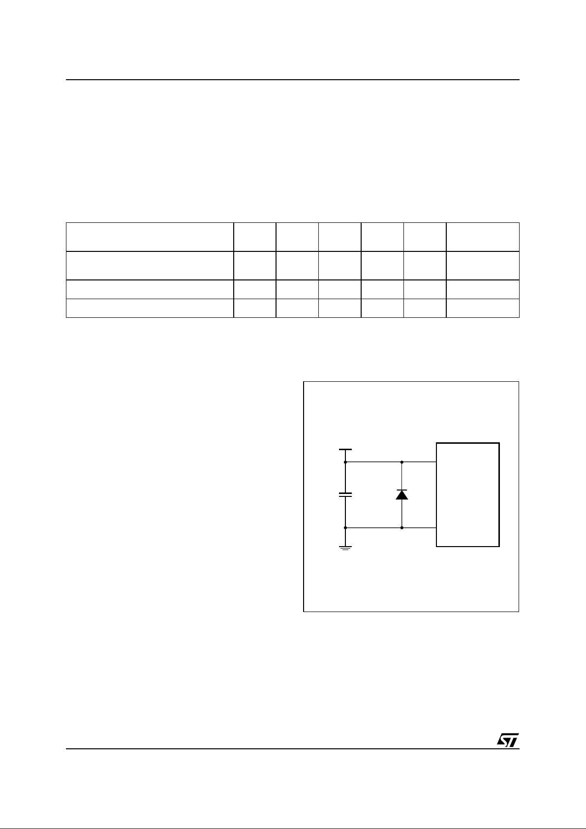
while in battery backup mode. To protect from
these voltage spikes, it is recommended to connect a schottky diode from V
connected to V
, anode to VSS). Schottky diode
CC
to VSS (cathode
CC
1N5817 is recommended for through hole and
MBRS120T3 is recommended for surface mount.
Initi a l Powe r-on Defaul ts
Upon application of power to the de vice, the following register bits are set to a '0' state: WDS;
BMB0-BMB4 ; RB0-RB1; AFE; ABE; W; R; FT (see
Table 7.).
WATCHDOG
Register
(1)
Figure 14. Supply Voltage Protection
V
CC
V
CC
0.1µF DEVICE
V
SS
AI02169
18/29
Page 19
M48T59, M48T59Y, M48T59V*
MAXIMUM RA T ING
Stressing the device above the rating l isted in the
“Absolute Maximum Ratings” table may cause
permanent damage to the device. These are
stress ratings only and operation of the device at
these or any other conditions above those indicated in the Operating sections of this specification is
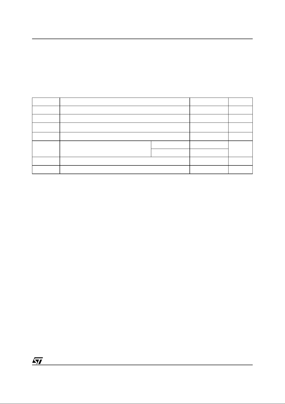
Table 8. Absolute Maximum Ratings
Symbol Parameter Value Unit
not implied. Exposure to Absol ute Max imum Ra ting conditions for extended periods may affect device reliability. Refer also to the
STMicroelectronics SURE Program and other relevant quality documents.
T
A
T
STG
(1,2,3)
T
SLD
V
IO
Ambient Operating Temperature 0 to 70 °C
Storage Temperature (VCC Off, Oscillator Off)
–40 to 85 °C
Lead Solder Temperature for 10 seconds 260 °C
Input or Output Voltages –0.3 to 7 V
M48T59/M48T59Y –0.3 to 7
V
CC
I
O
P
D
Note: 1. For DIP package: Soldering temperature not to exceed 260°C for 10 seconds (total thermal budget not to exceed 150°C for longer
than 30 seconds).
2. For S O package, st andard (SnPb) lead finish: Reflo w at peak temperature of 225°C (total thermal budget not to exc eed 180°C fo r
between 90 to 15 0 s e c o nds).
3. For S O package , Lead-free (Pb-free) lead fin i sh: Reflow at peak temperature of 260°C (total thermal budge t not to exc eed 245°C
for greater than 30 seconds).
CAUTION: Negative und ershoots be l ow –0.3V are no t all owed on any pin whi l e i n the Batter y Back-up mo de.
CAUTION: Do NOT wave solder SOIC to avoid damaging SNAPHAT sockets.
Supply Voltage
V
M48T59V –0.3 to 4.6
Output Current 20 mA
Power Dissipation 1 W
19/29
Page 20
M48T59, M48T59Y, M48T59V*
DC AND AC PARAMETERS
This section summarizes the operating and measurement conditions, as well as the DC and AC
characteristics of the device. The parameters in
the following DC and AC Characteristic tables are
derived from tests performed under the Meas ure-
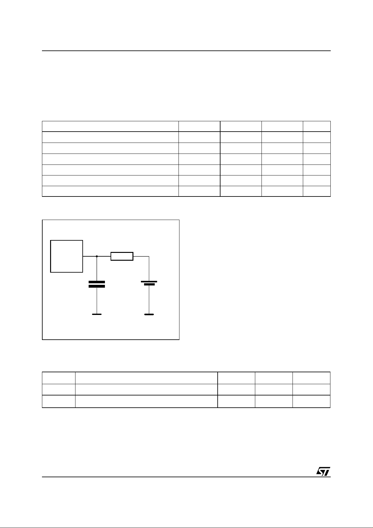
Table 9. Operating and AC Measurement Conditions
Parameter M48T59 M48T59Y M48T59V Unit
ment Conditions listed in t he relevant tables. Designers should check that the operating conditions
in their projects match the measurement conditions when using the quoted parameters.
Supply Voltage (V
Ambient Operating Temperature (T
Load Capacitance (C
CC
)
)
A
)
L
4.75 to 5.5 4.5 to 5.5 3.0 to 3.6 V
0 to 70 0 to 70 0 to 70 °C
100 100 50 pF
Input Rise and Fall Times ≤ 5 ≤ 5 ≤ 5ns
Input Pulse Voltages 0 to 3 0 to 3 0 to 3 V
Input and Output Timing Ref. Voltages 1.5 1.5 1.5 V
Note: Output Hi-Z is defined as the point where data is no longer driven.
Figure 15. AC Measureme nt Load Circui t
DEVICE
UNDER
TEST
645Ω
CL = 100pF
(1)
1.75V
CL includes JIG capacitance
Note: Excluding open-drain output pins
1. 50pF for M48T59V.
AI02325
Table 10. Capacitance
Symbol
C
IN
C
IO
Note: 1. Effec tive capacit ance measured with power suppl y at 5V; sampled only, not 100 % t ested.
2. At 25° C, f = 1MHz.
3. Outputs deselect ed.
Input Capacitance 10 pF
(3)
Input / Output Capacitance 10 pF
Parameters
20/29
(1,2)
Min Max Unit
Page 21
M48T59, M48T59Y, M48T59V*
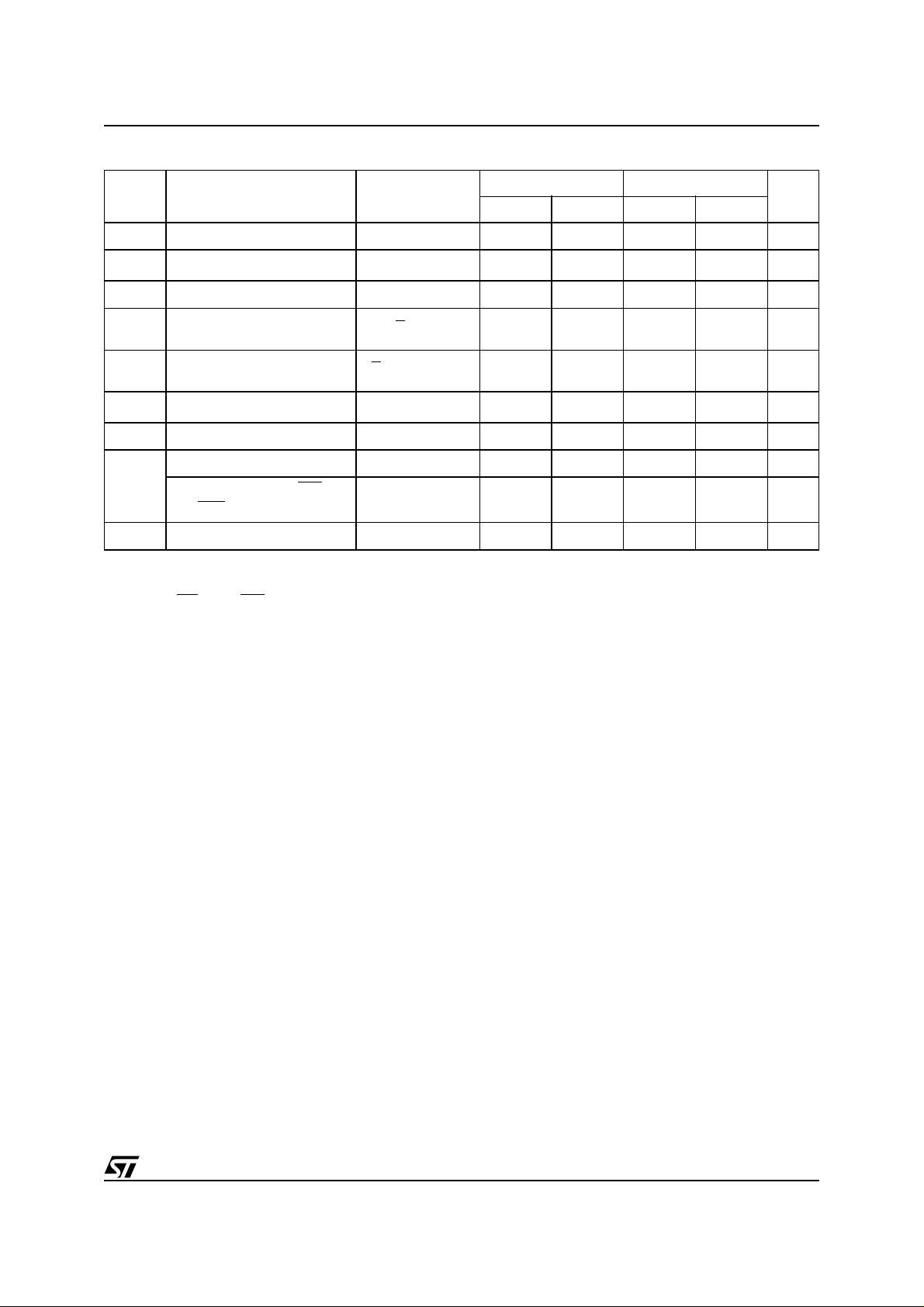
Table 11. DC Characteristics
M48T59/Y M48T59V
Min Max Min Max
±1 ±1 µA
±1 ±1 µA
32mA
31mA
V
CC
+ 0.3
2
VCC + 0.3
0.4 0.4 V
0.4 0.4 V
2.4 2.4 V
Unit
V
IN
≤ V
≤ V
IH
(1)
CC
CC
Symbol Parameter
I
Input Leakage Current
LI
(2)
I
LO
I
I
V
V
Output Leakage Current
I
Supply Current Outputs open 50 30 mA
CC
Supply Current (Standby)
CC1
TTL
Supply Current (Standby)
CC2
CMOS
(3)
Input Low Voltage –0.3 0.8 –0.3 0.8 V
IL
Input High Voltage 2.2
IH
Output Low Voltage
V
OL
Output Low Voltage (IRQ
and RST
V
Note: 1. Valid for Ambient Operating Temperat ure: TA = 0 to 70°C; VCC = 4.5 to 5.5V, 4.7 5 to 5.5V, or 3.0 to 3.6V (except where noted) .
Output High Voltage
OH
2. Outputs deselect ed.
3. Nega t i ve spike s of –1 V al l owed for up t o 10 ns once per cycle.
4. The I RQ
(4)
)
/FT and RST pins are Open Drain.
/FT
Test Condition
0V ≤ V
0V ≤ V
OUT
= V
E
= VCC – 0.2V
E
I
= 2.1mA
OL
IOL = 10mA
I
= –1mA
OH
21/29
Page 22
M48T59, M48T59Y, M48T59V*
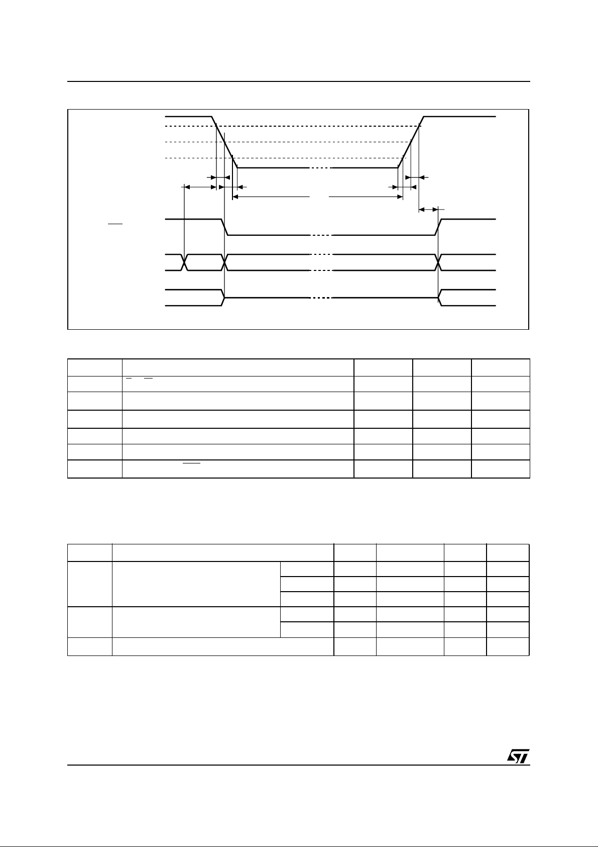
Figure 16. Power Down/Up Mode AC Waveforms
V
CC
V
(max)
PFD
V
(min)
PFD
VSO
RST
INPUTS
OUTPUTS
tPD
(PER CONTROL INPUT) (PER CONTROL INPUT)
tF
RECOGNIZED RECOGNIZED
VALID VALID
tFB
tDR
tRB
DON'T CARE
HIGH-Z
tR
trec
AI03258
Table 12. Power Down/Up AC Characteristics
Symbol
t
PD
(2)
t
F
t
FB
t
R
t
RB
t
rec
Note: 1. Valid for Ambient Operating Temperat ure: TA = 0 to 70°C; VCC = 4.5 to 5.5V, 4.7 5 to 5.5V, or 3.0 to 3.6V (except where noted) .
2. V
3. V
E or W at VIH before Power Down
V
(max) to V
PFD
(3)
V
(min) to VSS VCC Fall Time
PFD
V
(min) to V
PFD
VSS to V
V
PFD
(max) to V
PFD
(min).
es V
PFD
(min) to VSS fall time of less than tFB may cause corruption of RA M data.
PFD
(min) VCC Rise Time
PFD
(max) to RST High
(min) fall time of less than tF may result in deselection/write protection not occurring until 200µs after VCC pass-
PFD
Parameter
(min) VCC Fall Time
PFD
(max) VCC Rise Time
PFD
(1)
Min Max Unit
0µs
300 µs
10 µs
10 µs
1µs
40 200 ms
Table 13. Power Down/Up Trip Points DC Characteristics
Symbol
Parameter
(1,2)
M48T59 4.5 4.6 4.75 V
V
PFD
Power-fail Deselect Voltage
M48T59Y 4.2 4.35 4.5 V
M48T59V 2.7 2.9 3.0 V
V
t
DR
Note: 1. Valid for Ambient Operating Temperat ure: TA = 0 to 70°C; VCC = 4.5 to 5.5V, 4.7 5 to 5.5V, or 3.0 to 3.6V (except where noted) .
Battery Back-up Switchover Voltage
SO
(3)
Expected Data Retention Time 7 YEARS
2. All voltages referenced to V
3. At 25° C, V
CC
= 0V.
SS
.
M48T59/Y 3.0 V
M48T59V
22/29
Min Typ Max Unit
V
PFD
–100mV
V
Page 23
M48T59, M48T59Y, M48T59V*
PACKAG E MECHANICA L INFORMATION
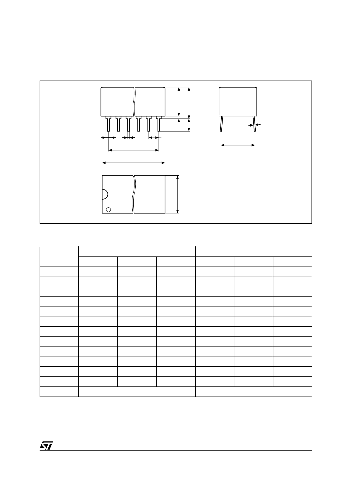
Figure 17. PCDIP28 – 28-pin Plastic DIP, battery CAPHAT, Package Outline
A2
B1 B
A1AL
e1
C
eA
e3
D
N
E
1
Note: Drawing is not to scale.
PCDIP
Table 14. PCDIP28 – 28-pin Plastic DIP, battery CAPHAT, Package Mechanical Data
Symb
Typ Min Max Typ Min Max
A 8.89 9.65 0.350 0.380
A1 0.38 0.76 0.015 0.030
A2 8.38 8.89 0.330 0.350
B 0.38 0.53 0.015 0.021
mm inches
B1 1.14 1.78 0.045 0.070
C 0.20 0.31 0.008 0.012
D 39.37 39.88 1.550 1.570
E 17.83 18.34 0.702 0.722
e1 2.29 2.79 0.090 0.110
e3 29.72 36.32 1.170 1.430
eA 15.24 16.00 0.600 0.630
L 3.05 3.81 0.120 0.150
N 28 28
23/29
Page 24
M48T59, M48T59Y, M48T59V*
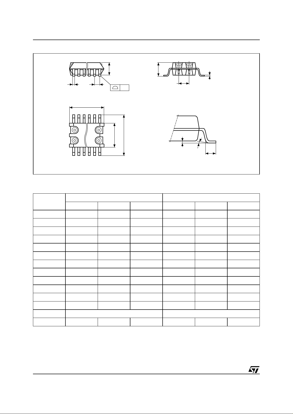
Figure 18. SOH28 – 28-lead Plastic Small Outline, battery SNAPHAT, Package Outline
A2
A
C
Be
eB
CP
D
N
E
H
LA1 α
1
SOH-A
Note: Drawing is not to scale.
Table 15. SOH28 – 28-lead Plastic Small Outline, batte ry SNAPHAT, Pac k. Mech. Da ta
Symb
Typ Min Max Typ Min Max
A 3.05 0.120
mm inches
A1 0.05 0.36 0.002 0.014
A2 2.34 2.69 0.092 0.106
B 0.36 0.51 0.014 0.020
C 0.15 0.32 0.006 0.012
D 17.71 18.49 0.697 0.728
E 8.23 8.89 0.324 0.350
e1.27– –0.050– –
eB 3.20 3.61 0.126 0.142
H 11.51 12.70 0.453 0.500
L 0.41 1.27 0.016 0.050
α 0° 8° 0° 8°
N 28 28
CP 0.10 0.004
24/29
Page 25
M48T59, M48T59Y, M48T59V*
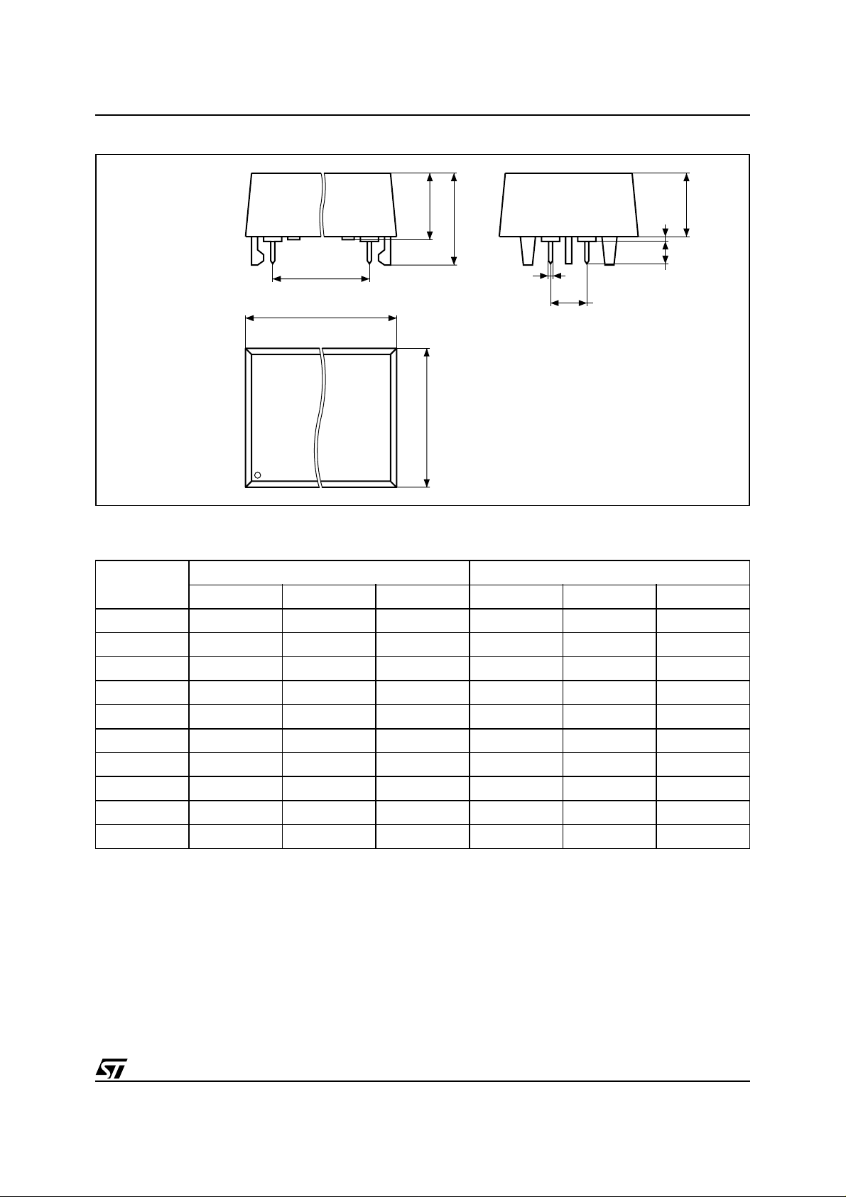
Figure 19. SH – 4-pin SNAPHAT Housing for 48mAh Battery & Crystal, Package Outline
eA
D
A1
A
B
eB
A3
L
E
SHTK-A
Note: Drawing is not to scale.
Table 16. SH – 4-pin SN APHAT Housing for 48mAh Battery & C r ystal, Package M ech. Dat a
Symb
Typ Min Max Typ Min Max
A 9.78 0.385
A1 6.73 7.24 0.265 0.285
mm inches
A2
A2 6.48 6.99 0.255 0.275
A3 0.38 0.015
B 0.46 0.56 0.018 0.022
D 21.21 21.84 0.835 0.860
E 14.22 14.99 0.560 0.590
eA 15.55 15.95 0.612 0.628
eB 3.20 3.61 0.126 0.142
L 2.03 2.29 0.080 0.090
25/29
Page 26
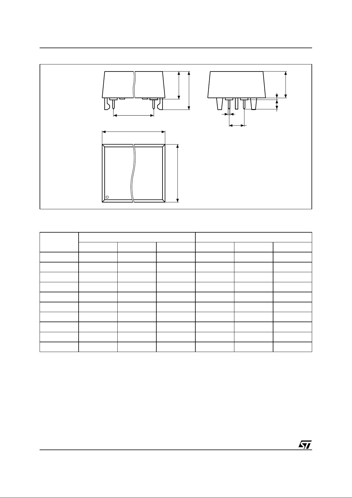
M48T59, M48T59Y, M48T59V*
Figure 20. SH – 4-pin SNAPHAT Housing for 120mAh Battery & Crystal, Package Outline
eA
D
A1
A
B
eB
A3
L
E
SHTK-A
Note: Drawing is not to scale.
Table 17. SH – 4-pin SN APHAT Housing for 120mAh B attery & Crystal, Packag e Mech. Data
Symb
Typ Min Max Typ Min Max
A 10.54 0.415
mm inches
A2
A1 8.00 8.51 0.315 0.335
A2 7.24 8.00 0.285 0.315
A3 0.38 0.015
B 0.46 0.56 0.018 0.022
D 21.21 21.84 0.835 0.860
E 17.27 18.03 0.680 0.710
eA 15.55 15.95 0.612 0.628
eB 3.20 3.61 0.126 0.142
L 2.03 2.29 0.080 0.090
26/29
Page 27
M48T59, M48T59Y, M48T59V*
PART NUMBERING
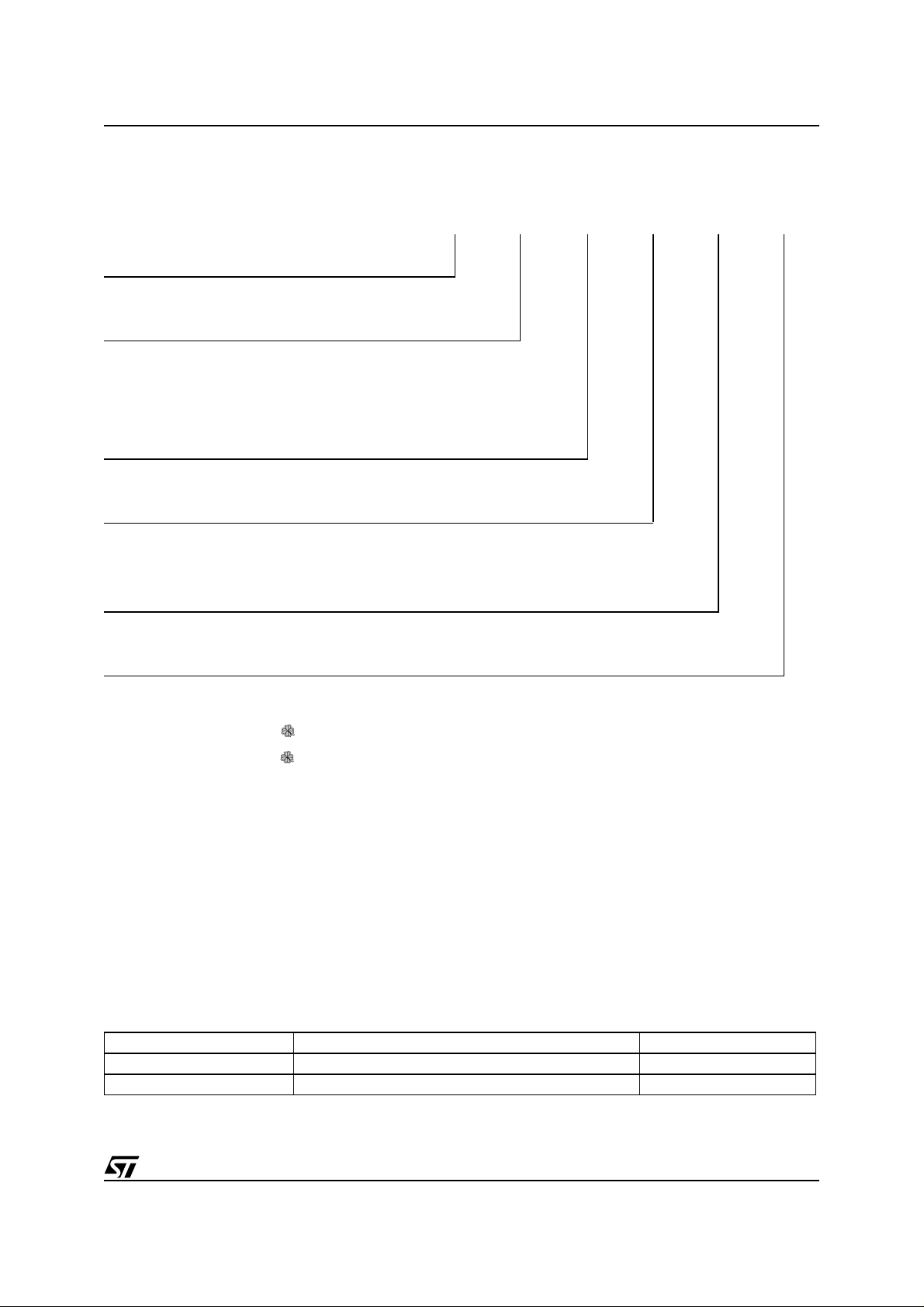
Table 18. Ordering Information Scheme
Example: M48T 59Y –70 MH 1 E
Device Type
M48T
Supply Voltage and Write Protect Voltage
(1)
59
= VCC = 4.75 to 5.5V; V
59Y = V
59V
= 4.5 to 5.5V; V
CC
(2)
= VCC = 3.0 to 3.6V; V
Speed
–70 = 70ns
Package
PC = PCDIP28
(3)
MH
= SOH28
= 4.5 to 4.75V
PFD
= 4.2 to 4.5V
PFD
= 2.7 to 3.0V
PFD
Temperature Range
1 = 0 to 70°C
Shipping Method
For SOH28:
blank = Tubes (Not for New Design - Use E)
E = Lead-free Package (ECO PACK
F = Lead-free Package (ECO PACK
®
), Tubes
®
), Tape & Reel
TR = Tape & Reel (Not for New Design - Use F)
For PCDIP28:
blank = Tubes
Note: 1. The M48T59 part is of fered with t he PCDIP28 (e.g., CAPHAT™) pack age only.
2. Contact local ST sales office for availability of 3.3V version.
3. The S OIC package (SOH28) requires the SNAPHA T
“M4TXX-BR12SH” in plastic tub e or “M4TXX-B R12SHTR” in Ta pe & Reel form (see Table 19).
Caution: Do not place the SNAPHAT battery package “M4TXX-BR12SH” in conductive foam as it will drain the lithium button-cell battery.
®
battery/cry stal packag e whi ch is ordered se parately under the part numbe r
For other options, or for more information on any aspect of this device, please contact the ST Sales Office
nearest you.
Table 19. SNAPHAT Battery Table
Part Number Description Package
M4T28-BR12SH Lithium Battery (48mAh) SNAPHAT SH
M4T32-BR12SH Lithium Battery (120mAh) SNAPHAT SH
27/29
Page 28
M48T59, M48T59Y, M48T59V*
REVISION HISTORY
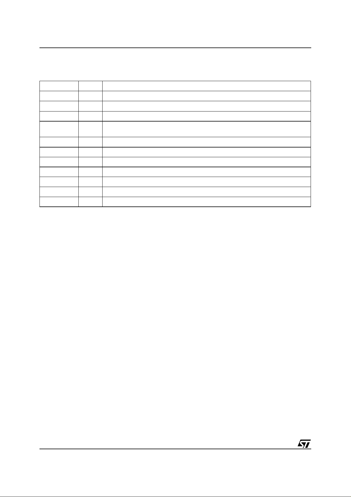
Table 20. Document Revision History
Date Version Revision Details
October 1999 1.0 First Issue
22-Mar-00 1.1
13-Jul-00 2.0 From Preliminary Data to Data Sheet
14-May-01 3.0
31-Jul-01 3.1 Formatting changes from recent document review findings
06-Aug-01 3.2 Fix text for Setting the Alarm Clock (Figure 12)
20-May-02 3.3 Modify reflow time and temperature footnotes (Table 8)
07-Aug-02 3.4 Add marketing status note (Table 18)
01-Apr-03 4.0 v2.2 template applied; test condition updated (Table 13)
02-Apr-04 5.0 Reformatted; update Lead-free package information (Table 8, 18)
25-Nov-04 6.0 Remove all Industrial temperature references (Table 3, 4, 8, 9, 11, 12, 13, 18)
Century Bit Paragraph added; t
Reformatted, Ind. Temp. added (Table 9), SNAPHAT table added (Table 19), temp/voltage
info. added to tables (Table 10, 11, 3, 4, 12, 13)
value changed (Table 12)
FB
28/29
Page 29

M48T59, M48T59Y, M48T59V*
Information furnished is believed to be accurate and reliable. However, STMicroelectronics a ssumes no responsibility fo r the c onsequences
of use of such information nor for any infringement of patents or other rights of third parties which may result from its use. No license is granted
by implication or otherwise under any patent or patent rights of STMicroelectronics. Specifications mentioned in this publication are subject
to change without notice. This publication supersedes and replaces all information previously supplied. STMicroelectronics products are not
authori zed for use as crit i cal compon ent s in life supp ort devices or systems wi thout express written app roval of STMi croelectro nics.
The ST logo is a registered trademark of STMicroel ectronics.
All other nam es are the pro perty of their respective owners
© 2004 STMi croelectro ni cs - All righ ts reserved
Australi a - Belgium - B razil - Canad a - China - Czech Republic - F i nl and - France - Germany - H ong Kong - Ind ia - Is rael - Italy - Japan -
Malaysia - M al ta - Morocco - Singapore - Spain - Swe den - Switze rl and - Unite d K i ngdom - United States of America
STMicroelectron ics group of com panies
www.st.com
29/29
 Loading...