

Page 1
5V, 256 Kbit (32 Kb x8) TIMEKEEPER® SRAM
FEAT URES SUMMARY
■ INTEGRATED, ULT RA LOW POWER SRAM,
REAL TIME CLOCK, POWER-FAIL
CONTROL CIRCUIT AND BATTERY
■ BYTEWIDE™ RAM-LIKE CLOCK ACCESS
■ BCD CODED YEAR, MONTH, DAY, DATE,
HOURS, MINUTES, AND SECONDS
■ FREQUENCY TEST OUTPUT FOR REAL
TIME CLOCK
■ AUTOMATIC POWER-FAIL CHIP
DESELECT AND WRITE PROTECT ION
■ WRITE PROTECT VOLTAGES
= Power-fail Deselect Voltage):
(V
PFD
– M48T35: V
4.5V ≤ V
– M48T35Y: V
4.2V ≤ V
■ SELF-CONTAINED BATTERY AND
CRYSTAL IN THE CAPHAT™ DIP
PACKAGE
■ SOIC PACKAGE PROVIDES DIRECT
CONNECTION FOR A SNAPHAT
HOUSING CONTAINING THE BATTERY
AND CRYSTAL
■ SNAPHAT
®
CRYSTAL) IS REPLACEABLE
■ PIN AND FUNCTION COMPATIBLE WITH
JEDEC STANDARD 32 Kb x 8 SRAMs
= 4.75 to 5.5V
CC
≤ 4.75V
PFD
= 4.5 to 5.5V
CC
≤ 4.5V
PFD
®
HOUSING (BATTERY AND
M48T35
M48T35Y
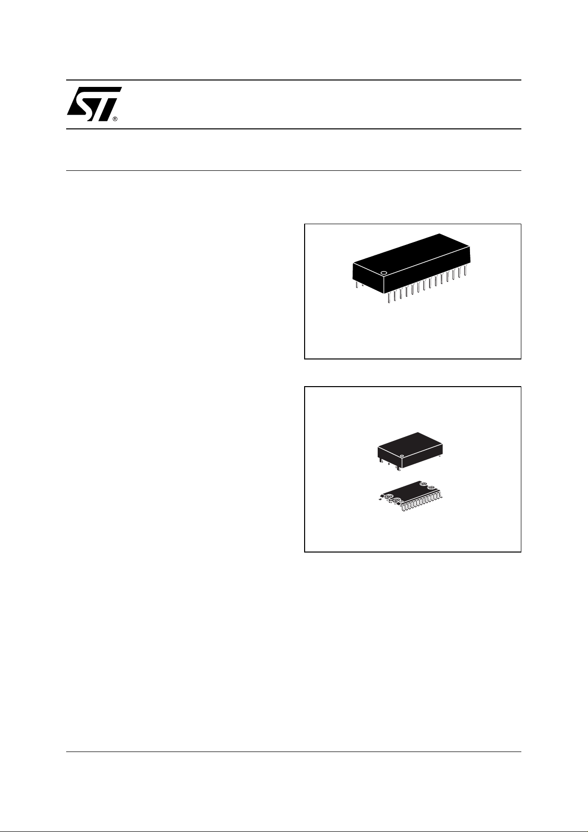
Figure 1. 28-pin PCDIP, CAPHAT™ Package
28
1
PCDIP28 (PC)
Battery/Crystal
CAPHAT
Figure 2. 28-pi n S O I C Package
SNAPHAT (SH)
Battery/Crystal
28
1
SOH28 (MH)
1/26April 2004
Page 2

M48T35, M48T35Y
TABLE OF CONTENTS
FEATURES SUMMARY . . . . . . . . . . . . . . . . . . . . . . . . . . . . . . . . . . . . . . . . . . . . . . . . . . . . . . . . . . . . . 1
Figure 1. 28-pin PCDIP, CAPHAT™ Package . . . . . . . . . . . . . . . . . . . . . . . . . . . . . . . . . . . . . . . . . 1
Figure 2. 28-pin SOIC Package . . . . . . . . . . . . . . . . . . . . . . . . . . . . . . . . . . . . . . . . . . . . . . . . . . . . 1
SUMMARY DESCRIPTION. . . . . . . . . . . . . . . . . . . . . . . . . . . . . . . . . . . . . . . . . . . . . . . . . . . . . . . . . . . 4
Figure 3. Logic Diagram . . . . . . . . . . . . . . . . . . . . . . . . . . . . . . . . . . . . . . . . . . . . . . . . . . . . . . . . . . 4
Table 1. Signal Names . . . . . . . . . . . . . . . . . . . . . . . . . . . . . . . . . . . . . . . . . . . . . . . . . . . . . . . . . . 4
Figure 4. DIP Connections . . . . . . . . . . . . . . . . . . . . . . . . . . . . . . . . . . . . . . . . . . . . . . . . . . . . . . . . 5
Figure 5. SOIC Connections. . . . . . . . . . . . . . . . . . . . . . . . . . . . . . . . . . . . . . . . . . . . . . . . . . . . . . . 5
Figure 6. Block Diagram . . . . . . . . . . . . . . . . . . . . . . . . . . . . . . . . . . . . . . . . . . . . . . . . . . . . . . . . . . 5
OPERATION MODES . . . . . . . . . . . . . . . . . . . . . . . . . . . . . . . . . . . . . . . . . . . . . . . . . . . . . . . . . . . . . . . 6
Table 2. Operating Modes. . . . . . . . . . . . . . . . . . . . . . . . . . . . . . . . . . . . . . . . . . . . . . . . . . . . . . . . 6
READ Mode . . . . . . . . . . . . . . . . . . . . . . . . . . . . . . . . . . . . . . . . . . . . . . . . . . . . . . . . . . . . . . . . . . . 7
Figure 7. READ Mode AC Waveforms . . . . . . . . . . . . . . . . . . . . . . . . . . . . . . . . . . . . . . . . . . . . . . . 7
Table 3. RE A D Mode AC Charac teristics . . . . . . . . . . . . . . . . . . . . . . . . . . . . . . . . . . . . . . . . . . . . 7
WRITE Mode. . . . . . . . . . . . . . . . . . . . . . . . . . . . . . . . . . . . . . . . . . . . . . . . . . . . . . . . . . . . . . . . . . . 8
Figure 8. WRITE Enable Controlled, WRITE AC Waveform. . . . . . . . . . . . . . . . . . . . . . . . . . . . . . . 8
Figure 9. Chip Enable Controlled, WRITE AC Waveforms. . . . . . . . . . . . . . . . . . . . . . . . . . . . . . . . 8
Table 4. WRITE Mode AC Characteristics . . . . . . . . . . . . . . . . . . . . . . . . . . . . . . . . . . . . . . . . . . . 9
Data Retention Mode. . . . . . . . . . . . . . . . . . . . . . . . . . . . . . . . . . . . . . . . . . . . . . . . . . . . . . . . . . . 10
CLOCK OPERATIONS . . . . . . . . . . . . . . . . . . . . . . . . . . . . . . . . . . . . . . . . . . . . . . . . . . . . . . . . . . . . . 11
Reading the Clock. . . . . . . . . . . . . . . . . . . . . . . . . . . . . . . . . . . . . . . . . . . . . . . . . . . . . . . . . . . . . 11
Setting the Clock. . . . . . . . . . . . . . . . . . . . . . . . . . . . . . . . . . . . . . . . . . . . . . . . . . . . . . . . . . . . . . 11
Stopping and Starting the Oscillator. . . . . . . . . . . . . . . . . . . . . . . . . . . . . . . . . . . . . . . . . . . . . . 11
Table 5. Register Map . . . . . . . . . . . . . . . . . . . . . . . . . . . . . . . . . . . . . . . . . . . . . . . . . . . . . . . . . . 11
Calibrating the Clock. . . . . . . . . . . . . . . . . . . . . . . . . . . . . . . . . . . . . . . . . . . . . . . . . . . . . . . . . . . 12
Century Bit. . . . . . . . . . . . . . . . . . . . . . . . . . . . . . . . . . . . . . . . . . . . . . . . . . . . . . . . . . . . . . . . . . . 1 2
Figure 10.Crystal Accuracy Across Temperature . . . . . . . . . . . . . . . . . . . . . . . . . . . . . . . . . . . . . . 13
Figure 11.Clock Calibration. . . . . . . . . . . . . . . . . . . . . . . . . . . . . . . . . . . . . . . . . . . . . . . . . . . . . . . 13
V
Noise And Negative Going Transients. . . . . . . . . . . . . . . . . . . . . . . . . . . . . . . . . . . . . . . . . 14
CC
Figure 12.Supply Voltage Protection. . . . . . . . . . . . . . . . . . . . . . . . . . . . . . . . . . . . . . . . . . . . . . . . 14
MAXIMUM RATING. . . . . . . . . . . . . . . . . . . . . . . . . . . . . . . . . . . . . . . . . . . . . . . . . . . . . . . . . . . . . . . . 15
Table 6. Absolute Maximum Ratings. . . . . . . . . . . . . . . . . . . . . . . . . . . . . . . . . . . . . . . . . . . . . . . 15
DC AND AC PARAMETERS. . . . . . . . . . . . . . . . . . . . . . . . . . . . . . . . . . . . . . . . . . . . . . . . . . . . . . . . . 16
Table 7. Operating and AC Measurement Conditions. . . . . . . . . . . . . . . . . . . . . . . . . . . . . . . . . . 16
Figure 13.AC Measurement Load Circuit . . . . . . . . . . . . . . . . . . . . . . . . . . . . . . . . . . . . . . . . . . . . 16
Table 8. Capacitance . . . . . . . . . . . . . . . . . . . . . . . . . . . . . . . . . . . . . . . . . . . . . . . . . . . . . . . . . . . 1 6
Table 9. DC Characteristics. . . . . . . . . . . . . . . . . . . . . . . . . . . . . . . . . . . . . . . . . . . . . . . . . . . . . . 17
Figure 14.Power Down/Up Mode AC Waveforms. . . . . . . . . . . . . . . . . . . . . . . . . . . . . . . . . . . . . . 18
2/26
Page 3

M48T35, M48T35Y
Table 10.Power Down/Up AC Characteristics . . . . . . . . . . . . . . . . . . . . . . . . . . . . . . . . . . . . . . . . 18
Table 11.Power Down/Up Trip Points DC Characteristics . . . . . . . . . . . . . . . . . . . . . . . . . . . . . . . 18
PACKAGE MECHANICAL INFORMATION . . . . . . . . . . . . . . . . . . . . . . . . . . . . . . . . . . . . . . . . . . . . . 19
Figure 15.PCDIP28 – 28-pin Plastic DIP, battery CAPHAT, Package Outline . . . . . . . . . . . . . . . . 19
Table 12. PCDIP28 – 28-pin Plastic DIP, battery CAPHAT, Package Mechanical Data. . . . . . . . . 19
Figure 16.SOH28 – 28-lead Plastic Small Outline, 4-socket battery SNAPHAT, Package Outline. 20
Table 13. SOH28 – 28-lead Plastic SO, 4-socket battery SNAPHAT, Package Mech. Data . . . . . 20
Figure 17.SH – 4-pin SNAPHAT Housing for 48mAh Battery & Crystal, Package Outline . . . . . . . 21
Table 14. SH – 4-pin SNAPHAT Housing for 48mAh Battery & Crystal, Package Mech. Data. . . . 21
Figure 18.SH – 4-pin SNAPHAT Housing for 120mAh Battery & Crystal, Package Outline . . . . . . 22
Table 15. SH – 4-pin SNAPHAT Housing for 120mAh Battery & Crystal, Package Mech. Data. . . 22
Figure 19.PMDIP28 – 28-pin Plastic DIP, Hybrid, Package Outline . . . . . . . . . . . . . . . . . . . . . . . . 23
Table 16. PMDIP28 – 28-pin Plastic DIP, Hybrid, Package Mechanical Data . . . . . . . . . . . . . . . . . 23
PART NUMBERING . . . . . . . . . . . . . . . . . . . . . . . . . . . . . . . . . . . . . . . . . . . . . . . . . . . . . . . . . . . . . . . 24
Table 17.Ordering Information Scheme . . . . . . . . . . . . . . . . . . . . . . . . . . . . . . . . . . . . . . . . . . . . . 24
Table 18.SNAPHAT Battery Table . . . . . . . . . . . . . . . . . . . . . . . . . . . . . . . . . . . . . . . . . . . . . . . . . 24
REVISION HISTORY. . . . . . . . . . . . . . . . . . . . . . . . . . . . . . . . . . . . . . . . . . . . . . . . . . . . . . . . . . . . . . . 25
Table 19.Document Revision History. . . . . . . . . . . . . . . . . . . . . . . . . . . . . . . . . . . . . . . . . . . . . . . 25
3/26
Page 4
M48T35, M48T35Y
SUMMARY DESCRIPTIO N
The M48T35/Y TIMEKEEPER® RAM is a 32K b x
8 non-volatile static RAM and real time clock. The
monolithic chip is available in two special packages to provide a highly integrated battery backed-up
memory and real time clock solution.
The M48T35/Y is a non-volatile pin and function
equivalent to any JEDEC standard 32Kb x 8
SRAM. It also easily fits into many ROM, EPROM,
and EEPROM sockets, providing the non-volatility
of PROMs without any requirement for special
WRITE timing or limitations on the number of
WRITEs that can be performed.
The 28-pin, 600mil DIP CAPHAT houses the
M48T35/Y silicon with a quartz crystal and a long
life lithium button cell in a single package.
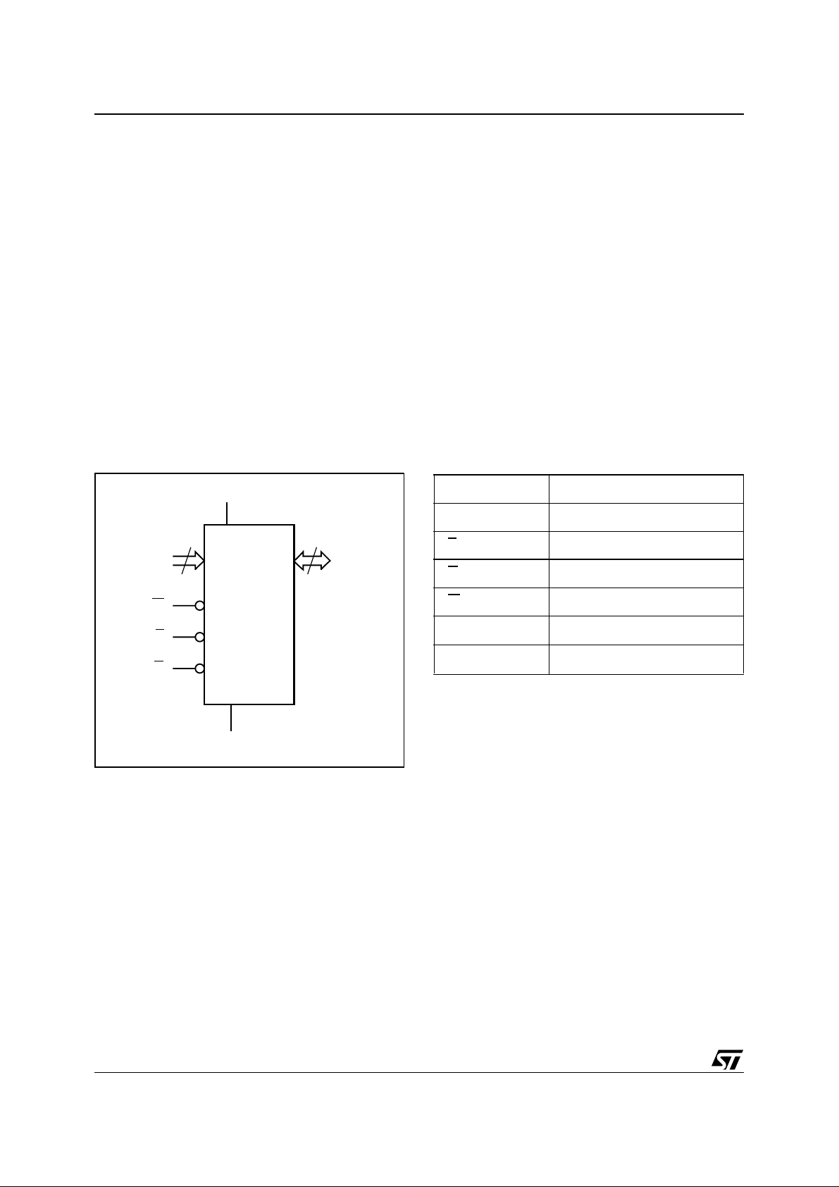
Figure 3. Logic Diagram Table 1. Signal Names
The 28-pin, 330mil SOIC provides sockets with
gold plated contacts at bot h ends for direct connection to a separate SNAPHAT
taining the battery and crystal. The unique design
allows the SNAPHAT battery package to be
mounted on top of the SOIC package after the
completion of the surface mount process. Insertion of the SNAPHAT housing after reflow prevents potential battery and c rystal dam age due to
the high temperatures required for device surfacemounting. The SNAPHAT housing is keyed to prevent reverse insertion. The SOIC and battery/crystal packages are shipped separately in plastic antistatic tubes or in Tape & Reel form.
For the 28-lead SOIC, the battery/crystal package
(e.g., SNAPHAT) part number is “M4T28BR12SH” (see Table 18., page 24).
®
housing con-
A0-A14
W
V
CC
15
M48T35
M48T35Y
E
G
V
SS
8
DQ0-DQ7
AI01620B
A0-A14 Address Inputs
DQ0-DQ7 Data Inputs / Outputs
E
G
W
V
V
CC
SS
Chip Enable
Output Enable
WRITE Enable
Supply Voltage
Ground
4/26
Page 5
M48T35, M48T35Y
Figure 4. DIP C on ne ctions Figure 5. SOI C Co nn e ct io ns
1
A14 V
2
A12
3
A7
4
A6
5
A5
A4
6
A3
7
M48T35
8
A2
A1
A0
DQ0
M48T35Y
9
10
11
12
DQ2
13
14
SS
Figure 6. Block Diagram
28
27
26
25
24
23
22
21
20
19
18
17
16
15
AI01621B
CC
W
A13
A8
A9
A11
G
A10
E
DQ7
DQ6
DQ5DQ1
DQ4
DQ3V
A14 V
A12
A7
A6
A5
A4
A3
A2
A1
A0
DQ0
1
2
3
4
5
6
7
8
9
10
11
M48T35Y
12
DQ2
SS
13
14
AI01622B
28
27
26
25
24
23
22
21
20
19
18
17
16
15
CC
W
A13
A8
A9
A11
G
A10
E
DQ7
DQ6
DQ5DQ1
DQ4
DQ3V
32,768 Hz
CRYSTAL
LITHIUM
CELL
OSCILLATOR AND
CLOCK CHAIN
VOLTAGE SENSE
AND
SWITCHING
CIRCUITRY
V
CC
POWER
V
PFD
8 x 8 BiPORT
SRAM ARRAY
32,760 x 8
SRAM ARRAY
V
SS
A0-A14
DQ0-DQ7
E
W
G
AI01623
5/26
Page 6
M48T35, M48T35Y
OPERATION MODES
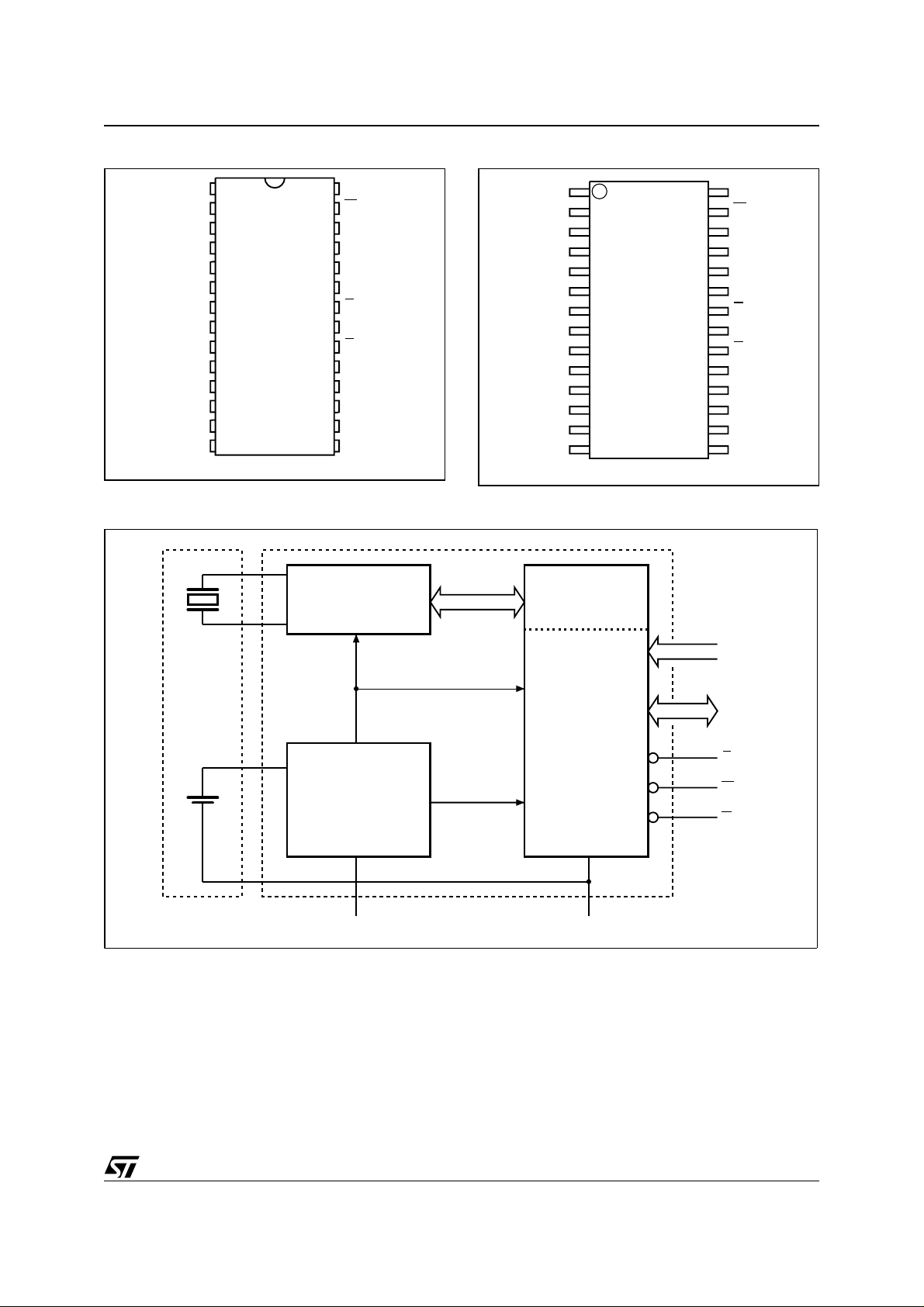
As Figure 6., page 5 shows, the static memory array and the quartz controlled clock oscillator of the
M48T35/Y are integr ated on one silicon c hip. T he
two circuits are interconnected at the up per eight
memory locations to provide user accessible
BYTEWIDE clock information in the bytes with addresses 7FF8h-7FFFh.
The clock locations contain the year, month, date,
day, hour, minute, and second in 24 hour BCD format. Corrections for 28, 29 (leap yea r - valid until
2100), 30, and 31 day months are made automatically. Byte 7FF8h is the clock control register. This
byte controls user access t o the clock inform ation
and also stores the clock calibration setting.
The eight clock bytes are not the actual clock
counters themselves; they are memory locations
consisting of BiPORT™ READ/WRITE memory
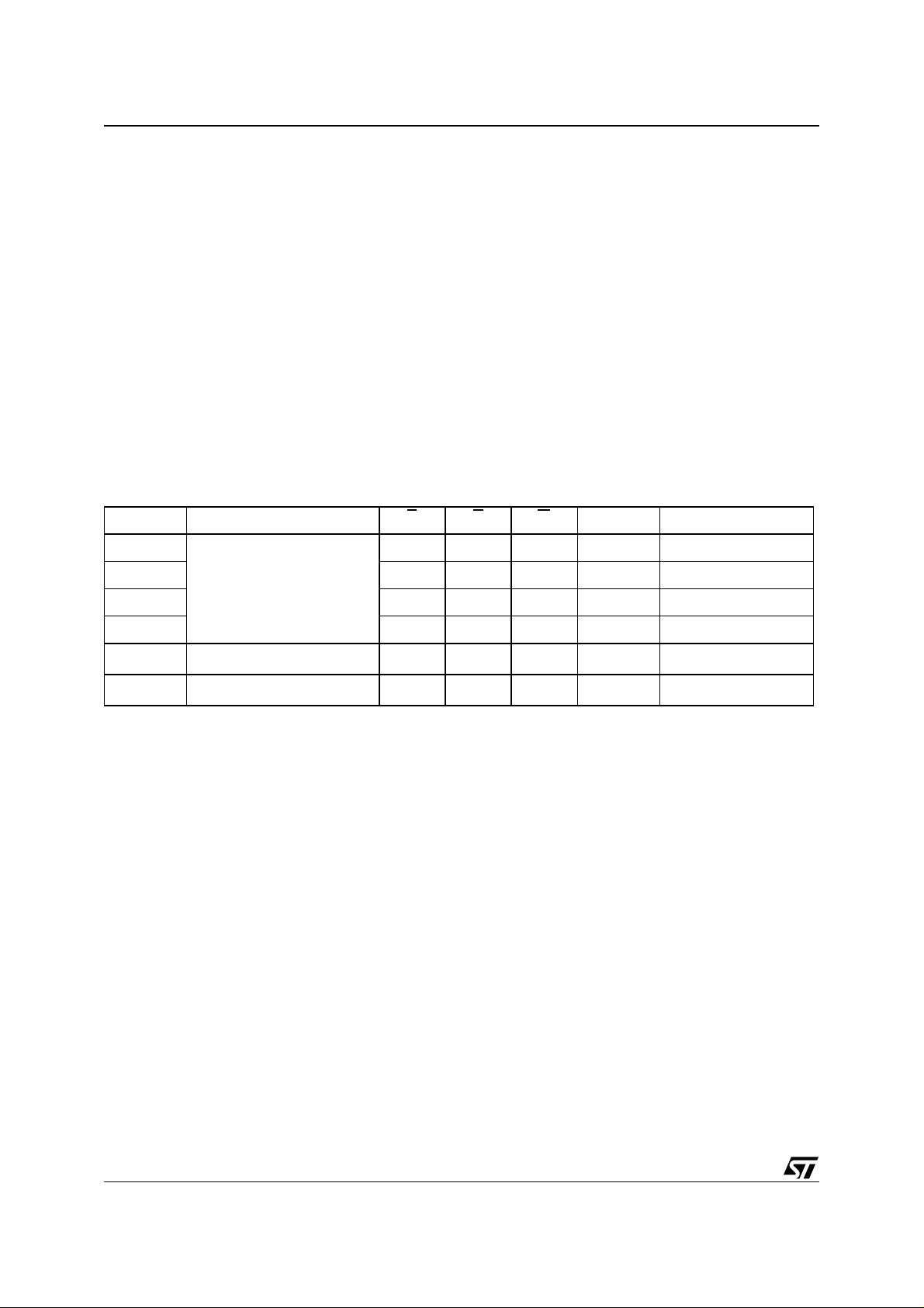
Table 2. Operating Modes
Mode
Deselect
WRITE
READ
READ
Deselect
Deselect
Note: X = VIH or VIL; VSO = Batte ry Back-up Switchover Vo l tage.
1. See Table 11., page 18 for details.
V
V
4.75 to 5.5V
4.5 to 5.5V
to V
SO
PFD
≤ V
or
SO
CC
(min)
(1)
(1)
E G W DQ0-DQ7 Power
V
IH
V
IL
V
IL
V
IL
X X X High Z C MOS Standby
X X X High Z Battery Back-up Mode
cells. The M48T35/Y includes a clock control circuit which updates the clock bytes with current information once per second. The information can
be accessed by the user in the same manner as
any other location in the static memory array.
The M48T35/Y also has its own Pow er-fail Detect
circuit. The control circuitry constantly monitors
the single 5V supply for an out of tolerance condition. When V
is out of tolerance, the circuit write
CC
protects the SRAM, providing a high degree of
data security in the midst of unpredictable system
operation brought on by low V
. As VCC falls be-
CC
low the Battery Back-up Switchover Voltage
), the control circuitry connects the battery
(V
SO
which maintains data and clock operation until valid power returns.
X X High Z Standby
X
V
IL
V
IH
V
IL
V
IH
V
IH
D
IN
D
OUT
High Z Active
Active
Active
6/26
Page 7
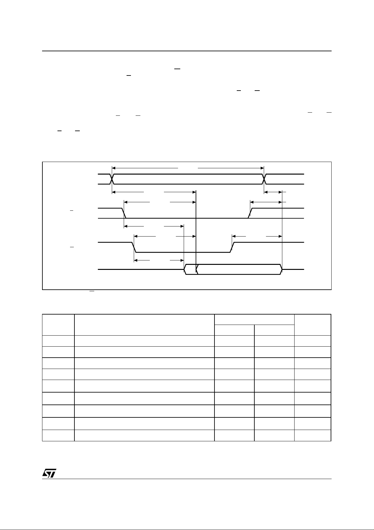
READ Mode
The M48T35/Y is in the READ Mode whenever W
(WRITE Enable) is high and E (Chip Enable) is
low. The unique address specified by the 15 Address Inputs defines which one of the 32,768 bytes
of data is to be acces sed . Vali d data w ill be av ailable at the Data I/O pi ns within Address Access
time (t
stable, providing that the E
) after the last address input signal is
AVQV
and G access times
are also satisfied.
If the E
and G access times are not met, valid data
will be avai la ble after the latter of the Chi p Ena ble
Figure 7. READ Mode AC Waveforms
M48T35, M48T35Y
Access time (t
).
(t
GLQV
The state of the eight t hree-state Da ta I/O si gnals
is controlled by E
ed before t
AVQV
indeterminate state until t
If the Address Inputs are changed while E
remain active, output data will remain valid for Output Data Hold time (t
nate until the next Address Access.
tAVAV
) or Output Enable Access time
ELQV
and G. If the outputs are activat-
, the data lines will be driven to an
.
AVQV
) but will go indetermi-
AXQX
and G
A0-A14
tAVQV tAXQX
tELQV
E
tELQX
tGLQV
G
tGLQX
DQ0-DQ7
Note: W RITE Enable (W) = High.
VALID
tEHQZ
tGHQZ
VALID
AI00925
Table 3. READ Mode AC Characteristics
Symbol
t
AVAV
t
AVQV
t
ELQV
t
GLQV
t
ELQX
t
GLQX
t
EHQZ
t
GHQZ
t
AXQX
Note: 1. Valid for Ambient Op erating Temp erature: TA = 0 to 70 or –40 to 85°C; VCC = 4.75 to 5.5V or 4. 5 to 5.5V (except where noted) .
2. C
READ Cycle Time 70 ns
Address Valid to Output Valid 70 ns
Chip Enable Low to Output Valid 70 ns
Output Enable Low to Output Valid 35 ns
(2)
Chip Enable Low to Output Transition 5 ns
(2)
Output Enable Low to Output Transition 5 ns
(2)
Chip Enable High to Output Hi-Z 25 ns
(2)
Output Enable High to Output Hi-Z 25 ns
Address Transition to Output Transition 10 ns
= 5pF.
L
Parameter
(1)
M48T35/Y
Unit
Min Max
7/26
Page 8
M48T35, M48T35Y
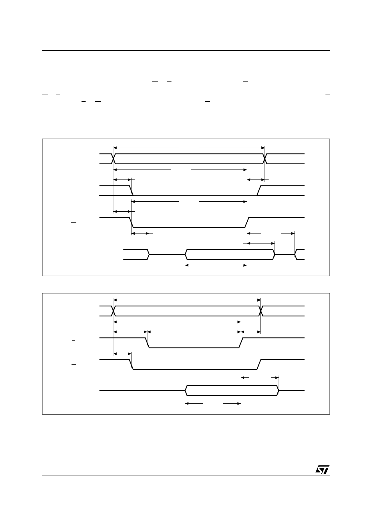
WRITE Mode
The M48T35/Y is in the WRITE Mode whenever W
and E are low. The start of a WRITE is referenced
from the latter occurri ng fallin g edge of W
or E. A
WRITE is terminated by the earlier rising edge of
or E. The addresses must be held valid through-
W
out the cycle. E
mum of t
or W must return high for a mini-
from Chip Enable or t
EHAX
WHAX
from
WRITE Enable prior to the initiation of another
Figure 8. WRITE Enable Controlled, WRITE AC Waveform
READ or WRITE Cycle. Data-in must be valid t
prior to the end of WRITE and remain valid for
VWH
t
WHDX
WRITE Cycles to avoid bu s contention; although,
if the output bus has been activated by a low on E
and G, a low o n W will d isable the out puts t
after W falls.
tAVAV
D-
afterward. G should be kept high during
WLQZ
A0-A14
tAVEL
E
tAVWL
W
tWLQZ
DQ0-DQ7
VALID
tAVWH
tWLWH
Figure 9. Chip Enable Controlled, WRITE AC Waveforms
tAVAV
A0-A14
tAVEL
VALID
tAVEH
tELEH
tDVWH
tWHAX
tWHQX
tWHDX
DATA INPUT
AI00926
tEHAX
8/26
E
W
DQ0-DQ7
tAVWL
DATA INPUT
tDVEH
tEHDX
AI00927
Page 9
M48T35, M48T35Y
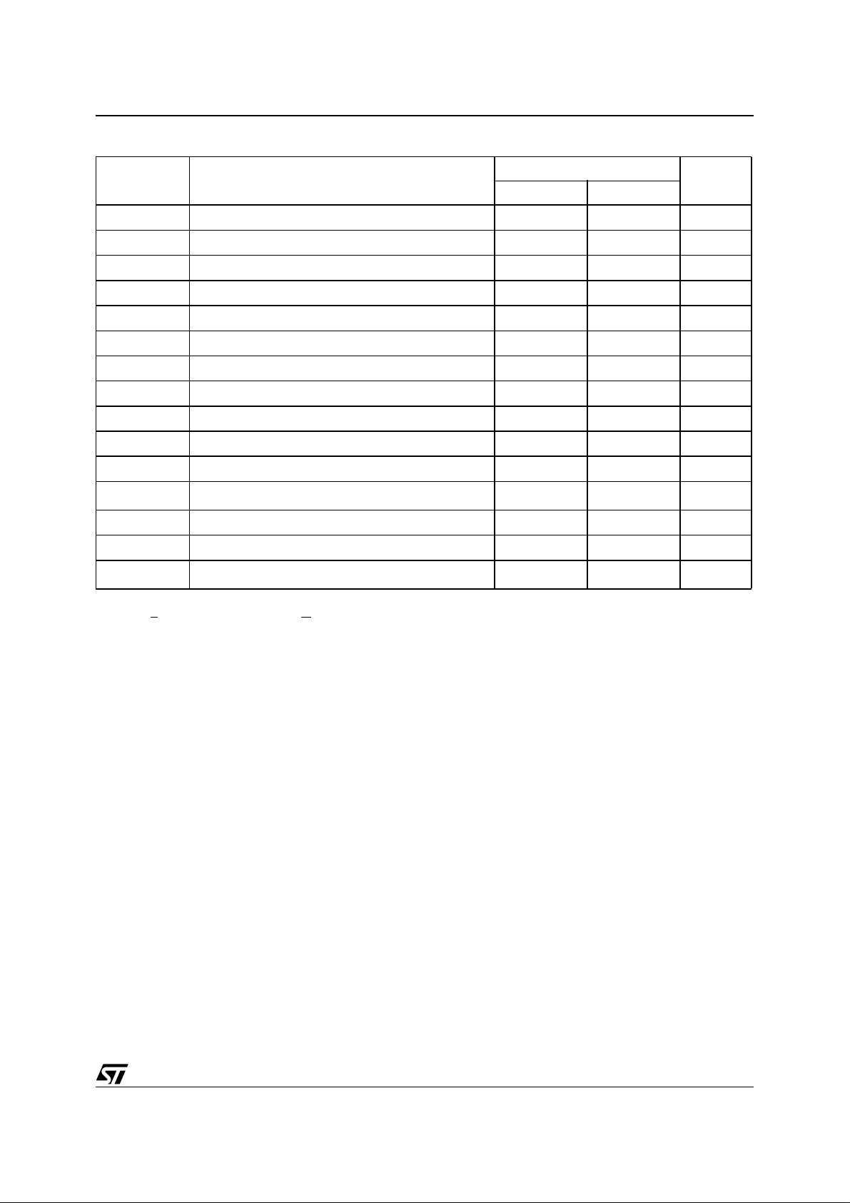
Table 4. WRITE Mode AC Characteristics
Symbol
t
AVAV
t
AVWL
t
AVEL
t
WLWH
t
ELEH
t
WHAX
t
EHAX
t
DVWH
t
DVEH
t
WHDX
t
EHDX
(2,3)
t
WLQZ
t
AVWH
t
AVEH
(2,3)
t
WHQX
Note: 1. Valid for Ambient Op erating Temp erature: TA = 0 to 70 or –40 to 85°C; VCC = 4.75 to 5.5V or 4. 5 to 5.5V (except where noted) .
2. C
L
3. If E
WRITE Cycle Time 70 ns
Address Valid to WRITE Enable Low 0 ns
Address Valid to Chip Enable Low 0 ns
WRITE Enable Pulse Width 50 ns
Chip Enable Low to Chip Enable High 55 ns
WRITE Enable High to Address Transition 0 ns
Chip Enable High to Address Transition 0 ns
Input Valid to WRITE Enable High 30 ns
Input Valid to Chip Enable High 30 ns
WRITE Enable High to Input Transition 5 ns
Chip Enable High to Input Transition 5 ns
WRITE Enable Low to Output Hi-Z 25 ns
Address Valid to WRITE Enable High 60 ns
Address Valid to Chip Enable High 60 ns
WRITE Enable High to Output Transition 5 ns
= 5pF.
goes low simultaneously with W going low, the outp uts remain in the high impeda nce state.
Parameter
(1)
M48T35/Y
Unit
Min Max
9/26
Page 10

M48T35, M48T35Y
Data Retention Mode
With valid V
a conventional BYTEWIDE static RAM. Should
the supply volt age decay, the RA M will a utomatically power-fail deselect, write protecting itself
when V
window. All outputs become high impedance, and
all inputs are treated as “Don't care” (see Figure
14., page 18, Table 10., page 18, and Table
11., page 18).
Note: A power failure during a WRITE cycle may
corrupt data at the currently a ddressed location,
but does not jeopardize the rest of the RAM's content. At voltages below V
assured the memory will be i n a write protected
state, provided the V
The M48T35/Y may respond to transient noise
spikes on V
during the time the device is sampling V
applied, the M48T35/Y operates as
CC
falls w ithin the V
CC
PFD
fall time is not less than tF.
CC
that reach into the deselect window
CC
(max), V
PFD
(min), the user can be
PFD
. There-
CC
(min)
fore, decoupling of t he power supply l ines is recommended.
When V
drops below VSO, the control circuit
CC
switches power to the internal battery which preserves data and powers the clock. The internal
button cell will maintain data in the M48T35/Y for
an accumulated period of at least 7 years when
is less than VSO. As system power returns
V
CC
and V
rises above VSO, the battery is disc on-
CC
nected, and the power supply is switched to external V
reaches V
kept high as V
. Write protection continues until V
CC
(min) plus t
PFD
rises past V
CC
(min). E should be
rec
(min) to prevent
PFD
CC
inadvertent WRITE Cycles prior to p rocessor stabilization. Normal RAM operation can resume t
after VCC exceeds V
PFD
(max).
rec
For more information on Battery Storage Life refer
to the Application Note AN1012.
10/26
Page 11
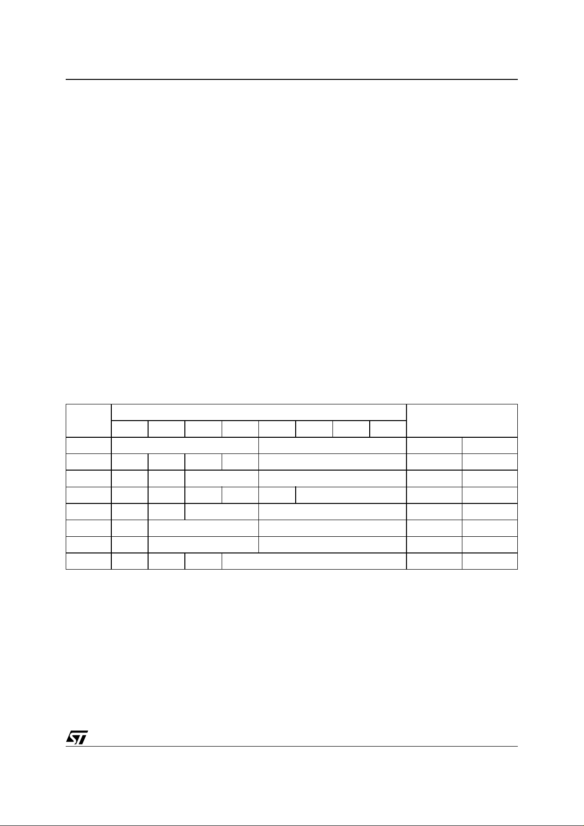
CLOCK OPERATIONS
Reading the Clock
Updates to the TIMEKEEPER
ble 5) should be halted before clock data is read to
prevent reading data in transition. The BiPORT™
TIMEKEEPER cells in the RAM array are only
data registers and not the actual clock c ounters,
so updating the registers can be halted without
disturbing the clock itself.
Updating is halted when a '1' is written to the
READ Bit, D6 in the Control Register 7FF8h. As
long as a '1' remains in that position , updating is
halted.
After a halt is issued, the registers reflect the
count; that is, the day, date, and the time that were
current at the moment the halt command was issued.
All of the TIMEKEEPER registers are updated simultaneously. A halt will not interrupt an update in
progress. Updating is within a second after the bit
is reset to a '0.'
Setting the Clock
Bit D7 of the Control Register 7FF8h is the WRITE
Bit. Setting the WRITE Bit to a '1,' like the REA D
Bit, halts updates to the TIMEKEEPER
®
registers (see Ta-
®
registers.
M48T35, M48T35Y
The user can then load them with the correct day,
date, and time data in 24 hour BCD f ormat (see
Table 5). Resetting the WRITE Bit to a '0' then
transfers the values of all time registers 7FF9h7FFFh to the actual TIMEKEEPER counters and
allows normal operation to resume. The FT Bit and
the bits marked as '0' in Table 5 must be written to
'0' to all ow for nor mal TIMEKE EPER and RAM operation. After the WRITE Bit is reset, the next clock
update will occur within one second.
See the Application Note AN923, “TIMEKEEPER
Rolling Into the 21st Century” for information on
Century Rollover.
Stopping and Starting the Oscillator
The oscillator may be stopped at any time. If the
device is going to spend a significant amount of
time on the shelf, the oscillator can be turned off to
minimize current drain on the battery. The STOP
Bit is the MSB of the seconds register. Setting it to
a '1' stops the oscillator. The M48T35/Y is shipped
from STMicroelectronics with t he STOP Bit set to
a '1.' When reset to a '0,' the M48T35/ Y osc illator
starts within 1 second.
®
Table 5. Register Map
Address
D7 D6 D5 D4 D3 D2 D1 D0
7FFFh 10 Years Year Year 00-99
7FFEh 0 0 0 10 M. Month Month 01-12
7FFDh 0 0 10 Date Date Date 01-31
7FFCh 0 FT CEB CB 0 Day Century/Day 00-01/01-07
7FFBh 0 0 10 Hours Hours Hours 00-23
7FFAh 0 10 Minutes Minutes Minutes 00-59
7FF9h ST 10 Seconds Seconds Seconds 00-59
7FF8h W R S Calibration Control
Keys : S = SIGN Bit
FT = FREQUE NCY TEST Bit (Must be set to '0' upon power
for normal operation)
R = READ Bit
W = WRITE B i t
Note: When CEB is set to '1,' CB will toggle from '0' to '1' or from '1' to '0' at the turn of the century (dependent upon the initial value set).
When CEB is set to '0,' CB will not toggle. The WRITE Bit does not need to be set to write to CEB.
Data
ST = STOP Bit
0 = Must be set to '0'
CEB = Centur y E nable Bit
CB = Centur y B i t
Function/Range
BCD Format
11/26
Page 12

M48T35, M48T35Y
Calibrating the Clock
The M48T35/Y is driven by a quartz-controlled oscillator with a nominal frequency of 32,768 Hz. The
devices are tested not to exceed 35 ppm (parts per
million) osci llator frequency error at 25°C, w hich
equates to about ±1.53 minu tes per month. With
the calibration bits properly set, the accuracy of
each M48T35/Y improves to better than +1/–2
ppm at 25°C.
The oscillation rate of any crystal changes with
temperature (see Figure 10., page 13). Most clock
chips compensate for crystal frequency and temperature shift error with cumbersome “trim” capacitors. The M48T35/Y design, however, employs
periodic counter correction. The calibration circuit
adds or subtracts counts from the oscillator divider
circuit at the divide by 256 stage, as shown in Fig-
ure 11., page 13. The num ber of time s pulses are
blanked (subtracted, negat ive calibration) or split
(added, positive calibration) depends upon the
value loaded into the five calibration bits found in
the Control Register. Adding counts speeds the
clock up, subtracting counts slows the clock down.
The Calibration Byte occupies the five lower order
bits (D4-D0) in the Control Register 7FF8h. These
bits can be set to represent any value between 0
and 31 in binary form. Bit D5 is the Sign Bit; '1' indicates positive calibration, '0' indicates negat ive
calibration. Calibration occurs within a 64 m inute
cycle. The first 62 m inut es i n t he c ycle m ay , once
per minute, have one second either shortened by
128 or lengthened by 256 oscillator cycles. If a binary '1' is loaded into the register, only the first 2
minutes in the 64 minute cycle will be modified; if
a binary 6 is loaded, the first 12 will be affected,
and so on.
Therefore, each calibration step has t he effect of
adding 512 or subtracting 256 oscillator cycles for
every 125,829,120 actual oscillator cycles, that is
+4.068 or –2.034 ppm of adjustment per calibration step in the calibrat ion registe r. Assum ing that
the oscillator is in fact running at exactly 32,768
Hz, each of the 31 increm ents in the Calibration
Byte would represent +10.7 or –5. 35 se conds per
month which corresponds to a total range of +5.5
or –2.75 minutes per month.
Two methods are available for ascertaining how
much calibration a given M48T35/Y may require.
The first involves simply setting the clock, letting it
run for a month and comparing it to a known accurate reference (like WWV broadcasts). While that
may seem crude, it allows the designer to give the
end user the ability to calibrate his clock as his environment may require, even after the final product
is packaged in a non-user serviceable enclosure.
All the designer has to do is provide a simple utility
that accesses the Calibration Byte.
The second approach is better suited t o a manufacturing environment, and involves the use of
some test equipment. When the F requency Test
(FT) Bit, the seventh-most significant bit in t he Day
Register is set to a '1,' and D7 of the Seconds Register is a '0' (Oscillator Running), DQ0 will toggle at
512 Hz during a READ of the Seconds Register.
Any deviation from 512 Hz indicates the degree
and direction of oscillator frequency shift at the test
temperature. For example, a reading of 512.01024
Hz would indicate a +20 ppm oscillator frequency
error, requiring a –10 (WR001010) to be loaded
into the Calibration Byte for correction.
Note: Setting or changing the Calibration Byte
does not affect the Frequency Test output frequency.
The FT Bit MUST be reset to '0' for normal clock
operations to resume. The FT Bit is aut omatically
Reset on power-down.
For more information on c alibration, see Application Note AN934, “TIMEKEEPER
®
Calibration.”
Century Bit
Bit D5 and D4 of Clock Register 1FFCh contain
the CENTURY ENABLE Bit (CEB) and the CENTURY Bit (CB). Setting CEB to a '1' will cause CB
to toggle, either from a '0' to '1' or from '1' to '0' at
the turn of the century (depending upon its initial
state). If CEB is set to a '0,' CB will not toggle.
Note: The WRITE Bit must be set in order to write
to the CENTURY Bit.
12/26
Page 13
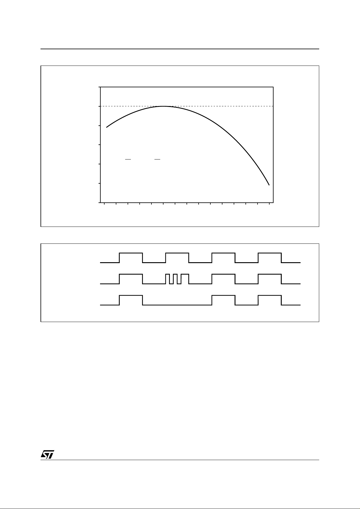
Figure 10. Crystal Accuracy Across Temp eratur e
ppm
20
0
-20
-40
M48T35, M48T35Y
-60
-80
-100
0 5 10 15 20 25 30 35 40 45 50 55 60 65 70
Figure 11. Cl ock Ca l ib rat i on
NORMAL
POSITIVE
CALIBRATION
NEGATIVE
CALIBRATION
∆F
= -0.038 (T - T
F
ppm
T0 = 25 °C
)2 ± 10%
0
2
C
°C
AI02124
AI00594B
13/26
Page 14
M48T35, M48T35Y
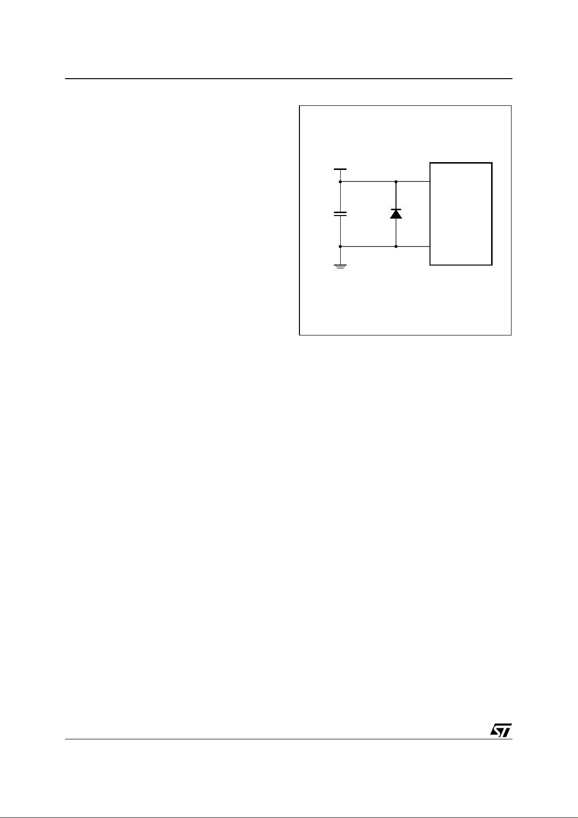
VCC Noise And Negative Going Transients
transients, including those produced by output
I
CC
switching, can produce voltage fluctuations, resulting in spikes on the V
bus. These transients
CC
can be reduced if capacitors are used to store energy which stabilizes the V
bus. The energy
CC
stored in the bypass capacitors will be released as
low going spikes are generated or energy will be
absorbed when overshoots occur. A bypass capacitor value of 0.1µ F (as shown in Figure 12) is
recommended in order to provide the needed filtering.
In addition to transients that are caused by normal
SRAM operation, power cycling can generate negative voltage spikes on V
below V
by as much as one volt. These negative
SS
that drive it to values
CC
spikes can cause data corruption in the SRAM
while in battery backup mode. To protect from
these voltage spikes, it is recommended to connect a schottky diode from V
connected to V
, anode to VSS). Schottky diode
CC
to VSS (cathode
CC
1N5817 is recommended for through hole and
MBRS120T3 is recommended for surface mount.
Figure 12. Supply Voltage Protection
V
CC
V
CC
0.1µF DEVICE
V
SS
AI02169
14/26
Page 15
M48T35, M48T35Y
MAXIMUM RA T ING
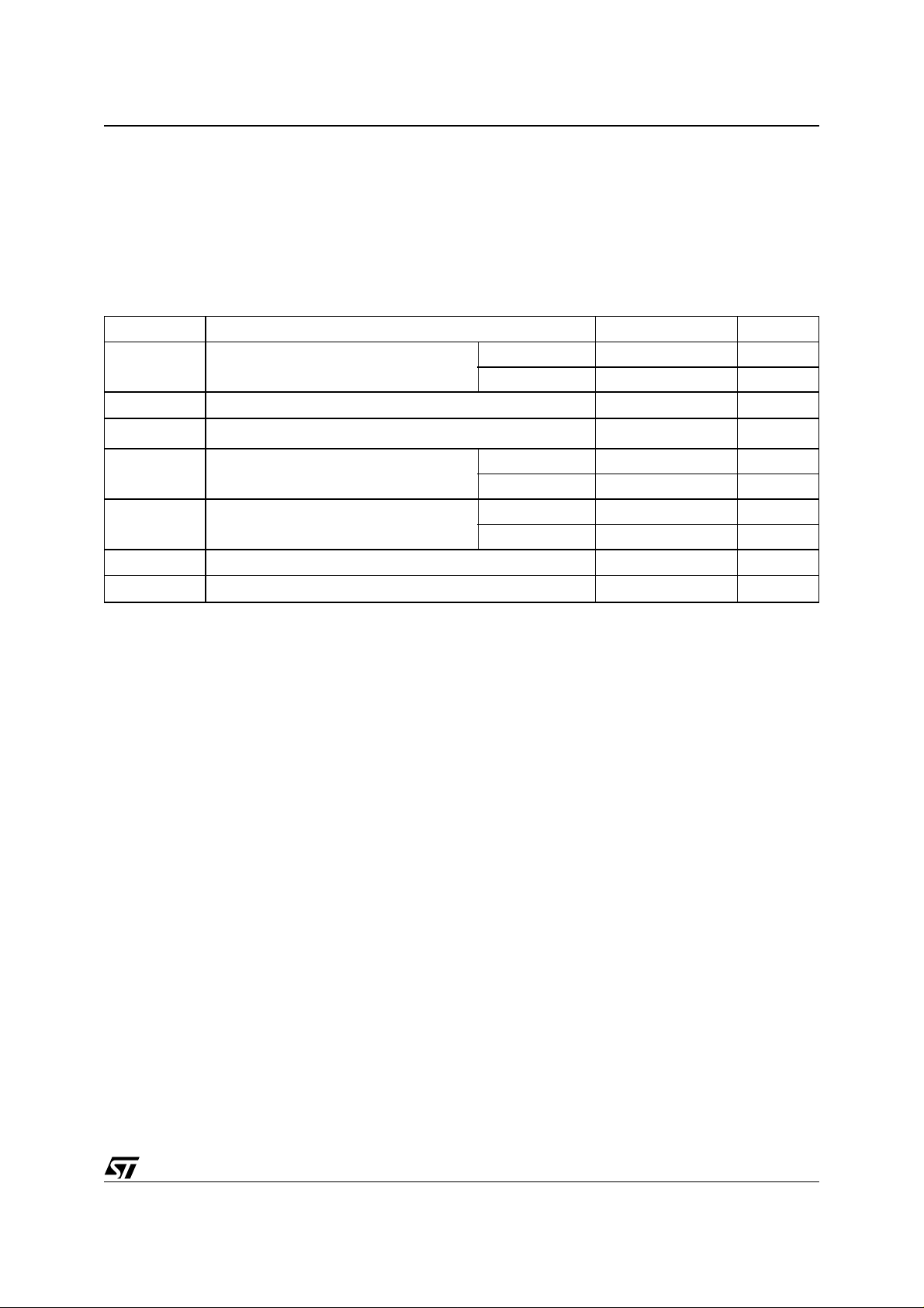
Stressing the device above the rating listed in the
“Absolute Maximum Ratings” table may cause
permanent damage to the device. These are
stress ratings only and operation of the device at
these or any other conditions above those indicated in the Operating sections of this specification is
Table 6. Absolute Maximum Ratings
Symbol Parameter Value Unit
T
A
T
STG
(1,2,3)
T
SLD
V
IO
V
CC
I
O
P
D
Note: 1. For DIP package: Soldering temperature not to exceed 260°C for 10 seconds (total thermal budget not to exceed 150°C for longer
than 30 seconds).
2. For S O package, standard (SnPb) lead finish: Reflow at peak t em perature of 2 25°C (total thermal budget not to excee d 180°C for
between 90 to 15 0 s e c o nds).
3. For S O package , Lead-free (Pb-free) lead finish: Reflow at peak tempera ture of 260°C (total therm al budget n ot to exceed 245°C
for greater than 30 seconds).
CAUTION: Nega tive undershoot s below –0.3V are not allowed on any pin whil e i n the Battery Ba ck-up mode.
CAUTION: Do NOT wave s older SOIC t o avoid dam aging SNAPHAT socket s.
Ambient Operating Temperature
Storage Temperature (VCC Off, Oscillator Off)
Lead Solder Temperature for 10 seconds 260 °C
Input or Output Voltages
Supply Voltage
Output Current 20 mA
Power Dissipation 1 W
not implied. Exposure to Absol ute Max imum Ra ting conditions for extended periods may affect device reliability. Refer also to the
STMicroelectronics SURE Program and other relevant quality documents.
Grade 1 0 to 70 °C
Grade 6 –40 to 85 °C
–40 to 85 °C
M48T35 –0.3 to 7 V
M48T35Y –0.3 to 7 V
M48T35 –0.3 to 7 V
M48T35Y –0.3 to 7 V
15/26
Page 16
M48T35, M48T35Y
DC AND AC PARAMETERS
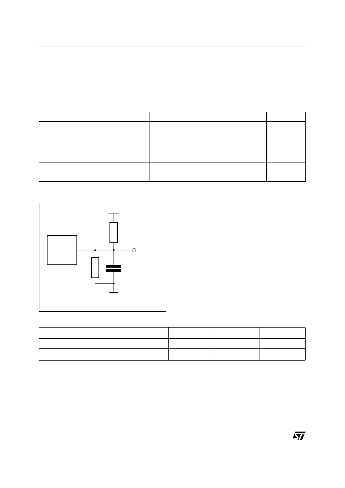
This section summarizes the operating and measurement conditions, as well as the DC and AC
characteristics of the device. The parameters in
the following DC and AC Characteristic tables are
derived from tests performed under the Meas ure-
Table 7. Operating and AC Measurement Conditions
Parameter M48T35 M48T35Y Unit
ment Conditions listed in t he relevant tables. Designers should check that the operating conditions
in their projects match the measurement conditions when using the quoted parameters.
Supply Voltage (V
Ambient Operating Temperature (T
Load Capacitance (C
CC
)
)
A
)
L
4.75 to 5.5 4.5 to 5.5 V
0 to 70 –40 to 85 °C
100 100 pF
Input Rise and Fall Times ≤ 5 ≤ 5ns
Input Pulse Voltages 0 to 3 0 to 3 V
Input and Output Timing Ref. Voltages 1.5 1.5 V
Note: O utput Hi-Z is def i ned as the poin t where data is no l onger driven.
Figure 13. AC Measurement Lo a d Circuit
5V
1.9kΩ
DEVICE
UNDER
TEST
1kΩ
OUT
CL = 100pF or 5pF
CL includes JIG capacitance
AI01030
Table 8. Capacitance
Symbol
C
IN
(3)
C
OUT
Note: 1. Effec tive capacitance measured with powe r supply at 5V; sampled only, not 100% tested.
2. At 25°C, f = 1MHz.
3. Outputs deselect ed.
Input Capacitance 10 pF
Output Capacitance 10 pF
Parameter
16/26
(1,2)
Min Max Unit
Page 17
M48T35, M48T35Y
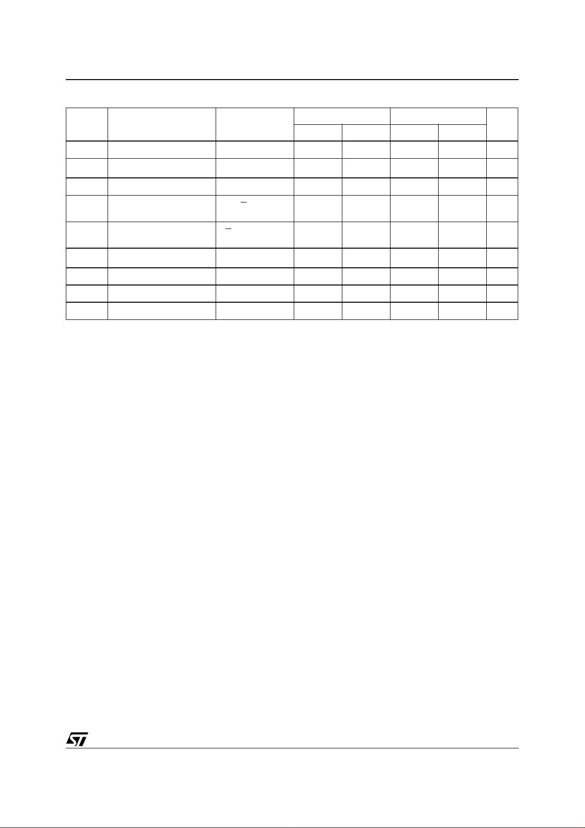
Table 9. DC Characteristics
M48T35 M48T35Y
Unit
MinMaxMinMax
±1 ±1 µA
±1 ±1 µA
33mA
22mA
V
CC
+ 0.3
2.2
VCC + 0.3
0.4 0.4 V
2.4 2.4 V
V
IN
≤ V
≤ V
IH
(1)
CC
CC
Symbol Parameter
I
Input Leakage Curren t
LI
(2)
I
LO
I
I
CC1
I
CC2
V
V
V
V
Note: 1. Valid for Ambient Op erating Temp erature: TA = 0 to 70 or –40 to 85°C; VCC = 4.75 to 5.5V or 4. 5 to 5.5V (except where noted) .
Output Leakage Current
Supply Current Outputs open 50 30 mA
CC
Supply Current (Standby)
TTL
Supply Current (Standby)
CMOS
(3)
Input Low Voltage –0.3 0.8 –0 .3 0.8 V
IL
Input High Voltage 2.2
IH
Output Low Voltage
OL
Output High Voltage
OH
2. Outputs deselect ed.
3. Nega ti ve spike s of –1 V al l owed for up t o 10 ns once per Cy cl e.
Test Condition
0V ≤ V
0V ≤ V
OUT
= V
E
= VCC – 0.2V
E
I
= 2.1mA
OL
I
= –1mA
OH
17/26
Page 18
M48T35, M48T35Y
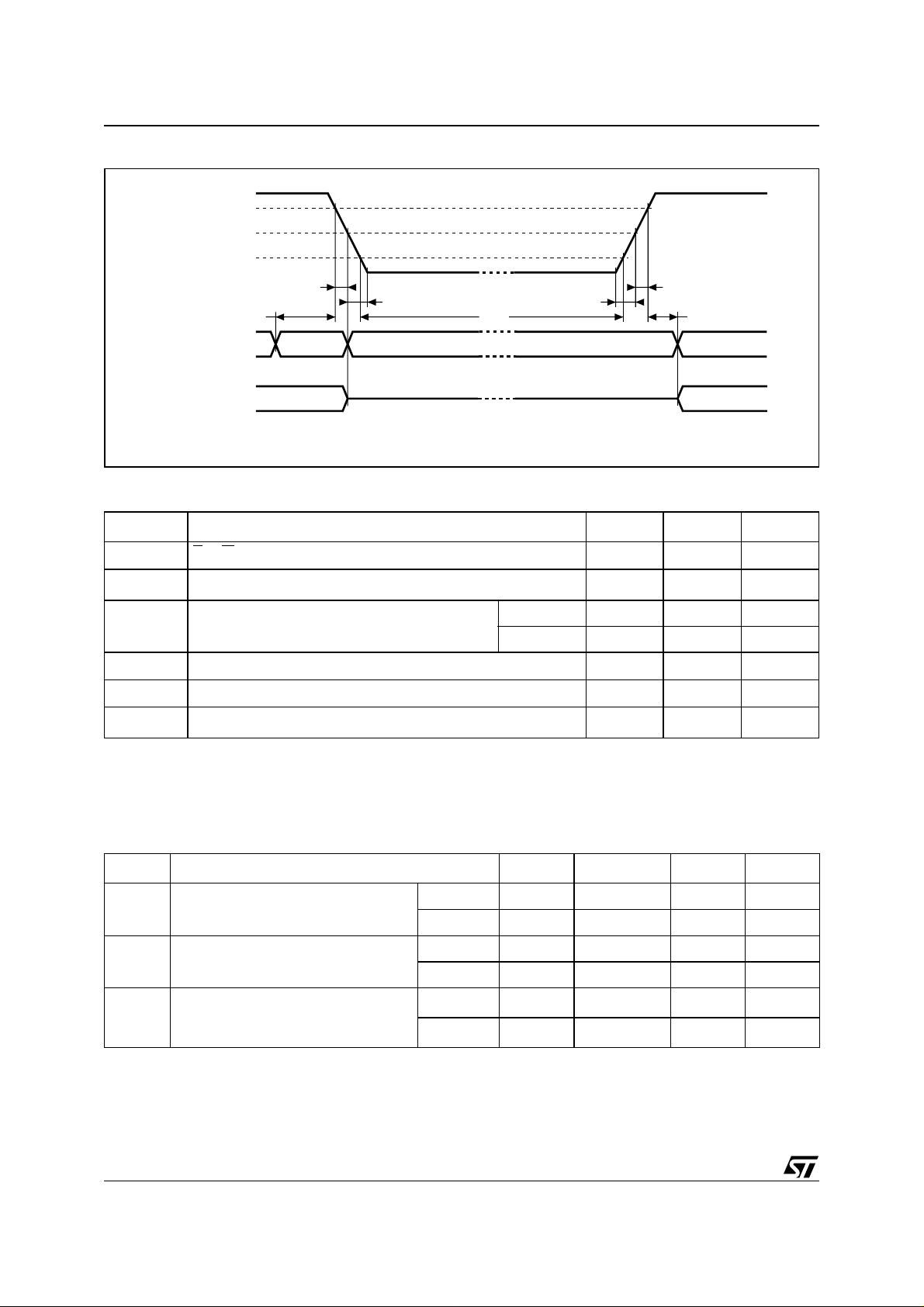
Figure 14. Power Down/Up Mode AC Waveforms
V
CC
V
(max)
PFD
V
(min)
PFD
VSO
INPUTS
OUTPUTS
tF
tPD
VALID VALID
(PER CONTROL INPUT)
tFB
tDR
tRB
DON'T CARE
HIGH-Z
tR
trec
RECOGNIZEDRECOGNIZED
(PER CONTROL INPUT)
AI01168C
Table 10. Power Down/Up AC Characteristics
Symbol
t
PD
(2)
t
F
t
FB
t
R
t
RB
t
rec
Note: 1. Valid for Ambient Op erating Temp erature: TA = 0 to 70 or –40 to 85°C; VCC = 4.75 to 5.5V or 4. 5 to 5.5V (except where noted) .
2. V
3. V
4. t
E or W at VIH before Power Down
V
(max) to V
PFD
(3)
V
(min) to VSS VCC Fall Time
PFD
V
(min) to V
PFD
VSS to V
(4)
V
(max) to Inputs Recognized
PFD
(max) to V
PFD
es V
PFD
(min) to VSS fall time of less than tFB may cause corruption of RA M data.
PFD
(min) = 20ms for industrial temperature Grade 6 device.
rec
(min).
PFD
PFD
PFD
(min) VCC Rise Time
PFD
(min) fall time of less than tF may result in deselection/write protection not occurring until 200µs after VCC pass-
Parameter
(min) VCC Fall Time
(max) VCC Rise Time
(1)
Min Max Unit
0µs
300 µs
M48T35 10 µs
M48T35Y 10 µs
10 µs
1µs
40 200 ms
Table 11. Power Down/Up Trip Points DC Characteristics
Symbol
Parameter
(1,2)
M48T35 4.5 4.6 4.75 V
V
V
t
DR
Note: 1. Valid for Ambient Op erating Temp erature: TA = 0 to 70 or –40 to 85°C; VCC = 4.75 to 5.5V or 4. 5 to 5.5V (except where noted) .
Power-fail Deselect Voltage
PFD
M48T35Y 4.2 4.35 4.5 V
M48T35 3.0 V
Battery Back-up Switchover Voltage
SO
(5)
Expected Data Retention Time
M48T35Y 3.0 V
Grade 1
Grade 6
2. All voltages referenced to V
3. CAPHAT and M4T32-BR12SH1 SNAPHAT only, M4T28-BR12SH1 SNAPHAT top t
4. Us i ng l arger M4T32-BR12SH6 SNA PHAT top (rec om m ended for Industrial Tem perature Range - Grade 6 devic e).
5. At 25°C, V
CC
= 0V.
SS
.
18/26
Min Typ Max Unit
10
10
(3)
(4)
= 7 years (typ).
DR
YEARS
YEARS
Page 19
PACKAG E MECHANICA L INFORMATION
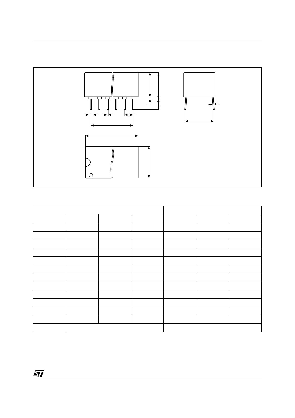
Figure 15. PCDIP28 – 28-pin Plastic DIP, battery CAPHAT, Package Outline
A2
M48T35, M48T35Y
B1 B
A1AL
e1
C
eA
e3
D
N
E
1
Note: D rawing is not to scale.
PCDIP
Table 12. PCDIP28 – 28-pin Plastic DIP, battery CAPHAT, Package Mechanical Data
Symb
Typ Min Max Typ Min Max
A 8.89 9.65 0.350 0.380
A1 0.38 0.76 0.015 0.030
A2 8.38 8.89 0.330 0.350
B 0.38 0.53 0.015 0.021
B1 1.14 1.78 0.045 0.070
mm inches
C 0.20 0.31 0.008 0.012
D 39.37 39.88 1.550 1.570
E 17.83 18.34 0.702 0.722
e1 2.29 2.79 0.090 0.110
e3 29.72 36.32 1.170 1.430
eA 15.24 16.00 0.600 0.630
L 3.05 3.81 0.120 0.150
N 28 28
19/26
Page 20
M48T35, M48T35Y
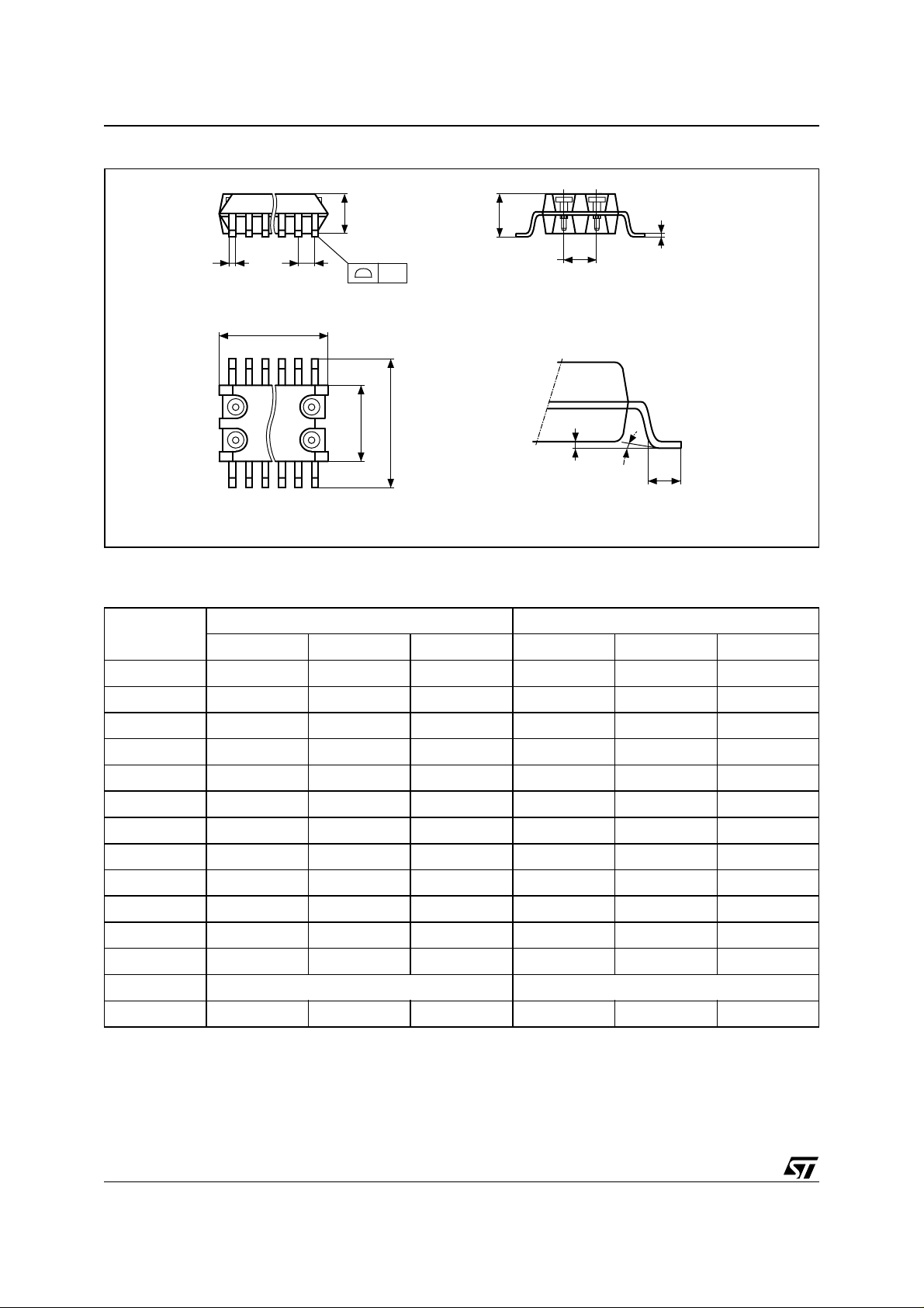
Figure 16. SOH28 – 28-lead Plastic Small Outline, 4-socket battery SNAPHAT, Package Outline
A2
A
C
Be
eB
CP
D
N
E
H
LA1 α
1
SOH-A
Note: D rawing is not to scale.
Table 13. SOH28 – 28-lead Plastic SO, 4-socket battery SNAPHAT, Package Mech. Data
Symb
Typ Min Max Typ Min Max
mm inches
A 3.05 0.120
A1 0.05 0.36 0.002 0.014
A2 2.34 2.69 0.092 0.106
B 0.36 0.51 0.014 0.020
C 0.15 0.32 0.006 0.012
D 17.71 18.49 0.697 0.728
E 8.23 8.89 0.324 0.350
e1.27– –0.050– –
eB 3.20 3.61 0.126 0.142
H 11.51 12.70 0.453 0.500
L 0.41 1.27 0.016 0.050
α 0° 8° 0° 8°
N 28 28
CP 0.10 0.004
20/26
Page 21
M48T35, M48T35Y
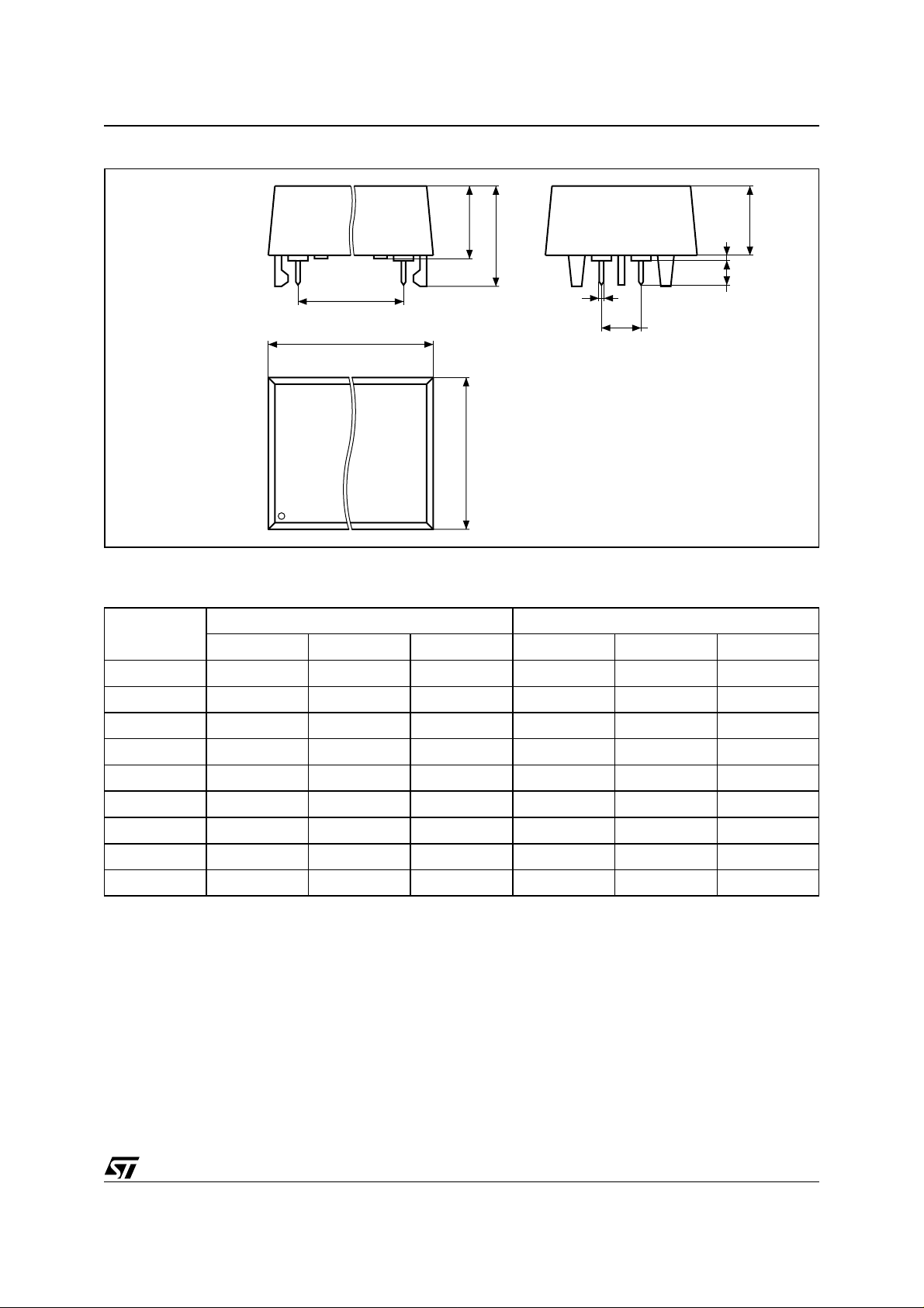
Figure 17. SH – 4-pin SNAPHAT Housing for 48mAh Battery & Crystal, Package Outline
eA
D
A1
A
B
eB
A3
L
E
SHTK
Note: D rawing is not to scale.
Table 14. SH – 4-pin SN APHAT Housing for 48mAh Battery & C r ystal, Package M ech. Dat a
Symb
Typ Min Max Typ Min Max
mm inches
A2
A 9.78 0.385
A1 6.73 7.24 0.265 0.285
A2 6.48 6.99 0.255 0.275
A3 0.38 0.015
B 0.46 0.56 0.018 0.022
D 21.21 21.84 0.835 0.860
E 14.22 14.99 0.560 0.590
eB 3.20 3.61 0.126 0.142
L 2.03 2.29 0.080 0.090
21/26
Page 22
M48T35, M48T35Y
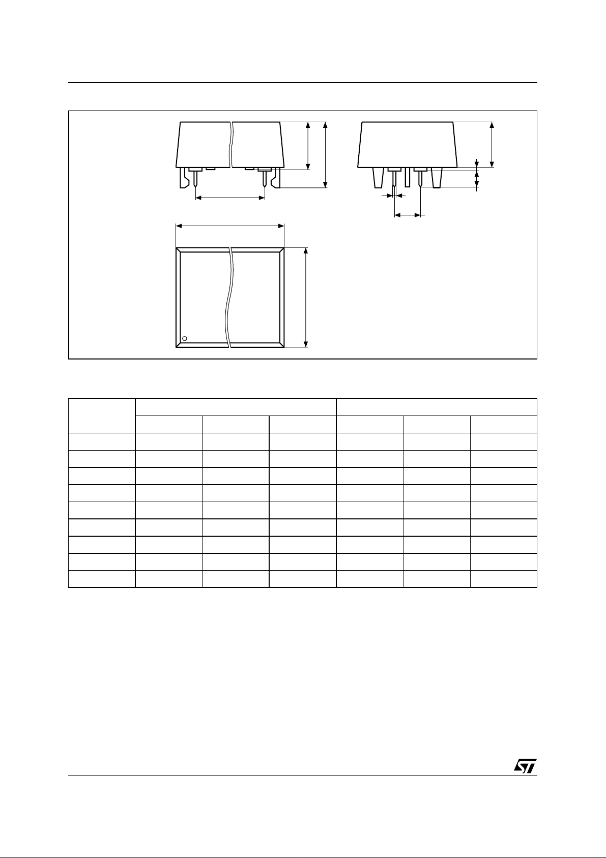
Figure 18. SH – 4-pin SNAPHAT Housing for 120mAh Battery & Crystal, Package Outline
eA
D
A1
A
B
eB
A3
L
E
SHTK
Note: D rawing is not to scale.
Table 15. SH – 4-pin SNAPHAT Housing for 120mAh Battery & Crystal, Package Mech. Data
Symb
Typ Min Max Typ Min Max
mm inches
A2
A 10.54 0.415
A1 8.00 8.51 0.315 0.335
A2 7.24 8.00 0.285 0.315
A3 0.38 0.015
B 0.46 0.56 0.018 0.022
D 21.21 21.84 0.835 0.860
E 17.27 18.03 0.680 0.710
eB 3.20 3.61 0.126 0.142
L 2.03 2.29 0.080 0.090
22/26
Page 23
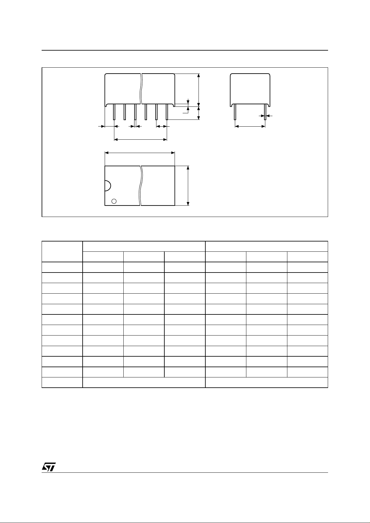
Figure 19. PMDIP28 – 28-pin Plastic DIP, Hybrid, Package Outline
M48T35, M48T35Y
A1AL
S
B
e1
eA
e3
D
N
E
1
Note: D rawing is not to scale.
Table 16. PMDIP28 – 28-pin Plastic DIP, Hybrid, Package Mechanical Data
Symb
Typ Min Max Typ Min Max
A 9.27 9.53 0.365 0.375
A1 0.38 0.015
B 0.43 0.58 0.017 0.023
mm inches
C
PMDIP
C 0.20 0.33 0.008 0.013
D 37.34 37.85 1.470 1.490
E 18.03 18.80 0.710 0.740
e1 2.29 2.79 0.090 0.110
e3 33.02 1.300
eA 14.99 16.00 0.590 0.630
L 3.05 3.81 0.120 0.150
S 1.91 2.67 0.075 0.105
N 28 28
23/26
Page 24
M48T35, M48T35Y
PART NUMBERING
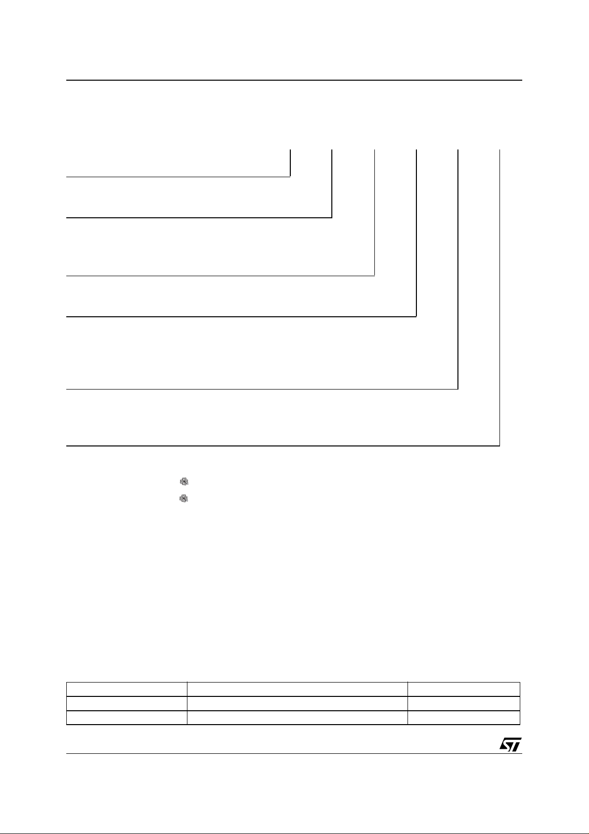
Table 17. Ordering Information Scheme
Example: M48T 35 –70 PC 1 E
Device Type
M48T
Supply Voltage and Write Protect Voltage
(1)
35
= VCC = 4.75 to 5.5V; V
35Y = V
= 4.5 to 5.5V; V
CC
Speed
–70 = 70ns
Package
PC = PCDIP28
(2)
MH
= SOH28
PM = PMDIP28 (NND)
(3)
= 4.5 to 4.75V
PFD
= 4.2 to 4.5V
PFD
Temperature Rang e
1 = 0 to 70°C
6 = –40 to 85°C
(4)
Shipping Method
For SOH28:
blank = Tubes (Not for New Design - Use E)
E = Lead-free Package (ECO PACK
F = Lead-free Package (ECO PACK
®
), Tubes
®
), Tape & Reel
TR = Tape & Reel (Not for New Design - Use F)
For PCDIP28:
blank = Tubes
Note: 1. The M48T35 part is offered with the PCDIP28 ( e.g., CAPHAT ) package only .
2. The SOIC package (SOH28) requires the SNAPHAT
BR12SH” in pl astic tube or “M4TXX-BR 12SHTR” in Tape & Reel form (see Table 18).
3. Thi s package is not to be used for N ew Design.
4. Avai lable in SOIC pa ckage only.
Caution: Do not place the SNAPHAT battery package “M4TXX-BR12SH” in conductive foam as it will drain the lithium button-cell battery.
®
battery package which is ordered separately under the part number “M4TXX-
For other options, or for more information on any aspect of this device, please contact the ST Sales Office
nearest you.
Table 18. SNAPHAT Battery Table
Part Number Description Package
M4T28-BR12SH Lithium Battery (48mAh) SNAPHAT SH
M4T32-BR12SH Lithium Battery (120mAh) SNAPHAT SH
24/26
Page 25
REVISION HISTORY
Table 19. Document Revision History
Date Rev. # Revision Details
November 1999 1.0 First Issue
t
07-Feb-00 1.1
04-Jun-01 2.0
31-Jul-01 2.1 Formatting changes based on latest document reviews
06-Mar-02 2.2
20-May-02 2.3 Modify reflow time and temperature footnotes (Table 6)
26-Jun-02 2.4 Add footnote to table (Table 11)
31-Mar-03 3.0 v2.2 template applied; data retention condition updated (Table 11)
10-Dec-03 4.0 Reformatted; update DC Characteristics (Table 9)
31-Mar-04 5.0 Reformatted; update Pb-free package information (Table 6, 17)
Description changed (Table 9)
DR
Reformatted; temp/voltage info. added to tables (Tables 8, 9, 3, 4, 10, 11); add Century
Bit text
Add PMDIP Packaging option, which is “Not for New Design” (NND) (Table 17, 16, and
Figure 19)
M48T35, M48T35Y
25/26
Page 26

M48T35, M48T35Y
Information furnished is believed to be accurate and reliable. However, STMicroelectronics a ssumes no responsibility fo r the c onsequences
of use of such information nor for any infringement of patents or other rights of third parties which may result from its use. No license is granted
by implication or otherwise under any patent or patent rights of STMicroelectronics. Specifications mentioned in this publication are subject
to change without notice. This publication supersedes and replaces all information previously supplied. STMicroelectronics products are not
authori zed for use as criti cal component s in life support devices or sys tems without express written approval of STMicroele ct ronics.
The ST logo is a registered trademark of STMi croelectronics.
All other na m es are the property of their respective ow ners.
© 2004 STMi croelectroni cs - All rights reserved
Australi a - B elgium - Braz i l - Canada - China - Czech Republ i c - Finland - France - Germany -
Hong Kong - India - Israel - It al y - Japan - Malays i a - Malta - Moroc co - Singapore -
STMicroelectroni cs GROUP OF COMPANIES
Spain - Sweden - Switzerland - United Kingdom - United States
www.st.com
26/26
 Loading...