

Page 1
M41T62, M41T63
M41T64, M41T65
Serial real-time clocks (RTCs) with alarm
Features
■ Serial real-time clock (RTC) with alarm
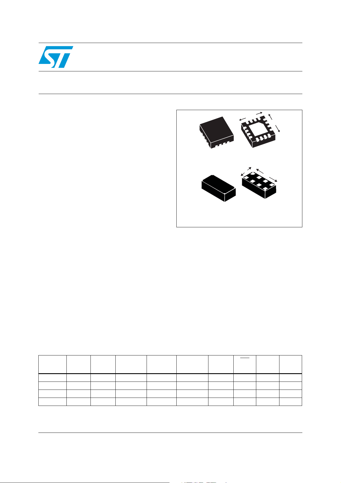
3mm
3mm
functions
– 400 kHz I
2
C serial interface
– Memory mapped registers for seconds,
minutes, hours, day, date, month, year, and
century
– Tenths/hundredths of seconds register
■ 350 nA timekeeping current at 3 V
■ Timekeeping down to 1.0 V
■ 1.3 V to 4.4 V I
– 4.4 V max V
2
C bus operating voltage
suitable for lithium-ion
CC
battery operation
■ Low operating current of 35 µA (at 400 kHz)
■ 32 KHz square wave output is on at power-up.
Suitable for driving a microcontroller in lowpower mode. Can be disabled.
(M41T62/63/64)
■ Programmable 1 Hz to 32 KHz square wave
output (M41T62/63/64)
■ Programmable alarm with interrupt function
(M41T62/65)
■ 32 KHz crystal oscillator integrates crystal load
capacitors, works with high series resistance
crystals
■ Oscillator stop detection monitors clock
operation
■ Accurate programmable watchdog
Embedded crystal LCC8
No external components required
■ Software clock calibration. Can adjust
timekeeping to withi
seconds per month)
■ Automatic leap year compensation
■ –40 to +85 °C operation
■ Two package options:
– Very small 3 mm x 3 mm, lead-free &
halogen-free (ECOPACK2
– Ultra-small 1.5 mm x 3.2 mm, lead-free &
halogen-free (ECOPACK2
leadless chip carrier with embedded
32 KHz crystal - no external oscillator
components required (M41T62)
QFN16
3 mm x 3 mm
1.5 mm
1.5 mm x 3.2 mm
n ±2 parts per million (±5
3.2 mm
®
) 16-lead QFN
®
) 8-pin ceramic
– 62.5 ms to 31 min timeout
Table 1. Device summary
Basic
RTC
M41T62 ✔✔ ✔ ✔ ✔ ✔✔
M41T63
1. Contact local ST sales office for availability.
(1)
✔✔ ✔ ✔ ✔ ✔ ✔
M41T64 ✔✔ ✔ ✔ ✔ ✔ ✔
M41T65 ✔✔ ✔ ✔ ✔ ✔✔
Alarms
OSC fail
detect
Watchdog
timer
Calibration
SQW
output
IRQ
output
WDO
output
F
32K
output
December 2011 Doc ID 10397 Rev 19 1/44
www.st.com
1
Page 2

Contents M41T62/63/64/65
Contents
1 Description . . . . . . . . . . . . . . . . . . . . . . . . . . . . . . . . . . . . . . . . . . . . . . . . . 6
2 Operation . . . . . . . . . . . . . . . . . . . . . . . . . . . . . . . . . . . . . . . . . . . . . . . . . 12
2.1 2-wire bus characteristics . . . . . . . . . . . . . . . . . . . . . . . . . . . . . . . . . . . . . 12
2.1.1 Bus not busy . . . . . . . . . . . . . . . . . . . . . . . . . . . . . . . . . . . . . . . . . . . . . 12
2.1.2 Start data transfer . . . . . . . . . . . . . . . . . . . . . . . . . . . . . . . . . . . . . . . . . 12
2.1.3 Stop data transfer . . . . . . . . . . . . . . . . . . . . . . . . . . . . . . . . . . . . . . . . . 12
2.1.4 Data valid . . . . . . . . . . . . . . . . . . . . . . . . . . . . . . . . . . . . . . . . . . . . . . . . 13
2.1.5 Acknowledge . . . . . . . . . . . . . . . . . . . . . . . . . . . . . . . . . . . . . . . . . . . . . 13
2.2 READ mode . . . . . . . . . . . . . . . . . . . . . . . . . . . . . . . . . . . . . . . . . . . . . . . 14
2.3 WRITE mode . . . . . . . . . . . . . . . . . . . . . . . . . . . . . . . . . . . . . . . . . . . . . . 16
3 Clock operation . . . . . . . . . . . . . . . . . . . . . . . . . . . . . . . . . . . . . . . . . . . . 17
3.1 RTC registers . . . . . . . . . . . . . . . . . . . . . . . . . . . . . . . . . . . . . . . . . . . . . . 18
3.2 Calibrating the clock . . . . . . . . . . . . . . . . . . . . . . . . . . . . . . . . . . . . . . . . . 24
3.3 Setting alarm clock registers . . . . . . . . . . . . . . . . . . . . . . . . . . . . . . . . . . 26
3.4 Watchdog timer . . . . . . . . . . . . . . . . . . . . . . . . . . . . . . . . . . . . . . . . . . . . 27
3.5 Watchdog output (WDO - M41T63/65 only) . . . . . . . . . . . . . . . . . . . . . . . 27
3.6 Square wave output (M41T62/63/64) . . . . . . . . . . . . . . . . . . . . . . . . . . . . 28
3.7 Full-time 32 KHz square wave output (M41T64) . . . . . . . . . . . . . . . . . . . 28
3.8 Century bits . . . . . . . . . . . . . . . . . . . . . . . . . . . . . . . . . . . . . . . . . . . . . . . 29
3.9 Output driver pin (M41T62/65) . . . . . . . . . . . . . . . . . . . . . . . . . . . . . . . . . 29
3.10 Oscillator stop detection . . . . . . . . . . . . . . . . . . . . . . . . . . . . . . . . . . . . . . 29
3.11 Initial power-on defaults . . . . . . . . . . . . . . . . . . . . . . . . . . . . . . . . . . . . . . 30
4 Maximum ratings . . . . . . . . . . . . . . . . . . . . . . . . . . . . . . . . . . . . . . . . . . . 31
5 DC and AC parameters . . . . . . . . . . . . . . . . . . . . . . . . . . . . . . . . . . . . . . 32
6 Package mechanical information . . . . . . . . . . . . . . . . . . . . . . . . . . . . . . 36
7 Part numbering . . . . . . . . . . . . . . . . . . . . . . . . . . . . . . . . . . . . . . . . . . . . 42
2/44 Doc ID 10397 Rev 19
Page 3

M41T62/63/64/65 Contents
8 Revision history . . . . . . . . . . . . . . . . . . . . . . . . . . . . . . . . . . . . . . . . . . . 43
Doc ID 10397 Rev 19 3/44
Page 4

List of tables M41T62/63/64/65
List of tables
Table 1. Device summary . . . . . . . . . . . . . . . . . . . . . . . . . . . . . . . . . . . . . . . . . . . . . . . . . . . . . . . . . . 1
Table 2. Signal names . . . . . . . . . . . . . . . . . . . . . . . . . . . . . . . . . . . . . . . . . . . . . . . . . . . . . . . . . . . . 9
Table 3. M41T62 register map . . . . . . . . . . . . . . . . . . . . . . . . . . . . . . . . . . . . . . . . . . . . . . . . . . . . . 20
Table 4. M41T63 register map . . . . . . . . . . . . . . . . . . . . . . . . . . . . . . . . . . . . . . . . . . . . . . . . . . . . . 21
Table 5. M41T64 register map . . . . . . . . . . . . . . . . . . . . . . . . . . . . . . . . . . . . . . . . . . . . . . . . . . . . . 22
Table 6. M41T65 register map . . . . . . . . . . . . . . . . . . . . . . . . . . . . . . . . . . . . . . . . . . . . . . . . . . . . . 23
Table 7. Alarm repeat modes . . . . . . . . . . . . . . . . . . . . . . . . . . . . . . . . . . . . . . . . . . . . . . . . . . . . . . 26
Table 8. Square wave output frequency . . . . . . . . . . . . . . . . . . . . . . . . . . . . . . . . . . . . . . . . . . . . . . 28
Table 9. Initial power-on default values . . . . . . . . . . . . . . . . . . . . . . . . . . . . . . . . . . . . . . . . . . . . . . 30
Table 10. Century bits examples . . . . . . . . . . . . . . . . . . . . . . . . . . . . . . . . . . . . . . . . . . . . . . . . . . . . 30
Table 11. Absolute maximum ratings . . . . . . . . . . . . . . . . . . . . . . . . . . . . . . . . . . . . . . . . . . . . . . . . . 31
Table 12. Operating and AC measurement conditions. . . . . . . . . . . . . . . . . . . . . . . . . . . . . . . . . . . . 32
Table 13. Capacitance . . . . . . . . . . . . . . . . . . . . . . . . . . . . . . . . . . . . . . . . . . . . . . . . . . . . . . . . . . . . 33
Table 14. DC characteristics. . . . . . . . . . . . . . . . . . . . . . . . . . . . . . . . . . . . . . . . . . . . . . . . . . . . . . . . 33
Table 15. Crystal electrical characteristics . . . . . . . . . . . . . . . . . . . . . . . . . . . . . . . . . . . . . . . . . . . . . 34
Table 16. Crystals suitable for use with M41T6x series RTCs . . . . . . . . . . . . . . . . . . . . . . . . . . . . . . 34
Table 17. Oscillator characteristics. . . . . . . . . . . . . . . . . . . . . . . . . . . . . . . . . . . . . . . . . . . . . . . . . . . 35
Table 18. AC characteristics . . . . . . . . . . . . . . . . . . . . . . . . . . . . . . . . . . . . . . . . . . . . . . . . . . . . . . . . 35
Table 19. QFN16 – 16-pin, quad, flat package, no-lead, 3 mm x 3 mm body size, mechanical data. 37
Table 20. LCC8 — 8-pin, 1.5 mm x 3.2 mm leadless chip carrier, mechanical data . . . . . . . . . . . . . 39
Table 21. Carrier tape dimensions for QFN16 3 mm x 3 mm package. . . . . . . . . . . . . . . . . . . . . . . . 40
Table 22. Reel dimensions for 12 mm carrier tape - QFN16 and LCC8 packages. . . . . . . . . . . . . . . 41
Table 23. Ordering information scheme . . . . . . . . . . . . . . . . . . . . . . . . . . . . . . . . . . . . . . . . . . . . . . . 42
Table 24. Document revision history . . . . . . . . . . . . . . . . . . . . . . . . . . . . . . . . . . . . . . . . . . . . . . . . . 43
4/44 Doc ID 10397 Rev 19
Page 5

M41T62/63/64/65 List of figures
List of figures
Figure 1. M41T62 logic diagram . . . . . . . . . . . . . . . . . . . . . . . . . . . . . . . . . . . . . . . . . . . . . . . . . . . . . 6
Figure 2. M41T63 logic diagram . . . . . . . . . . . . . . . . . . . . . . . . . . . . . . . . . . . . . . . . . . . . . . . . . . . . . 7
Figure 3. M41T64 logic diagram . . . . . . . . . . . . . . . . . . . . . . . . . . . . . . . . . . . . . . . . . . . . . . . . . . . . . 7
Figure 4. M41T65 logic diagram . . . . . . . . . . . . . . . . . . . . . . . . . . . . . . . . . . . . . . . . . . . . . . . . . . . . . 7
Figure 5. M41T62 connections . . . . . . . . . . . . . . . . . . . . . . . . . . . . . . . . . . . . . . . . . . . . . . . . . . . . . . 8
Figure 6. M41T63 connections . . . . . . . . . . . . . . . . . . . . . . . . . . . . . . . . . . . . . . . . . . . . . . . . . . . . . . 8
Figure 7. M41T64 connections . . . . . . . . . . . . . . . . . . . . . . . . . . . . . . . . . . . . . . . . . . . . . . . . . . . . . . 8
Figure 8. M41T65 connections . . . . . . . . . . . . . . . . . . . . . . . . . . . . . . . . . . . . . . . . . . . . . . . . . . . . . . 9
Figure 9. M41T62 block diagram . . . . . . . . . . . . . . . . . . . . . . . . . . . . . . . . . . . . . . . . . . . . . . . . . . . . . 9
Figure 10. M41T63 block diagram . . . . . . . . . . . . . . . . . . . . . . . . . . . . . . . . . . . . . . . . . . . . . . . . . . . . 10
Figure 11. M41T64 block diagram . . . . . . . . . . . . . . . . . . . . . . . . . . . . . . . . . . . . . . . . . . . . . . . . . . . . 10
Figure 12. M41T65 block diagram . . . . . . . . . . . . . . . . . . . . . . . . . . . . . . . . . . . . . . . . . . . . . . . . . . . . 10
Figure 13. Hardware hookup for SuperCap™ backup operation . . . . . . . . . . . . . . . . . . . . . . . . . . . . . 11
Figure 14. Serial bus data transfer sequence . . . . . . . . . . . . . . . . . . . . . . . . . . . . . . . . . . . . . . . . . . . 13
Figure 15. Acknowledgement sequence . . . . . . . . . . . . . . . . . . . . . . . . . . . . . . . . . . . . . . . . . . . . . . . 14
Figure 16. Slave address location . . . . . . . . . . . . . . . . . . . . . . . . . . . . . . . . . . . . . . . . . . . . . . . . . . . . 14
Figure 17. READ mode sequence . . . . . . . . . . . . . . . . . . . . . . . . . . . . . . . . . . . . . . . . . . . . . . . . . . . . 15
Figure 18. Alternative READ mode sequence . . . . . . . . . . . . . . . . . . . . . . . . . . . . . . . . . . . . . . . . . . . 15
Figure 19. WRITE mode sequence . . . . . . . . . . . . . . . . . . . . . . . . . . . . . . . . . . . . . . . . . . . . . . . . . . . 16
Figure 20. Buffer/transfer registers . . . . . . . . . . . . . . . . . . . . . . . . . . . . . . . . . . . . . . . . . . . . . . . . . . . 18
Figure 21. Crystal accuracy across temperature . . . . . . . . . . . . . . . . . . . . . . . . . . . . . . . . . . . . . . . . . 25
Figure 22. Calibration waveform . . . . . . . . . . . . . . . . . . . . . . . . . . . . . . . . . . . . . . . . . . . . . . . . . . . . . 25
Figure 23. Alarm interrupt reset waveform . . . . . . . . . . . . . . . . . . . . . . . . . . . . . . . . . . . . . . . . . . . . . . 26
Figure 24. AC measurement I/O waveform . . . . . . . . . . . . . . . . . . . . . . . . . . . . . . . . . . . . . . . . . . . . . 32
Figure 25. Crystal isolation example . . . . . . . . . . . . . . . . . . . . . . . . . . . . . . . . . . . . . . . . . . . . . . . . . . 32
Figure 26. Bus timing requirements sequence . . . . . . . . . . . . . . . . . . . . . . . . . . . . . . . . . . . . . . . . . . 35
Figure 27. QFN16 – 16-pin, quad, flat package, no-lead, 3 mm x 3 mm body size, outline . . . . . . . . 37
Figure 28. QFN16 – 16-pin, quad, flat package, no-lead, 3 x 3 mm, recommended footprint . . . . . . . 38
Figure 29. LCC8 — 8-pin, 1.5 mm x 3.2 mm leadless chip carrier, outline . . . . . . . . . . . . . . . . . . . . . 38
Figure 30. LCC8 — 8-pin, 1.5 mm x 3.2 mm leadless chip carrier, recommended footprint . . . . . . . . 39
Figure 31. Carrier tape for QFN16 3 mm x 3 mm package . . . . . . . . . . . . . . . . . . . . . . . . . . . . . . . . . 40
Figure 32. Carrier tape for LCC8 1.5 mm x 3.2 mm package . . . . . . . . . . . . . . . . . . . . . . . . . . . . . . . 40
Figure 33. Reel schematic . . . . . . . . . . . . . . . . . . . . . . . . . . . . . . . . . . . . . . . . . . . . . . . . . . . . . . . . . . 41
Doc ID 10397 Rev 19 5/44
Page 6

Description M41T62/63/64/65
1 Description
The M41T6x is a low-power serial real-time clock (RTC) with a built-in 32.768 kHz oscillator.
Eight registers are used for the clock/calendar function and are configured in binary coded
decimal (BCD) format. An additional 8 registers provide status/control of alarm, 32 KHz
output, calibration, and watchdog functions. Addresses and data are transferred serially via
a two line, bidirectional I
automatically after each WRITE or READ data byte.
Functions available to the user include a time-of-day clock/calendar, alarm interrupts
(M41T62/65), 32 KHz output (M41T62/63/64), programmable square wave output
(M41T62/63/64), and watchdog output (M41T63/65). The eight clock address locations
contain the century, year, month, date, day, hour, minute, second and tenths/hundredths of a
second in 24 hour BCD format. Corrections for 28-, 29- (leap year), 30- and 31-day months
are made automatically.
The M41T6x is supplied in two very small packages: a tiny, 3 mm x 3 mm 16-pin QFN which
requires a user-supplied 32 KHz crystal, and an ultra-small 1.5 mm x 3.2 mm LCC with
embedded crystal - no external crystal is required.
Figure 1. M41T62 logic diagram
2
C interface. The built-in address register is incremented
V
CC
1. Open drain.
2. Defaults to 32 KHz on power-up.
3. Not bonded on LCC package.
XI
XO
SCL
SDA
(3)
(3)
M41T62
V
SS
IRQ/OUT
(2)
SQW
(1)
AI09103
6/44 Doc ID 10397 Rev 19
Page 7

M41T62/63/64/65 Description
Figure 2. M41T63 logic diagram
V
CC
XI
XO
SCL
M41T63
WDO
SQW
(1)
(2)
SDA
V
SS
AI09189
1. Open drain.
2. Defaults to 32 KHz on power-up.
Figure 3. M41T64 logic diagram
V
CC
XI
XO
SCL
SDA
1. Open drain.
2. Defaults to 32 KHz on power-up.
Figure 4. M41T65 logic diagram
XI
XO
SCL
SDA
M41T64
V
SS
V
CC
M41T65
(1)
SQW
(2)
F
32K
(1)
WDO
IRQ/FT/OUT
AI09108
(1)
1. Open drain.
V
SS
AI09109
Doc ID 10397 Rev 19 7/44
Page 8

Description M41T62/63/64/65
Figure 5. M41T62 connections
CC
15
NC
14
V
NC
13
12
NC
SDA
1
8
SCL
NC
16
XI
1
SQW
V
XO
SS
2
QFN
3
(1)
4
6
5
SS
V
7
NC
NC
11
IRQ/OUT
SCL
10
9
SDA
8
NC
1. SQW output defaults to 32 KHz upon power-up.
2. Open drain.
Figure 6. M41T63 connections
NC
16
XI
1
XO
2
V
3
SS
(1)
SQW
4
5
V
SS
15
14
7
SQW
CC
V
NC
13
V
NC
8
(1)
SS
NC
NC
12
11
10
2
LCC
3
4
7
6
5
NC
IRQ/OUT
V
CC
(2)
AI09100
NC
(2)
WDO
SCL
9
SDA
AI09190
(2)
NC
6
NC
1. SQW output defaults to 32 KHz upon power-up.
2. Open drain.
Figure 7. M41T64 connections
NC
NC
15
14
6
NC
16
XI
1
XO
2
V
3
SS
(1)
32K
4
F
5
SS
V
1. Enabled on power-up.
2. Open drain.
8/44 Doc ID 10397 Rev 19
CC
NC
V
13
NC
12
(2)
SQW
11
SCL
10
9
SDA
8
7
NC
NC
AI09101
Page 9

M41T62/63/64/65 Description
Figure 8. M41T65 connections
15
CC
NC
V
14
6
7
NC
NC
WDO
NC
16
XI
1
XO
2
3
V
SS
(1)
4
5
SS
V
1. Open drain.
Table 2. Signal names
XI Oscillator input
XO Oscillator output
SDA Serial data input/output
SCL Serial clock input
IRQ/OUT Interrupt or OUT output (open drain)
/FT/OUT Interrupt, frequency test, or OUT output (open drain)
IRQ
SQW
F
32K
Programmable square wave - defaults to 32 KHz on power-up (open drain for
M41T64 only)
Dedicated 32 KHz output (M41T64 only)
WDO Watchdog timer output (open drain)
V
CC
V
SS
Supply voltage
Ground
13
NC
8
NC
NC
12
11
IRQ/FT/OUT
SCL
10
9
SDA
(1)
AI09102
Figure 9. M41T62 block diagram
(3)
XTAL
SDA
SCL
(3)
1. Open drain.
2. Defaults to 32 KHz on power-up.
3. Not bonded on embedded crystal (LCC) package.
32KHz
OSCILLATOR
I2C
INTERFACE
Doc ID 10397 Rev 19 9/44
REAL TIME CLOCK
CALENDAR
OSCILLATOR FAIL
DETECT
RTC W/ALARM
WATCHDOG
SQUARE WAVE
OFIE
AFE
SQWE
IRQ/OUT
(2)
SQW
AI08899a
(1)
Page 10

Description M41T62/63/64/65
Figure 10. M41T63 block diagram
REAL TIME CLOCK
CALENDAR
OSCILLATOR FAIL
XTAL
32KHz
OSCILLATOR
DETECT
RTC W/ALARM
SDA
I2C
INTERFACE
SCL
1. Open drain.
2. Defaults to 32 KHz on power-up.
Figure 11. M41T64 block diagram
XTAL
SDA
SCL
1. Defaults enabled on power-up.
2. Open drain.
32KHz
OSCILLATOR
I2C
INTERFACE
WATCHDOG
SQUARE WAVE
REAL TIME CLOCK
CALENDAR
OSCILLATOR FAIL
DETECT
RTC W/ALARM
WATCHDOG
SQUARE WAVE
SQWE
32KE
SQWE
WDO
SQW
F
32K
SQW
(1)
(2)
AI09191
(1)
(2)
AI09192
Figure 12. M41T65 block diagram
XTAL
SDA
SCL
1. Open drain.
10/44 Doc ID 10397 Rev 19
32KHz
OSCILLATOR
I2C
INTERFACE
REAL TIME CLOCK
CALENDAR
OSCILLATOR FAIL
DETECT
RTC W/ALARM
WATCHDOG
OFIE
FT
AFE
IRQ/FT/OUT
(1)
WDO
AI09193
(1)
Page 11

M41T62/63/64/65 Description
Figure 13. Hardware hookup for SuperCap™ backup operation
V
CC
(1)
MCU
V
CC
Por t
Reset Input
SQWIN
Serial Clock Line
Serial Data Line
32KHz CLKIN
AI10400b
V
XI
XO
V
CC
SS
M41T6x
IRQ/FT/OUT
WDO
SQW
F
(2)
(3)
(4)
SCL
SDA
32K
1. Diode required on open drain pin (M41T65 only) for SuperCap (or battery) backup. Low threshold BAT42
diode recommended.
2. For M41T62 and M41T65 (open drain).
3. For M41T63 and M41T65 (open drain).
4. For M41T64 (open drain).
Doc ID 10397 Rev 19 11/44
Page 12

Operation M41T62/63/64/65
2 Operation
The M41T6x clock operates as a slave device on the serial bus. Access is obtained by
implementing a start condition followed by the correct slave address (D0h). The 16 bytes
contained in the device can then be accessed sequentially in the following order:
st
● 1
● 2
● 3
● 4
● 5
● 6
● 7
● 8
● 9
● 10
● 11
● 16th byte: flags register
byte: tenths/hundredths of a second register
nd
byte: seconds register
rd
byte: minutes register
th
byte: hours register
th
byte: square wave/day register
th
byte: date register
th
byte: century/month register
th
byte: year register
th
byte: calibration register
th
byte: watchdog register
th
- 15th bytes: alarm registers
2.1 2-wire bus characteristics
The bus is intended for communication between different ICs. It consists of two lines: a bidirectional data signal (SDA) and a clock signal (SCL). Both the SDA and SCL lines must be
connected to a positive supply voltage via a pull-up resistor.
The following protocol has been defined:
● Data transfer may be initiated only when the bus is not busy.
● During data transfer, the data line must remain stable whenever the clock line is high.
● Changes in the data line, while the clock line is high, will be interpreted as control
signals.
Accordingly, the following bus conditions have been defined:
2.1.1 Bus not busy
Both data and clock lines remain high.
2.1.2 Start data transfer
A change in the state of the data line, from high to low, while the clock is high, defines the
START condition.
2.1.3 Stop data transfer
A change in the state of the data line, from low to high, while the clock is high, defines the
STOP condition.
12/44 Doc ID 10397 Rev 19
Page 13

M41T62/63/64/65 Operation
2.1.4 Data valid
The state of the data line represents valid data when after a start condition, the data line is
stable for the duration of the high period of the clock signal. The data on the line may be
changed during the Low period of the clock signal. There is one clock pulse per bit of data.
Each data transfer is initiated with a start condition and terminated with a stop condition.
The number of data bytes transferred between the start and stop conditions is not limited.
The information is transmitted byte-wide and each receiver acknowledges with a ninth bit.
By definition a device that gives out a message is called “transmitter,” the receiving device
that gets the message is called “receiver.” The device that controls the message is called
“master.” The devices that are controlled by the master are called “slaves.”
2.1.5 Acknowledge
Each byte of eight bits is followed by one acknowledge bit. This acknowledge bit is a low
level put on the bus by the receiver whereas the master generates an extra acknowledge
related clock pulse. A slave receiver which is addressed is obliged to generate an
acknowledge after the reception of each byte that has been clocked out of the slave
transmitter.
The device that acknowledges has to pull down the SDA line during the acknowledge clock
pulse in such a way that the SDA line is a stable Low during the high period of the
acknowledge related clock pulse. Of course, setup and hold times must be taken into
account. A master receiver must signal an end of data to the slave transmitter by not
generating an acknowledge on the last byte that has been clocked out of the slave. In this
case the transmitter must leave the data line high to enable the master to generate the
STOP condition.
Figure 14. Serial bus data transfer sequence
DATA LINE
STABLE
DATA VALID
CLOCK
DATA
STA RT
CONDITION
CHANGE OF
DATA ALLOWED
STOP
CONDITION
AI00587
Doc ID 10397 Rev 19 13/44
Page 14

Operation M41T62/63/64/65
Figure 15. Acknowledgement sequence
CLOCK PULSE FOR
ACKNOWLEDGEMENT
SCL FROM
MASTER
START
12 89
DATA OUTPUT
BY TRANSMITTER
DATA OUTPUT
BY RECEIVER
2.2 READ mode
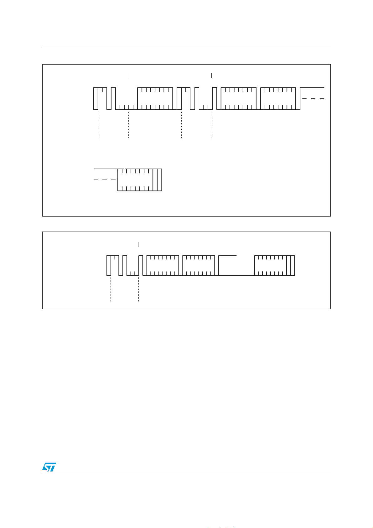
In this mode the master reads the M41T6x slave after setting the slave address (see
Figure 17 on page 15). Following the WRITE mode control bit (R/W
acknowledge bit, the word address 'An' is written to the on-chip address pointer. Next the
START condition and slave address are repeated followed by the READ mode control bit
(R/W
=1). At this point the master transmitter becomes the master receiver. The data byte
which was addressed will be transmitted and the master receiver will send an acknowledge
bit to the slave transmitter. the address pointer is only incremented on reception of an
acknowledge clock. The M41T6x slave transmitter will now place the data byte at address
An+1 on the bus, the master receiver reads and acknowledges the new byte and the
address pointer is incremented to “An+2.”
This cycle of reading consecutive addresses will continue until the master receiver sends a
STOP condition to the slave transmitter.
The system-to-user transfer of clock data will be halted whenever the address being read is
a clock address (00h to 07h). The update will resume due to a stop condition or when the
pointer increments to any non-clock address (08h-0Fh).
MSB LSB
AI00601
=0) and the
Note: This is true both in READ mode and WRITE mode.
An alternate READ mode may also be implemented whereby the master reads the M41T6x
slave without first writing to the (volatile) address pointer. The first address that is read is the
last one stored in the pointer (see Figure 18 on page 15).
Figure 16. Slave address location
STA RT A
14/44 Doc ID 10397 Rev 19
SLAVE ADDRESS
MSB
0100 011
R/W
LSB
AI00602
Page 15
M41T62/63/64/65 Operation
Figure 17. READ mode sequence
BUS ACTIVITY:
MASTER
SDA LINE
BUS ACTIVITY:
START
S
SLAVE
ADDRESS
R/W
ADDRESS (An)
ACK
DATA n+X
WORD
STOP
P
NO ACK
Figure 18. Alternative READ mode sequence
BUS ACTIVITY:
MASTER
STA RT
R/W
START
S
ACK
ADDRESS
SLAVE
R/W
DATA n DATA n+1
ACK
ACK
ACK
AI00899
STOP
BUS ACTIVITY:
S
SLAVE
ADDRESS
DATA n DATA n+1 DATA n+X
ACK
ACK
ACK
ACK
PSDA LI NE
NO ACK
AI00895
Doc ID 10397 Rev 19 15/44
Page 16
Operation M41T62/63/64/65
2.3 WRITE mode
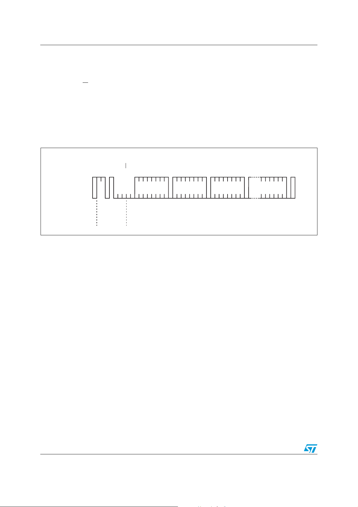
In this mode the master transmitter transmits to the M41T6x slave receiver. Bus protocol is
shown in Figure 19 on page 16. Following the START condition and slave address, a logic '0'
(R/W
=0) is placed on the bus and indicates to the addressed device that word address “An”
will follow and is to be written to the on-chip address pointer. The data word to be written to
the memory is strobed in next and the internal address pointer is incremented to the next
address location on the reception of an acknowledge clock. The M41T6x slave receiver will
send an acknowledge clock to the master transmitter after it has received the slave address
see Figure 16 on page 14 and again after it has received the word address and each data
byte.
Figure 19. WRITE mode sequence
BUS ACTIVITY:
MASTER
BUS ACTIVITY:
START
S
ADDRESS
SLAVE
R/W
WORD
ADDRESS (An)
ACK
DATA n DATA n+1 DATA n+X
ACK
ACK
ACK
STOP
PSDA LINE
ACK
AI00591
16/44 Doc ID 10397 Rev 19
Page 17

M41T62/63/64/65 Clock operation
3 Clock operation
The M41T6x is driven by a quartz-controlled oscillator with a nominal frequency of
32.768 kHz. The accuracy of the real-time clock depends on the frequency of the quartz
crystal that is used as the time-base for the RTC.
The eight byte clock register (see Table 3: M41T62 register map, Table 4: M41T63 register
map, Table 5: M41T64 register map, and Table 6: M41T65 register map) is used to both set
the clock and to read the date and time from the clock, in a binary coded decimal format.
Tenths/hundredths of seconds, seconds, minutes, and hours are contained within the first
four registers.
A WRITE to any clock register will result in the tenths/hundredths of seconds being reset to
“00,” and tenths/hundredths of seconds cannot be written to any value other than “00.”
Bits D0 through D2 of register 04h contain the day (day of week). Registers 05h, 06h, and
07h contain the date (day of month), month, and years. The ninth clock register is the
calibration register (this is described in the clock calibration section). Bit D7 of register 01h
contains the STOP bit (ST). Setting this bit to a '1' will cause the oscillator to stop. When
reset to a '0' the oscillator restarts within one second (typical).
Upon initial power-up, the user should set the ST bit to a '1,' then immediately reset the ST
bit to '0.' This provides an additional “kick-start” to the oscillator circuit.
Bit D7 of register 02h (minute register) contains the oscillator fail interrupt enable bit (OFIE).
When the user sets this bit to '1,' any condition which sets the oscillator fail bit (OF) (see
Oscillator stop detection on page 29) will also generate an interrupt output.
Bits D6 and D7 of clock register 06h (century/month register) contain the CENTURY bit 0
(CB0) and CENTURY bit 1 (CB1).
A WRITE to ANY location within the first eight bytes of the clock register (00h-07h),
including the OFIE bit, RS0-RS3 bit, and CB0-CB1 bits will result in an update of the system
clock and a reset of the divider chain. This could result in an inadvertent change of the
current time. These non-clock related bits should be written prior to setting the clock, and
remain unchanged until such time as a new clock time is also written.
The eight clock registers may be read one byte at a time, or in a sequential block. Provision
has been made to assure that a clock update does not occur while any of the eight clock
addresses are being read. If a clock address is being read, an update of the clock registers
will be halted. This will prevent a transition of data during the READ.
Doc ID 10397 Rev 19 17/44
Page 18
Clock operation M41T62/63/64/65
3.1 RTC registers
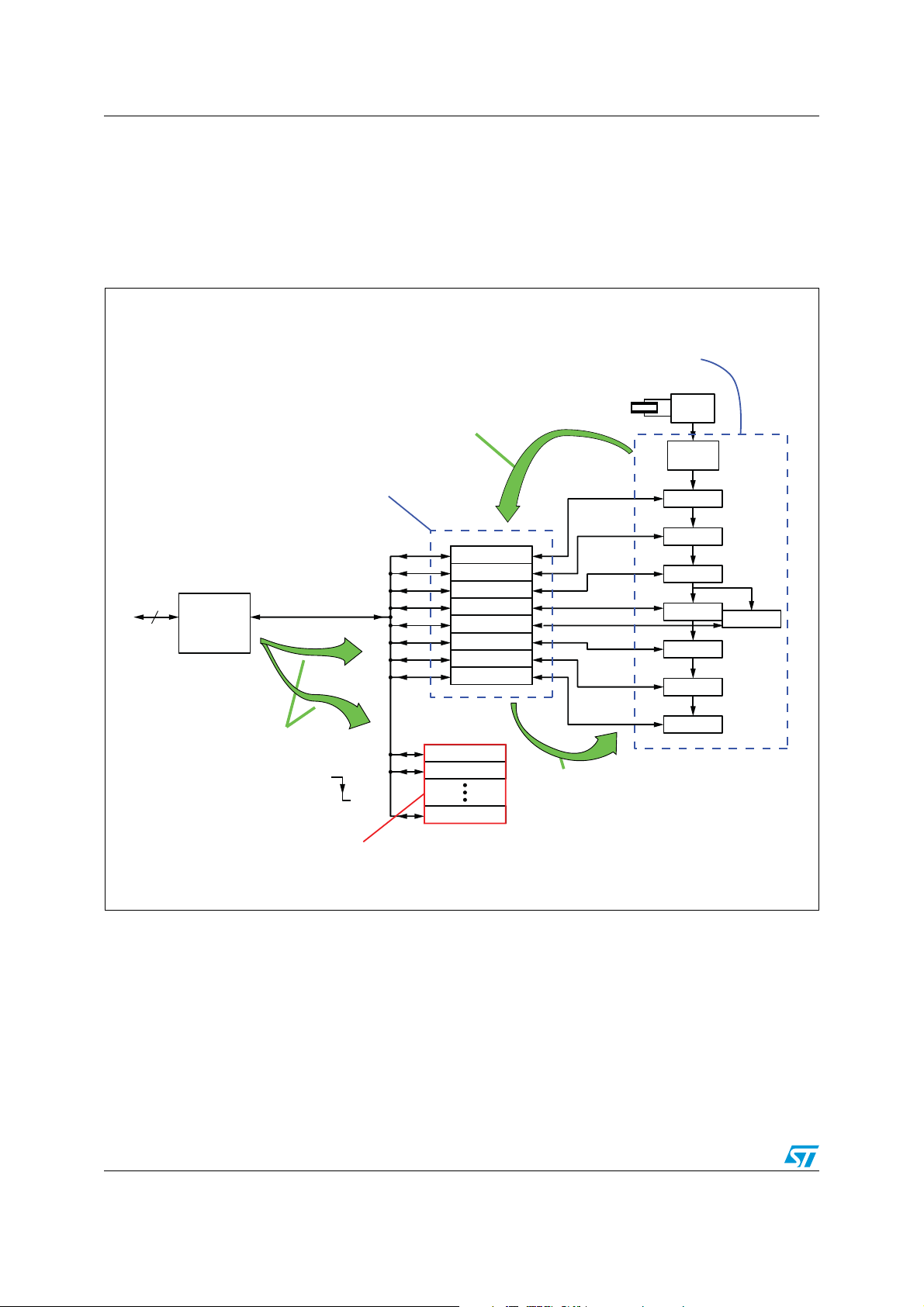
The M41T6x user interface is comprised of 16 memory mapped registers which include
clock, calibration, alarm, watchdog, flags, and square wave control. The eight clock
counters are accessed indirectly via a set of buffer/transfer registers while the other eight
registers are directly accessed. Data in the clock and alarm registers is in BCD format.
Figure 20. Buffer/transfer registers
CLOCK COUNTERS ARE
ACCESSED INDIRECTLY
THRU BUFFER/TRANSFER
REGISTERS
I2C
2
I2C
INTERFACE
AT START OF READ, UDATES FROM COUNTERS
ARE HALTED AND PRESENT TIME IS FROZEN
IN BUFFER/TRANSFER REGISTERS.
READ / WRITE
BUFFER
TRANSFER
REGISTERS
SECONDS
MINUTES
HOURS
DAY-OF-WEEK
DATE
MONTHS
YEARS
CENTURIES
32KHz
OSC
DIVIDE BY
32768
1 Hz
COUNTER
COUNTER
COUNTER
COUNTER
COUNTER
COUNTER
COUNTER
NON-CLOCK
DATA TRANSFERRED
OUT OF I
ON 8
OF SCL (ON WRITES)
2
C INTERFACE
th
FALLING EDGE
NON-CLOCK REGISTERS
ARE DIRECTLY ACCESSED
REGISTERS
CALIBRATION
WATCHDOG
FLAGS
Updates
During normal operation when the user is not accessing the device, the buffer/transfer
registers are kept updated with a copy of the RTC counters. At the start of an I
write cycle, the updating is halted and the present time is frozen in the buffer/transfer
registers.
Reads of the clock registers
By halting the updates at the start of an I2C access, the user is ensured that all the data
transferred out during a read sequence comes from the same instant in time.
18/44 Doc ID 10397 Rev 19
COUNTER
ON WRITES, DATA TRANSFERRED
FROM BUFFERS TO COUNTERS
WHEN ADDRESS POINTER
INCREMENTS TO 8 OR WHEN I
STOP CONDITION IS RECEIVED
2
C
2
C read or
AM04890v1
Page 19

M41T62/63/64/65 Clock operation
Write timing
When writing to the device, the data is shifted into the M41T62's I2C interface on the rising
edge of the SCL signal. As shown in Figure 20, on the 8th clock cycle, the data is
transferred from the I
2
C block into whichever register is being pointed to by the address
pointer (not shown).
Writes to the clock registers (addresses 0-7)
Data written to the clock registers (addresses 0-7) is held in the buffer registers until the
address pointer increments to 8, or an I
2
C stop condition occurs, at which time the data in
the buffer/registers is simultaneously copied into the counters, and then the clock is restarted.
Doc ID 10397 Rev 19 19/44
Page 20
Clock operation M41T62/63/64/65
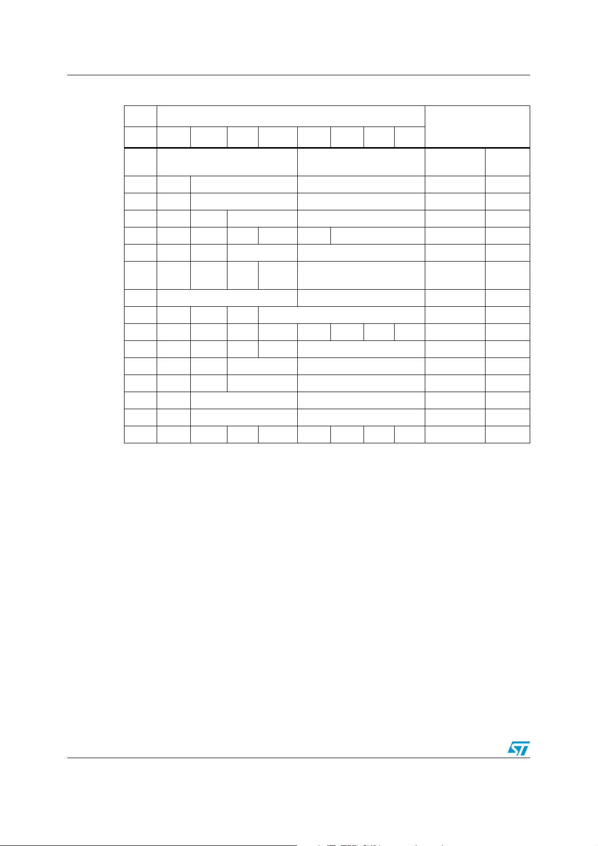
Table 3. M41T62 register map
Addr
D7 D6 D5 D4 D3 D2 D1 D0
00h 0.1 seconds 0.01 seconds
Function/range BCD
format
10ths/100ths
of seconds
00-99
01h ST 10 seconds Seconds Seconds 00-59
02h OFIE 10 minutes Minutes Minutes 00-59
03h 0 0 10 hours Hours (24-hour format) Hours 00-23
04h RS3 RS2 RS1 RS0 0 Day of week Day 01-7
05h 0 0 10 date Date: day of month Date 01-31
06h CB1 CB0 0 10M Month
Century/
month
0-3/01-12
07h 10 years Year Year 00-99
08h OUT 0 S Calibration Calibration
09h RB2 BMB4 BMB3 BMB2 BMB1 BMB0 RB1 RB0 Watchdog
0Ah AFE SQWE 0 Al 10M Alarm month Al month 01-12
0Bh RPT4 RPT5 AI 10 date Alarm date Al date 01-31
0Ch RPT3 0 AI 10 hour Alarm hour Al hour 00-23
0Dh RPT2 Alarm 10 minutes Alarm minutes Al min 00-59
0Eh RPT1 Alarm 10 seconds Alarm seconds Al sec 00-59
0Fh WDF AF 0 0 0 OF 0 0 Flags
Keys:
0 = must be set to '0'
AF = alarm flag (read only)
AFE = alarm flag enable flag
BMB0 - BMB4 = watchdog multiplier bits
CB0-CB1 = century bits
OF = oscillator fail bit
OFIE = oscillator fail interrupt enable bit
OUT = output level
RB0 - RB2 = watchdog resolution bits
RPT1-RPT5 = alarm repeat mode bits
RS0-RS3 = SQW frequency bits
S = sign bit
SQWE = square wave enable bit
ST = stop bit
WDF = watchdog flag bit (read only)
20/44 Doc ID 10397 Rev 19
Page 21
M41T62/63/64/65 Clock operation
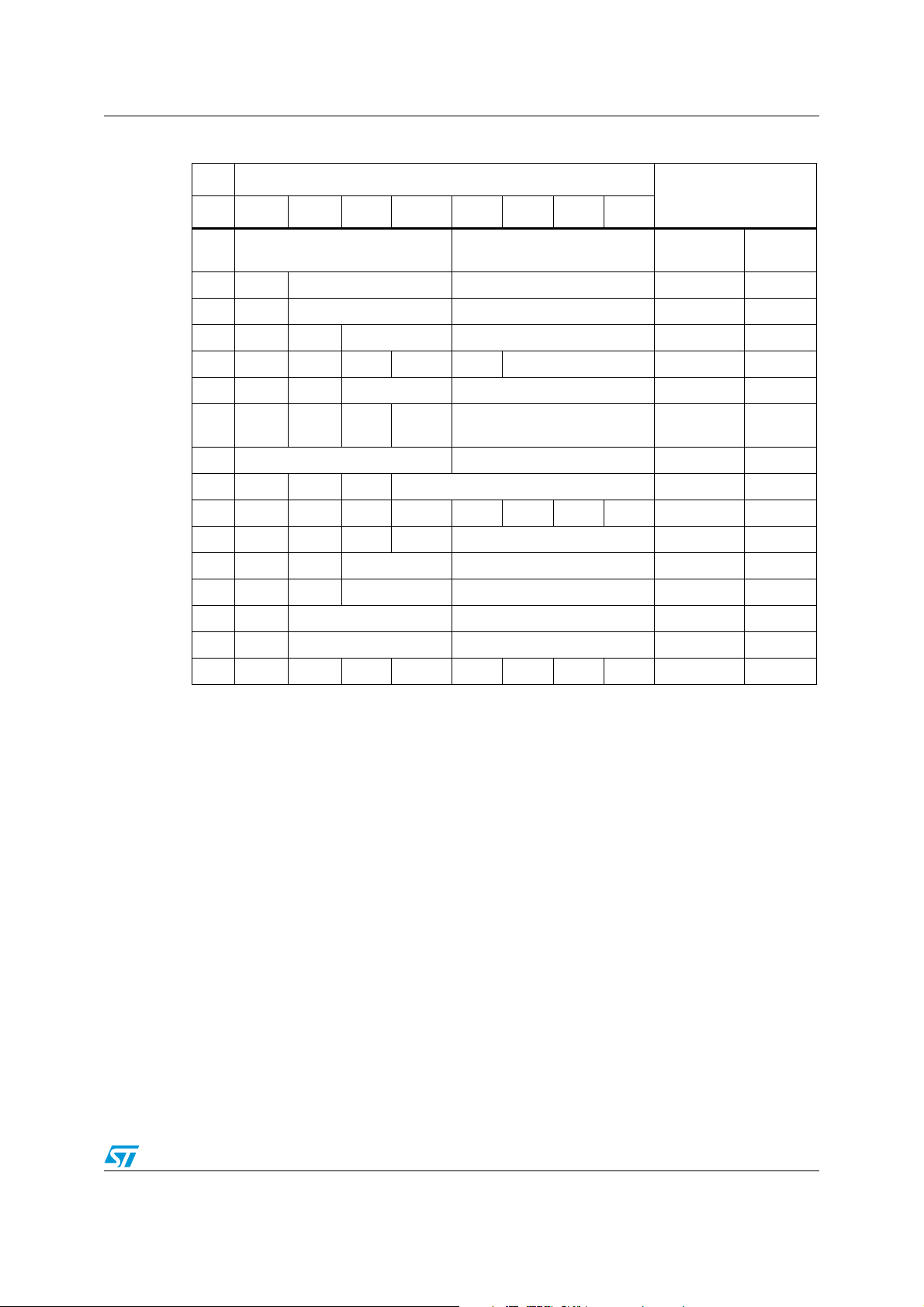
Table 4. M41T63 register map
Addr
D7 D6 D5 D4 D3 D2 D1 D0
00h 0.1 seconds 0.01 seconds
Function/range BCD
format
10ths/100ths
of seconds
00-99
01h ST 10 seconds Seconds Seconds 00-59
02h 0 10 minutes Minutes Minutes 00-59
03h 0 0 10 hours Hours (24-hour format) Hours 00-23
04h RS3 RS2 RS1 RS0 0 Day of week Day 01-7
05h 0 0 10 date Date: day of month Date 01-31
06h CB1 CB0 0 10M Month
Century/
month
0-3/01-12
07h 10 years Year Year 00-99
08h 0 0 S Calibration Calibration
09h RB2 BMB4 BMB3 BMB2 BMB1 BMB0 RB1 RB0 Watchdog
0Ah 0 SQWE 0 Al 10M Alarm month Al Month 01-12
0Bh RPT4 RPT5 AI 10 date Alarm date Al date 01-31
0Ch RPT3 0 AI 10 hour Alarm hour Al hour 00-23
0Dh RPT2 Alarm 10 minutes Alarm minutes Al min 00-59
0Eh RPT1 Alarm 10 seconds Alarm seconds Al sec 00-59
0Fh WDF AF 0 0 0 OF 0 0 Flags
Keys:
0 = must be set to '0'
AF = alarm flag (read only)
BMB0 - BMB4 = watchdog multiplier bits
CB0-CB1 = century bits
OF = oscillator fail bit
RB0 - RB2 = watchdog resolution bits
RPT1-RPT5 = alarm repeat mode bits
RS0-RS3 = SQW frequency bits
S = sign bit
SQWE = square wave enable bit
ST = stop bit
WDF = watchdog flag bit (read only)
Doc ID 10397 Rev 19 21/44
Page 22
Clock operation M41T62/63/64/65
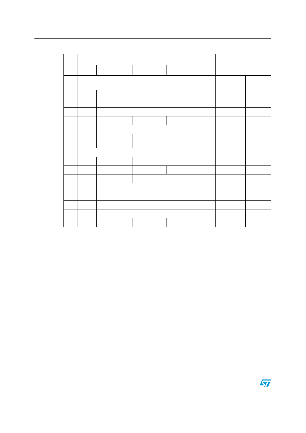
Table 5. M41T64 register map
Addr
D7 D6 D5 D4 D3 D2 D1 D0
00h 0.1 seconds 0.01 seconds
Function/range BCD
format
10ths/100ths
of seconds
00-99
01h ST 10 seconds Seconds Seconds 00-59
02h 0 10 minutes Minutes Minutes 00-59
03h 0 0 10 hours Hours (24-hour format) Hours 00-23
04h RS3 RS2 RS1 RS0 0 Day of week Day 01-7
05h 0 0 10 Date Date: day of month Date 01-31
06h CB1 CB0 0 10M Month
Century/
month
0-3/01-12
07h 10 years Year Year 00-99
08h 0 0 S Calibration Calibration
09h RB2 BMB4 BMB3 BMB2 BMB1 BMB0 RB1 RB0 Watchdog
0Ah 0 SQWE 32KE Al 10M Alarm month Al month 01-12
0Bh RPT4 RPT5 AI 10 date Alarm date Al date 01-31
0Ch RPT3 0 AI 10 hour Alarm hour Al hour 00-23
0Dh RPT2 Alarm 10 minutes Alarm minutes Al min 00-59
0Eh RPT1 Alarm 10 seconds Alarm seconds Al sec 00-59
0Fh WDF AF 0 0 0 OF 0 0 Flags
Keys:
0 = must be set to '0'
32KE = 32 KHz enable bit
AF = alarm flag (read only)
BMB0 - BMB4 = watchdog multiplier bits
CB0-CB1 = century bits
OF = oscillator fail bit
RB0 - RB2 = watchdog resolution bits
RPT1-RPT5 = alarm repeat mode bits
RS0-RS3 = SQW frequency bits
S = sign bit
SQWE = square wave enable bit
ST = stop bit
WDF = watchdog flag bit (read only)
22/44 Doc ID 10397 Rev 19
Page 23
M41T62/63/64/65 Clock operation
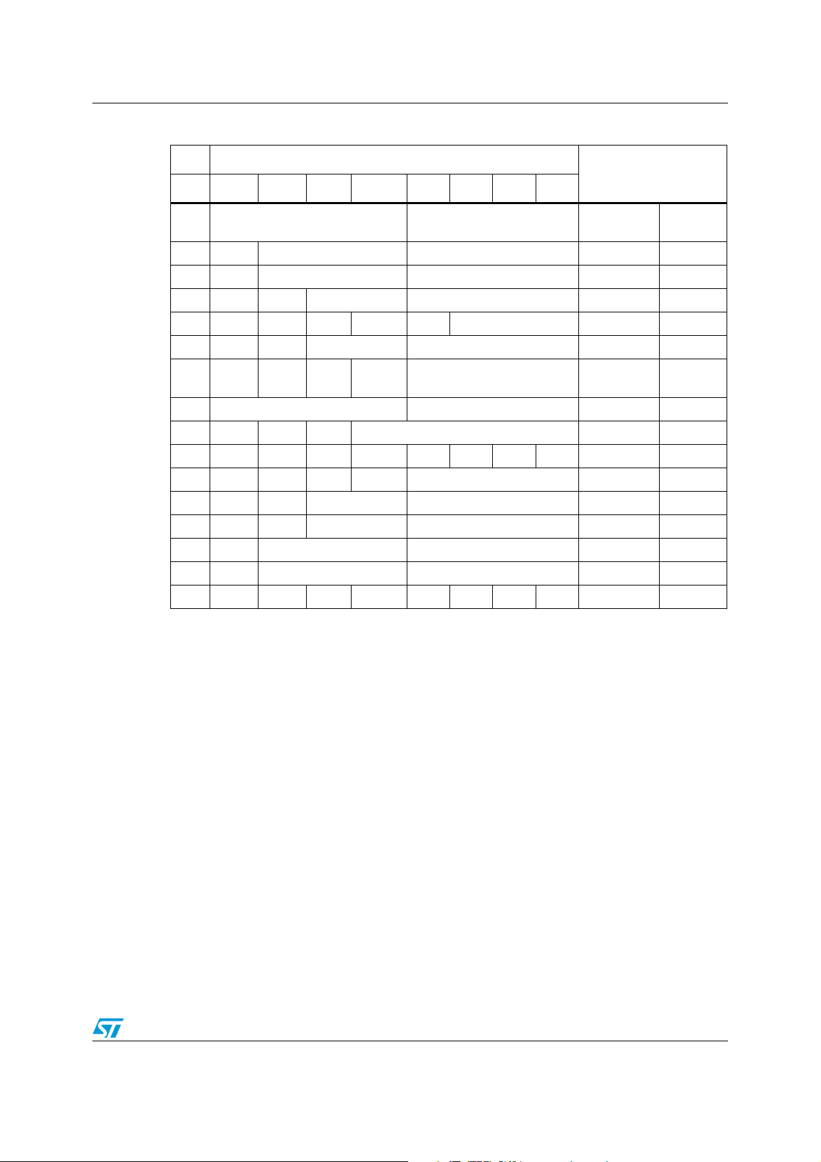
Table 6. M41T65 register map
Addr
D7 D6 D5 D4 D3 D2 D1 D0
00h 0.1 seconds 0.01 seconds
Function/range BCD
format
10ths/100ths
of seconds
00-99
01h ST 10 seconds Seconds Seconds 00-59
02h OFIE 10 minutes Minutes Minutes 00-59
03h 0 0 10 hours Hours (24-hour format) Hours 00-23
04h 0 0 0 0 0 Day of week Day 01-7
05h 0 0 10 date Date: day of month Date 01-31
06h CB1 CB0 0 10M Month
Century/
month
0-3/01-12
07h 10 years Year Year 00-99
08h OUT FT S Calibration Calibration
09h RB2 BMB4 BMB3 BMB2 BMB1 BMB0 RB1 RB0 Watchdog
0Ah AFE 0 0 Al 10M Alarm month Al month 01-12
0Bh RPT4 RPT5 AI 10 date Alarm date Al date 01-31
0Ch RPT3 0 AI 10 hour Alarm hour Al hour 00-23
0Dh RPT2 Alarm 10 minutes Alarm minutes Al min 00-59
0Eh RPT1 Alarm 10 seconds Alarm seconds Al sec 00-59
0Fh WDF AF 0 0 0 OF 0 0 Flags
Keys:
0 = must be set to '0'
AF = alarm flag (read only)
AFE = alarm flag enable flag
BMB0 - BMB4 = watchdog multiplier bits
CB0-CB1 = century bits
FT = frequency test bit
OF = oscillator fail bit
OFIE = oscillator fail interrupt enable bit
OUT = output level
RB0 - RB2 = watchdog resolution bits
RPT1-RPT5 = alarm repeat mode bits
S = sign bit
ST = stop bit
WDF = watchdog flag bit (read only)
Doc ID 10397 Rev 19 23/44
Page 24

Clock operation M41T62/63/64/65
3.2 Calibrating the clock
The M41T6x real-time clock is driven by a quartz controlled oscillator with a nominal
frequency of 32,768 Hz. This provides the time-base for the RTC. The accuracy of the clock
depends on the frequency accuracy of the crystal, and the match between the capacitive
load of the oscillator circuit and the capacitive load for which the crystal was trimmed. The
M41T6x oscillator is designed for use with a 6 - 7 pF crystal load capacitance. When the
calibration circuit is properly employed, accuracy improves to better than ±2 ppm at 25 °C.
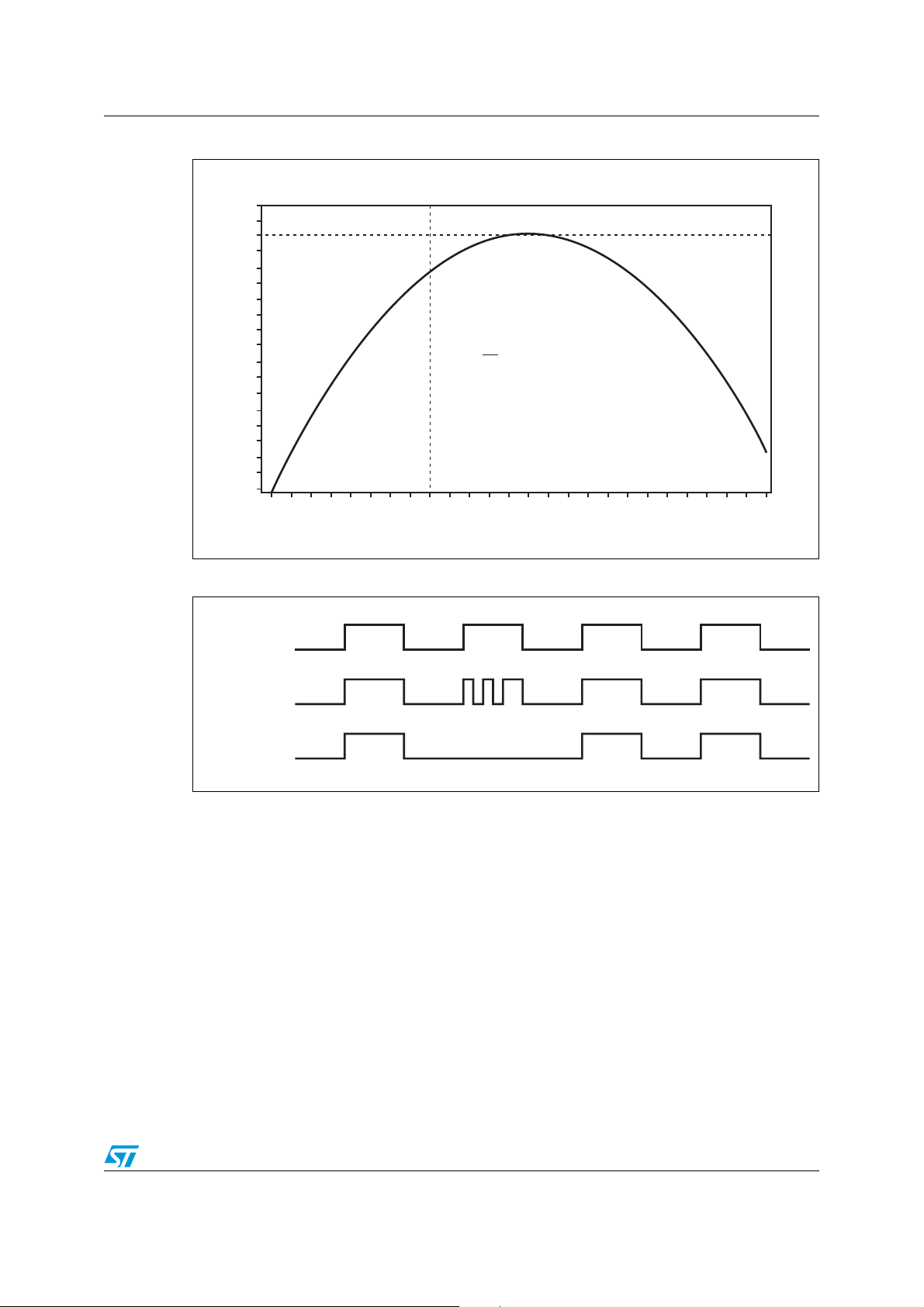
The oscillation rate of crystals changes with temperature (see Figure 21 on page 25).
Therefore, the M41T6x design employs periodic counter correction. The calibration circuit
adds or subtracts counts from the oscillator divider circuit at the divide by 256 stage, as
shown in Figure 22 on page 25. The number of times pulses which are blanked (subtracted,
negative calibration) or split (added, positive calibration) depends upon the value loaded into
the five calibration bits found in the calibration register. Adding counts speeds the clock up,
subtracting counts slows the clock down.
The calibration bits occupy the five lower order bits (D4-D0) in the calibration register (08h).
These bits can be set to represent any value between 0 and 31 in binary form. Bit D5 is a
sign bit; '1' indicates positive calibration, '0' indicates negative calibration. Calibration occurs
within a 64 minute cycle. The first 62 minutes in the cycle may, once per minute, have one
second either shortened by 128 or lengthened by 256 oscillator cycles. If a binary '1' is
loaded into the register, only the first 2 minutes in the 64 minute cycle will be modified; if a
binary 6 is loaded, the first 12 will be affected, and so on.
Therefore, each calibration step has the effect of adding 512 or subtracting 256 oscillator
cycles for every 125,829,120 actual oscillator cycles, that is +4.068 or –2.034 ppm of
adjustment per calibration step in the calibration register.
Assuming that the oscillator is running at exactly 32,768 Hz, each of the 31 increments in
the calibration byte would represent +10.7 or –5.35 seconds per day which corresponds to a
total range of +5.5 or –2.75 minutes per month (see Figure 22 on page 25).
Two methods are available for ascertaining how much calibration a given M41T6x may
require:
● The first involves setting the clock, letting it run for a month and comparing it to a known
accurate reference and recording deviation over a fixed period of time. Calibration
values, including the number of seconds lost or gained in a given period, can be found
in application note AN934, “How to use the digital calibration feature in TIMEKEEPER
®
and serial real-time clock (RTC) products.” This allows the designer to give the end user
the ability to calibrate the clock as the environment requires, even if the final product is
packaged in a non-user serviceable enclosure. The designer could provide a simple
utility that accesses the calibration byte.
● The second approach is better suited to a manufacturing environment, and involves the
use of either the SQW pin (M41T62/63/64) or the IRQ
/FT/OUT pin (M41T65). The
SQW pin will toggle at 512 Hz when RS3 = '0,' RS2 = '1,' RS1 = '1,' RS0 = '0,' SQ
WE = '1,' and ST = '0.' Alternatively, for the M41T65, the IRQ
/FT/OUT pin will toggle at
512 Hz when FT and OUT bits = '1' and ST = '0.'
Any deviation from 512 Hz indicates the degree and direction of oscillator frequency shift at
the test temperature. For example, a reading of 512.010124 Hz would indicate a +20 ppm
oscillator frequency error, requiring a –10 (XX001010) to be loaded into the calibration byte
for correction. Note that setting or changing the calibration byte does not affect the
frequency test or square wave output frequency.
24/44 Doc ID 10397 Rev 19
Page 25
M41T62/63/64/65 Clock operation
Figure 21. Crystal accuracy across temperature
Frequency (ppm)
20
0
–20
–40
–60
2
)
O
= 25°C ± 5°C
T
O
2
80–10–20–30–40
AI07888
–80
–100
–120
–140
–160
ΔF
= K x (T – T
F
= –0.036 ppm/°C2 ± 0.006 ppm/°C
K
0 10203040506070
Temperature °C
Figure 22. Calibration waveform
NORMAL
POSITIVE
CALIBRATION
NEGATIVE
CALIBRATION
AI00594b
Doc ID 10397 Rev 19 25/44
Page 26
Clock operation M41T62/63/64/65
3.3 Setting alarm clock registers
Address locations 0Ah-0Eh contain the alarm settings. The alarm can be configured to go
off at a prescribed time on a specific month, date, hour, minute, or second, or repeat every
year, month, day, hour, minute, or second. Bits RPT5–RPT1 put the alarm in the repeat
mode of operation. Table 7 on page 26 shows the possible configurations. Codes not listed
in the table default to the once per second mode to quickly alert the user of an incorrect
alarm setting.
When the clock information matches the alarm clock settings based on the match criteria
defined by RPT5–RPT1, the AF (alarm flag) is set. If AFE (alarm flag enable) is also set
(M41T62/65), the alarm condition activates the IRQ
alarm, write '0' to the alarm date register and to RPT5–RPT1.
Note: If the address pointer is allowed to increment to the flag register address, an alarm condition
will not cause the interrupt/flag to occur until the address pointer is moved to a different
address. It should also be noted that if the last address written is the “Alarm Seconds,” the
address pointer will increment to the flag address, causing this situation to occur.
/OUT or IRQ/FT/OUT pin. To disable the
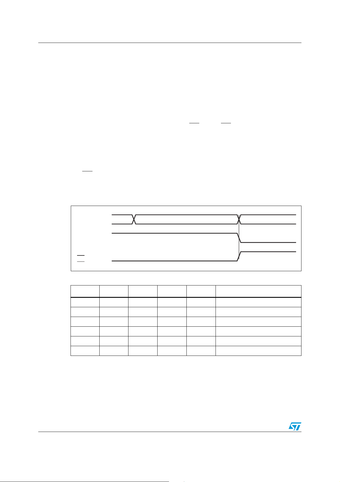
The IRQ
output is cleared by a READ to the flags register as shown in Figure 23 on
page 26. A subsequent READ of the flags register is necessary to see that the value of the
alarm flag has been reset to '0.'
Figure 23. Alarm interrupt reset waveform
Register address
ALARM FLAG BIT (AF)
IRQ/OUT or
IRQ/FT/OUT
Table 7. Alarm repeat modes
RPT5 RPT4 RPT3 RPT2 RPT1 Alarm setting
1 1 1 1 1 Once per second
1 1 1 1 0 Once per minute
1 1 1 0 0 Once per hour
1 1 0 0 0 Once per day
1 0 0 0 0 Once per month
0 0 0 0 0 Once per year
0Fh0Eh 00h
HIGH-Z
AI08898
26/44 Doc ID 10397 Rev 19
Page 27

M41T62/63/64/65 Clock operation
3.4 Watchdog timer
The watchdog timer can be used to detect an out-of-control microprocessor. The user
programs the watchdog timer by setting the desired amount of time-out into the watchdog
register, address 09h.
Bits BMB4-BMB0 store a binary multiplier and the three bits RB2-RB0 select the resolution
where:
000=1/16 second (16 Hz);
001=1/4 second (4 Hz);
010=1 second (1 Hz);
011=4 seconds (1/4 Hz); and
100 = 1 minute (1/60 Hz).
Note: Invalid combinations (101, 110, and 111) will NOT enable a watchdog time-out. Setting
BMB4-BMB0 = 00000 with any combination of RB2-RB0, other than 000, will result in an
immediate watchdog time-out.
The amount of time-out is then determined to be the multiplication of the five-bit multiplier
value with the resolution. (For example: writing 00001110 in the watchdog register = 3*1 or 3
seconds). If the processor does not reset the timer within the specified period, the M41T6x
sets the WDF (watchdog flag) and generates an interrupt on the IRQ
watchdog output pulse (M41T63 and M41T65 only) on the WDO
can only be reset by having the microprocessor perform a WRITE of the watchdog register.
The time-out period then starts over.
pin (M41T62), or a
pin. The watchdog timer
Should the watchdog timer time-out, any value may be written to the watchdog register in
order to clear the IRQ
programmed to a new value. A READ of the flags register will reset the watchdog flag (bit
D7; register 0Fh). The watchdog function is automatically disabled upon power-up, and the
watchdog register is cleared.
Note: A WRITE to any clock register will restart the watchdog timer.
pin. A value of 00h will disable the watchdog function until it is again
3.5 Watchdog output (WDO - M41T63/65 only)
If the processor does not reset the watchdog timer within the specified period, the watchdog
output (WDO
connected to the reset input of the processor in order to generate a processor reset. After a
watchdog time-out occurs, the timer will remain disabled until such time as a new
countdown value is written into the watchdog register.
Note: The crystal oscillator must be running for the WDO
The WDO
on page 33).
) will pulse low for t
output is an N-channel, open drain output driver (with IOL as specified in Table 14
(see Table 18 on page 35). This output may be
rec
pulse to be available.
Doc ID 10397 Rev 19 27/44
Page 28
Clock operation M41T62/63/64/65
3.6 Square wave output (M41T62/63/64)
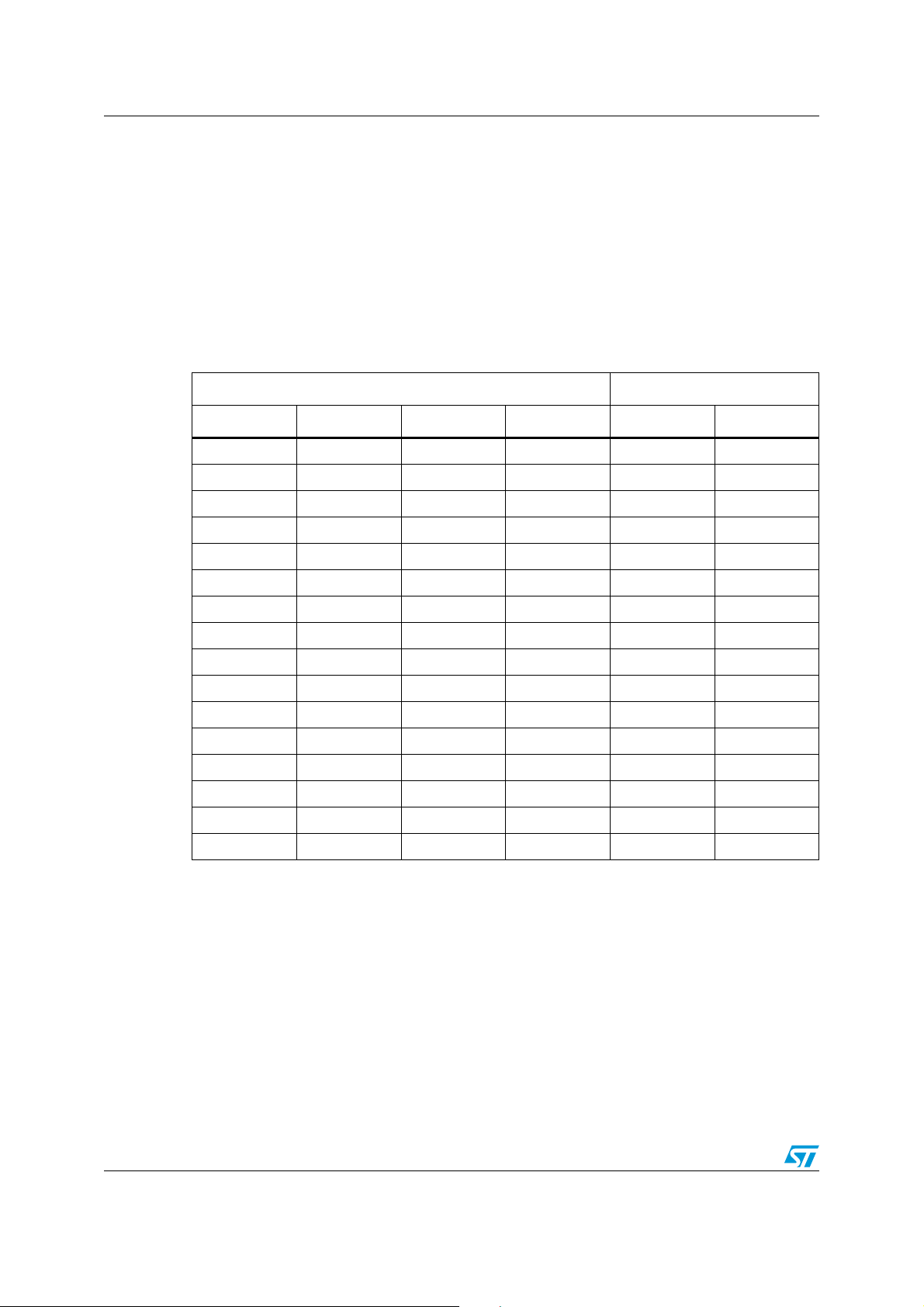
The M41T62/63/64 offers the user a programmable square wave function which is output on
the SQW pin. RS3-RS0 bits located in 04h establish the square wave output frequency.
These frequencies are listed in Tabl e 8 . Once the selection of the SQW frequency has been
completed, the SQW pin can be turned on and off under software control with the square
wave enable bit (SQWE) located in register 0Ah.
The SQW output is an N-channel, open drain output driver for the M41T64, and a full CMOS
output driver for the M41T62/63. The initial power-up default for the SQW output is 32 KHz
(except for M41T64, which defaults disabled).
Table 8. Square wave output frequency
Square wave bits Square wave
RS3 RS2 RS1 RS0 Frequency Units
0000None–
000132.768kHz
00108.192kHz
00114.096kHz
01002.048kHz
01011.024kHz
0110512Hz
0111256Hz
1000128Hz
100164Hz
101032Hz
101116Hz
11008Hz
11014Hz
11102Hz
11111Hz
3.7 Full-time 32 KHz square wave output (M41T64)
The M41T64 offers the user a special 32 KHz square wave function which is enabled on
power-up to output on the F
(ST bit = '0'). This function is available within one second (typ) of initial power-up and can
only be disabled by setting the 32KE bit to '0' or the ST bit to '1.' If not used, the F
should be disconnected and allowed to float.
pin as long as VCC ≥ 1.3 V, and the oscillator is running
32K
32K
pin
28/44 Doc ID 10397 Rev 19
Page 29

M41T62/63/64/65 Clock operation
3.8 Century bits
These two bits will increment in a binary fashion at the turn of the century, and handle all
leap years correctly. See Table 10 on page 30 for additional explanation.
3.9 Output driver pin (M41T62/65)
When the OFIE bit, AFE bit, and watchdog register are not set to generate an interrupt, the
IRQ
/OUT pin becomes an output driver that reflects the contents of D7 of the calibration
register. In other words, when D7 (OUT bit) is a '0,' then the IRQ
/OUT pin will be driven low.
Note: The IRQ
/OUT pin is an open drain which requires an external pull-up resistor.
3.10 Oscillator stop detection
If the oscillator fail (OF) bit is internally set to a '1,' this indicates that the oscillator has either
stopped, or was stopped for some period of time and can be used to judge the validity of the
clock and date data. This bit will be set to '1' any time the oscillator stops.
In the event the OF bit is found to be set to '1' at any time other than the initial power-up, the
STOP bit (ST) should be written to a '1,' then immediately reset to '0.' This will restart the
oscillator.
The following conditions can cause the OF bit to be set:
● The first time power is applied (defaults to a '1' on power-up).
Note: If the OF bit cannot be written to '0' four (4) seconds after the initial power-up, the STOP bit
(ST) should be written to a '1,' then immediately reset to '0.'
● The voltage present on V
● The ST bit is set to '1.'
● External interference of the crystal
If the oscillator fail interrupt enable bit (OFIE) is set to a '1,' the IRQ
The IRQ
register).
output is cleared by resetting the OFIE or OF bit to '0' (NOT by reading the flag
or battery is insufficient to support oscillation.
CC
pin will also be activated.
The OF bit will remain set to '1' until written to logic '0.' The oscillator must start and have
run for at least 4 seconds before attempting to reset the OF bit to '0.' If the trigger event
occurs during a power-down condition, this bit will be set correctly.
Doc ID 10397 Rev 19 29/44
Page 30
Clock operation M41T62/63/64/65
3.11 Initial power-on defaults
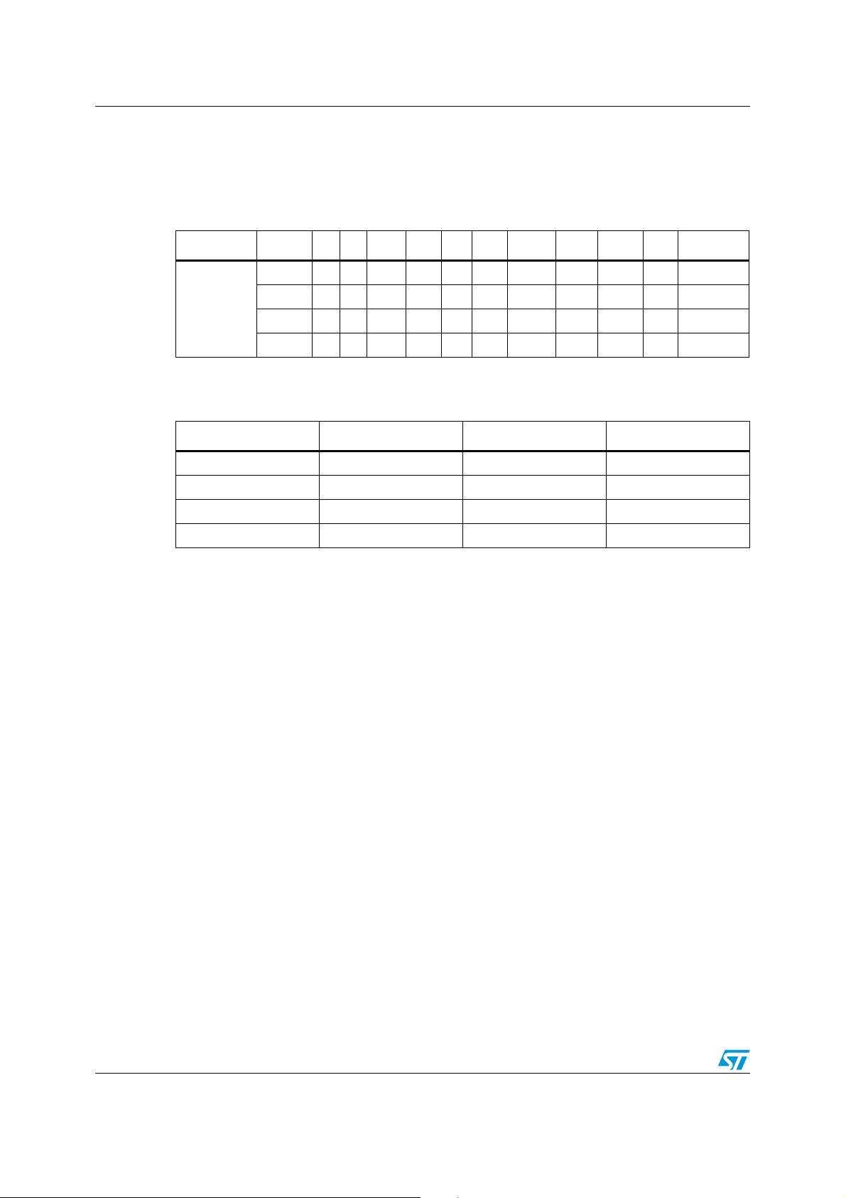
Upon application of power to the device, the register bits will initially power-on in the state
indicated in Ta bl e 9 .
Table 9. Initial power-on default values
Condition Device ST OF OFIE OUT FT AFE SQWE 32KE RS3-1 RS0 Watchdog
M41T62 0 1 0 1 N/A 0 1 N/A 0 1 0
Initial
power-up
1. All other control bits power up in an undetermined state.
Table 10. Century bits examples
M41T63 0 1 N/A N/A N/A N/A 1 N/A 0 1 0
(1)
M41T64 0 1 N/A N/A N/A N/A 0 1 0 1 0
M41T65 0 1 0 1 0 0 N/A N/A N/A N/A 0
CB0 CB1 Leap year? Example
(1)
00Yes2000
0 1 No 2100
1 0 No 2200
1 1 No 2300
1. Leap year occurs every four years (for years evenly divisible by four), except for years evenly divisible by
100. The only exceptions are those years evenly divisible by 400 (the year 2000 was a leap year, year
2100 is not).
30/44 Doc ID 10397 Rev 19
Page 31
M41T62/63/64/65 Maximum ratings
4 Maximum ratings
Stressing the device above the rating listed in the absolute maximum ratings table may
cause permanent damage to the device. These are stress ratings only and operation of the
device at these or any other conditions above those indicated in the operating sections of
this specification is not implied. Exposure to absolute maximum rating conditions for
extended periods may affect device reliability.
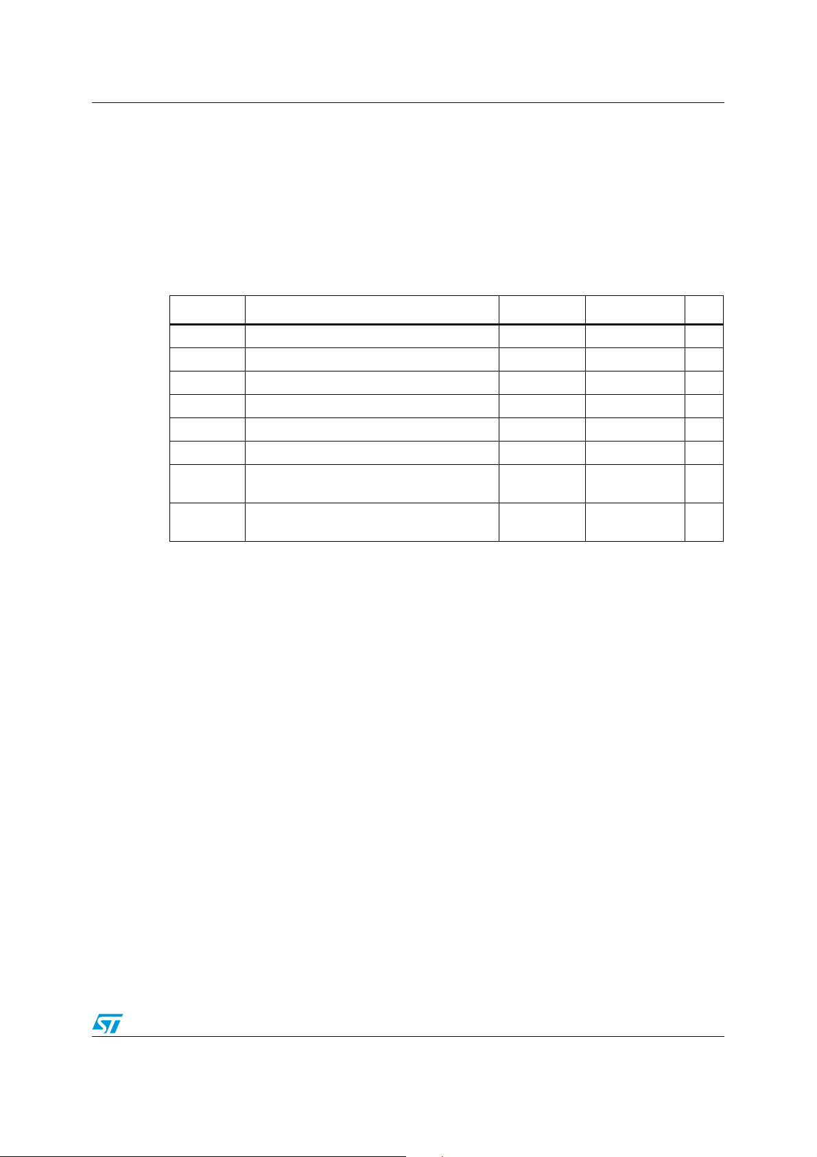
Table 11. Absolute maximum ratings
Sym Parameter Conditions
(1)
Val ue
(2)
Unit
T
STG
V
CC
T
SLD
V
IO
I
O
P
V
ESD(HBM)
V
ESD(RCDM)
1. Test conforms to JEDEC standard.
2. Data based on characterization results, not tested in production.
3. Reflow at peak temperature of 260 °C. The time above 255 °C must not exceed 30 seconds.
Storage temperature (VCC off, oscillator off) –55 to 125
Supply voltage –0.3 to 5.0 V
(3)
Lead solder temperature for 10 seconds 260 °C
Input or output voltages –0.2 to Vcc+0.3 V
Output current 20 mA
Power dissipation 1 W
D
Electro-static discharge voltage
(human body model)
Electro-static discharge voltage
(robotic charged device model)
= 25 °C >1500 V
T
A
T
= 25 °C >1000 V
A
°C
Doc ID 10397 Rev 19 31/44
Page 32
DC and AC parameters M41T62/63/64/65
5 DC and AC parameters
This section summarizes the operating and measurement conditions, as well as the DC and
AC characteristics of the device. The parameters in the following DC and AC characteristic
tables are derived from tests performed under the measurement conditions listed in the
relevant tables. Designers should check that the operating conditions in their projects match
the measurement conditions when using the quoted parameters.
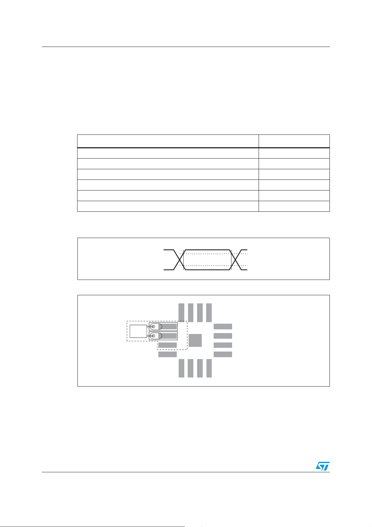
Table 12. Operating and AC measurement conditions
Parameter M41T6x
(1)
Supply voltage (V
Ambient operating temperature (T
Load capacitance (C
) 1.3 V to 4.4 V
CC
) –40 to 85 °C
A
) 50 pF
L
Input rise and fall times ≤ 5 ns
Input pulse voltages 0.2 VCC to 0.8 V
Input and output timing ref. voltages 0.3 VCC to 0.7 V
1. Output Hi-Z is defined as the point where data is no longer driven.
Figure 24. AC measurement I/O waveform
0.8V
0.2V
CC
CC
0.7V
0.3V
CC
CC
Figure 25. Crystal isolation example
Local Grounding Plane
(Layer 2)
Crystal
XI
XO
GND
CC
CC
AI02568
Note: Substrate pad should be tied to V
SS
.
32/44 Doc ID 10397 Rev 19
AI09127
Page 33
M41T62/63/64/65 DC and AC parameters
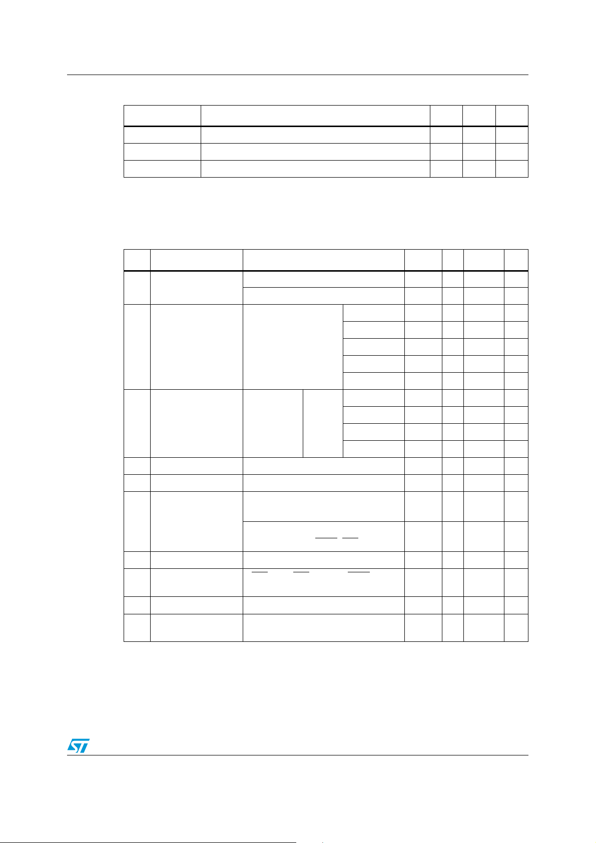
Table 13. Capacitance
Symbol Parameter
(1)(2)
Min Max Unit
C
IN
(3)
C
OUT
t
LP
1. Effective capacitance measured with power supply at 3.6 V; sampled only, not 100% tested.
2. At 25°C, f = 1 MHz.
3. Outputs deselected.
Table 14. DC characteristics
Sym Parameter Test condition
(2)
V
Operating voltage
CC
Input capacitance - 7 pF
Output capacitance - 10 pF
Low-pass filter input time constant (SDA and SCL) - 50 ns
(1)
Min Typ Max Unit
Clock 1.0 4.4 V
I2C bus (400 kHz) 1.3 4.4 V
4.4 V 100 µA
3.6 V 50 70 µA
Supply current
I
CC1
SCL = 400 kHz
(no load)
3.0 V 35 µA
2.5 V 30 µA
2.0 V 20 µA
4.4 V 950 nA
3.6 V 375 700 nA
3.0 V at 25 °C 350 nA
2.0 V at 25 °C 310 nA
Supply current
I
CC2
(standby)
SCL = 0 Hz
all inputs
– 0.2 V
≥ V
CC
≤ VSS + 0.2 V
SQW off
VILInput low voltage –0.2 0.3 V
Input high voltage 0.7 V
V
IH
= 4.4 V, IOL = 3.0 mA
V
CC
CC
(SDA)
Output low voltage
V
OL
Output high voltage VCC = 4.4 V, IOH = –1.0 mA (push-pull) 2.4 V
V
OH
Pull-up supply
IRQ
voltage (open drain)
Input leakage current 0 V ≤ V
I
LI
Output leakage
I
LO
current
1. Valid for ambient operating temperature: TA = –40 to 85 °C; VCC = 1.3 V to 4.4 V (except where noted).
2. Oscillator startup guaranteed at 1.5 V only.
= 4.4 V, IOL = 1.0 mA
V
CC
(SQW, WDO
, IRQ)
/OUT, IRQ/FT/OUT, WDO, SQW
(M41T64 only)
≤ V
IN
CC
0 V ≤ V
OUT
≤ V
CC
CC
VCC+0.3 V
0.4 V
0.4 V
4.4 V
±1 μA
±1 μA
Doc ID 10397 Rev 19 33/44
V
Page 34
DC and AC parameters M41T62/63/64/65
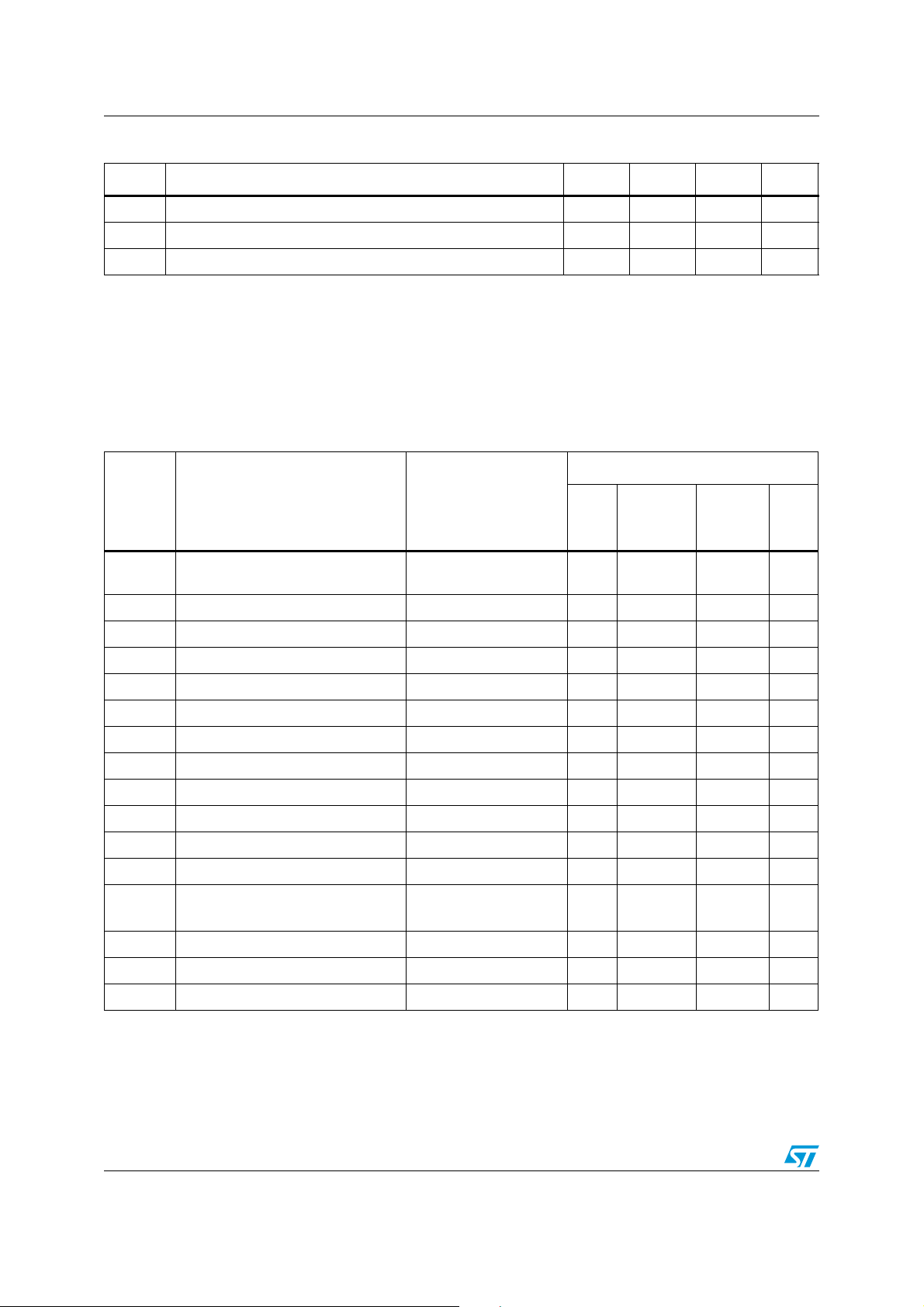
Table 15. Crystal electrical characteristics
Sym Parameter
f
O
R
S
C
L
1. For the QFN16 package, user-supplied external crystals are required. The 6 and 7 pF crystals listed in Table 16 below
have been evaluated by ST and have been found to be satisfactory for use with the M41T6x series RTC.
2. Load capacitors are integrated within the M41T6x. Circuit board layout considerations for the 32.768 kHz crystal of
minimum trace lengths and isolation from RF generating signals should be taken into account.
3. Guaranteed by design.
4. R
S (max)
(1)(2)
Min Typ Max Units
Resonant frequency - 32.768 kHz
Series resistance (TA = –40 to 70 °C, oscillator startup at 2.0 V) - 75
(3)(4)
Load capacitance - 6 pF
= 65 kΩ for TA = –40 to 85 °C and oscillator startup at 1.5 V.
Table 16. Crystals suitable for use with M41T6x series RTCs
Manufacturer’s specifications
Vendor Order number Package
Citizen CMJ206T-32.768KDZB-UB
8.3 x 2.5 mm
leaded SMT
ESR
max
Tem p.
range (°C)
50 kΩ –40/+85 ±20 ppm 6 pF
Rated
tolerance
at 25 °C
kΩ
Rated
load
cap.
Citizen CM315-32.768KDZY-UB 3.2 x 1.5 x 0.9 mm SMT 70 kΩ –40/+85 ±20 ppm 7 pF
Ecliptek E4WCDA06-32.768K 2.0 x 6.0 mm thru-hole 50 kΩ –10/+60 ±20 ppm 6 pF
Ecliptek E5WSDC 07 - 32.768K 7 x 1.5 x 1.4 mm SMT 65 kΩ –40/+85 ±20 ppm 7 pF
ECS ECS-.327-6-17X-TR 3.8 x 8.5 x 2.5 mm SMT 50 kΩ –40/+85 ±20 ppm 6 pF
ECS ECS-.327-7-34B-TR 3.2 x 1.5 x 0.9 mm SMT 70 kΩ –40/+85 ±20 ppm 7 pF
ECS ECS-.327-7-38-TR 7 x 1.5 x 1.4 mm SMT 65 kΩ –40/+85 ±20 ppm 7 pF
(1)
Epson MC-146 32.7680KA-AG: ROHS
7 x 1.5 x 1.4 mm SMT 65 kΩ –40/+85 ±20 ppm 7 pF
Fox 298LF-0.032768-19 1.5 x 5.0 mm thru-hole 50 kΩ –20/+60 ±20 ppm 6 pF
Fox 299LF-0.032768-37 2.0 x 6.0 mm thru-hole 50 kΩ –20/+60 ±20 ppm 6 pF
Fox 414LF-0.032768-12 3.8 x 8.5 x 2.5 mm SMT 50 kΩ –40/+85 ±20 ppm 6 pF
Fox 501LF-0.032768-5 7 x 1.5 x 1.4 mm SMT 65 kΩ –40/+85 ±20 ppm 7 pF
Micro
Crystal
MS3V-T1R 32.768KHZ 7PF 20PPM
6.7 x 1.4 mm
leaded SMT
65 kΩ –40/+85 ±20 ppm 7 pF
Pletronics SM20S - 32.768K - 6pF 3.8 x 8.5 x 2.5 mm SMT 50 kΩ –40/+85 ±20 ppm 6 pF
Seiko SSPT7F-7PF20PPM 7 x 1.5 x 1.4 mm SMT 65 kΩ –40/+85 ±20 ppm 7 pF
Seiko VT200F-6PF20PPM 2.0 x 6.0 mm thru-hole 50 kΩ –10/+60 ±20 ppm 6 pF
1. Epson MC-146 32.7680KA-E: ROHS is 6 pF version.
34/44 Doc ID 10397 Rev 19
Page 35
M41T62/63/64/65 DC and AC parameters
Table 17. Oscillator characteristics
Symbol Parameter Conditions Min Typ Max Unit
V
t
1. Reference value. TA = 25 °C, VCC = 3.0 V, CMJ-145 (CL = 6 pF, 32,768 Hz) manufactured by Citizen,
2. Devices in LCC8 package ((M41T62LC6F) are tested not to exceed ±20 ppm oscillator frequency error at
Oscillator start voltage ≤ 10 seconds 1.5 V
STA
Oscillator start time VCC = 3.0 V 1 s
STA
C
XIN capacitance 12 pF
g
XOUT capacitance 12 pF
C
d
IC-to-IC frequency variation
CL = Cg • Cd / (Cg + Cd).
25 °C, which equates to about 52 seconds per month.
(1)(2)
–10 +10 ppm
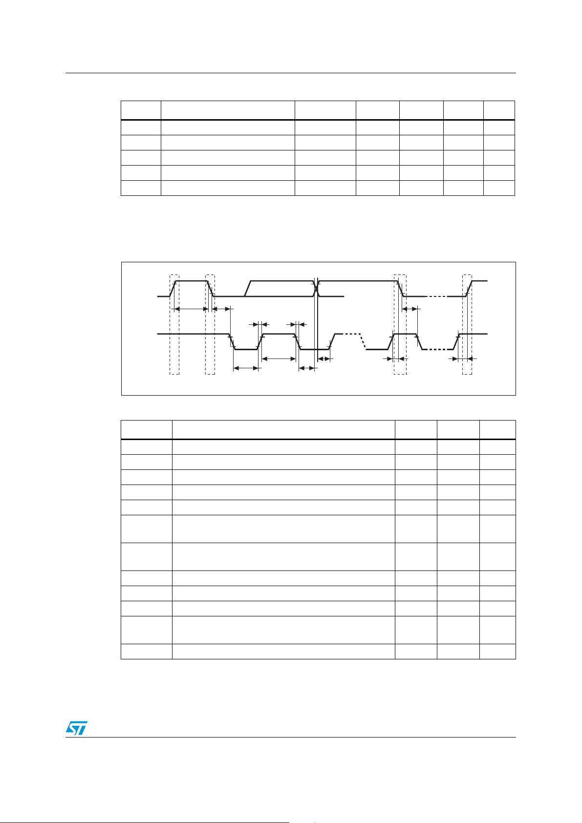
Figure 26. Bus timing requirements sequence
SDA
t
SU:STA
t
HD:STA
P
t
SU:STO
AI00589
SCL
t
BUF
t
HD:STA
t
HIGH
t
LOW
t
F
t
t
HD:DAT
SU:DAT
SR
t
R
SP
Table 18. AC characteristics
Sym Parameter
f
SCL
t
LOW
t
HIGH
t
R
t
F
t
HD:STA
t
SU:STA
t
SU:DAT
t
HD:DAT
t
SU:STO
t
BUF
t
rec
1. Valid for ambient operating temperature: TA = –40 to 85 °C; VCC = 1.3 to 4.4 V (except where noted).
2. Transmitter must internally provide a hold time to bridge the undefined region (300 ns max) of the falling
edge of SCL.
SCL clock frequency 0 400 kHz
Clock low period 1.3 µs
Clock high period 600 ns
SDA and SCL rise time 300 ns
SDA and SCL fall time 300 ns
START condition hold time
(after this period the first clock pulse is generated)
START condition setup time
(only relevant for a repeated start condition)
(2)
Data setup time 100 ns
Data hold time 0 µs
STOP condition setup time 600 ns
Time the bus must be free before a new
transmission can start
Watchdog output pulse width 96 98 ms
(1)
Min Max Units
600 ns
600 ns
1.3 µs
Doc ID 10397 Rev 19 35/44
Page 36

Package mechanical information M41T62/63/64/65
6 Package mechanical information
In order to meet environmental requirements, ST offers these devices in different grades of
ECOPACK
specifications, grade definitions and product status are available at: www.st.com.
ECOPACK
®
packages, depending on their level of environmental compliance. ECOPACK®
®
is an ST trademark.
36/44 Doc ID 10397 Rev 19
Page 37
M41T62/63/64/65 Package mechanical information
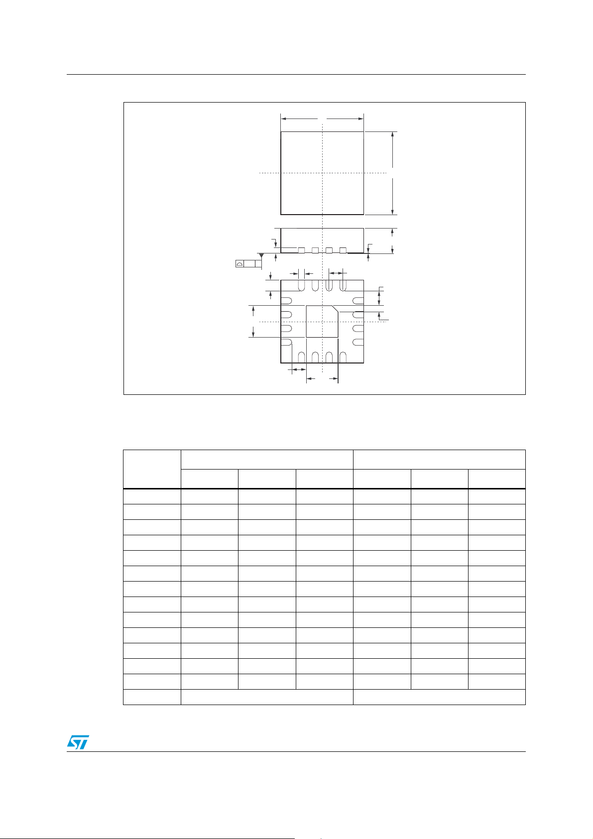
Figure 27. QFN16 – 16-pin, quad, flat package, no-lead, 3 mm x 3 mm body size, outline
D
E
Note: Drawing is not to scale.
Table 19. QFN16 – 16-pin, quad, flat package, no-lead, 3 mm x 3 mm body size,
mechanical data
Symb
Typ Min Max Typ Min Max
A 0.90 0.80 1.00 0.035 0.032 0.039
A1 0.02 0.00 0.05 0.001 0.000 0.002
A3 0.20 – – 0.008 – –
b 0.25 0.18 0.30 0.010 0.007 0.012
D 3.00 2.90 3.10 0.118 0.114 0.122
D2 1.70 1.55 1.80 0.067 0.061 0.071
E 3.00 2.90 3.10 0.118 0.114 0.122
E2 1.70 1.55 1.80 0.067 0.061 0.071
e0.50– –0.020– –
K0.20– –0.008– –
L 0.40 0.30 0.50 0.016 0.012 0.020
ddd – 0.08 – – 0.003 –
Ch – 0.33 – – 0.013 –
N16 16
ddd
E2
A3
C
b
L
K
D2
e
1
2
3
A1
A
K
Ch
mm inches
QFN16-A
Doc ID 10397 Rev 19 37/44
Page 38
Package mechanical information M41T62/63/64/65
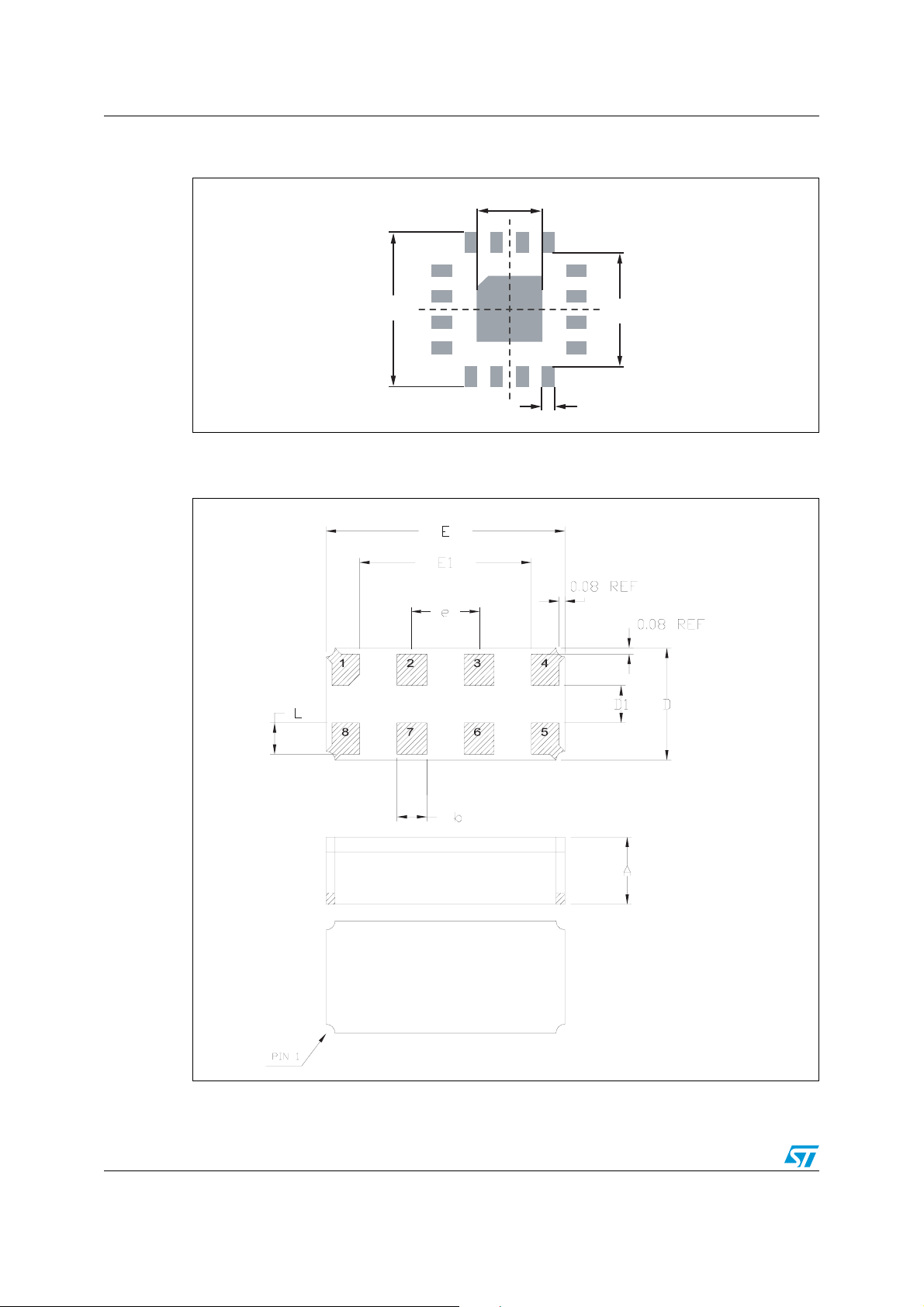
Figure 28. QFN16 – 16-pin, quad, flat package, no-lead, 3 x 3 mm, recommended
footprint
1.60
3.55
Note: Dimensions shown are in millimeters (mm).
Figure 29. LCC8 — 8-pin, 1.5 mm x 3.2 mm leadless chip carrier, outline
0.28
2.0
AI09126
bottom view
38/44 Doc ID 10397 Rev 19
side view
top view
8241725_A
Page 39
M41T62/63/64/65 Package mechanical information
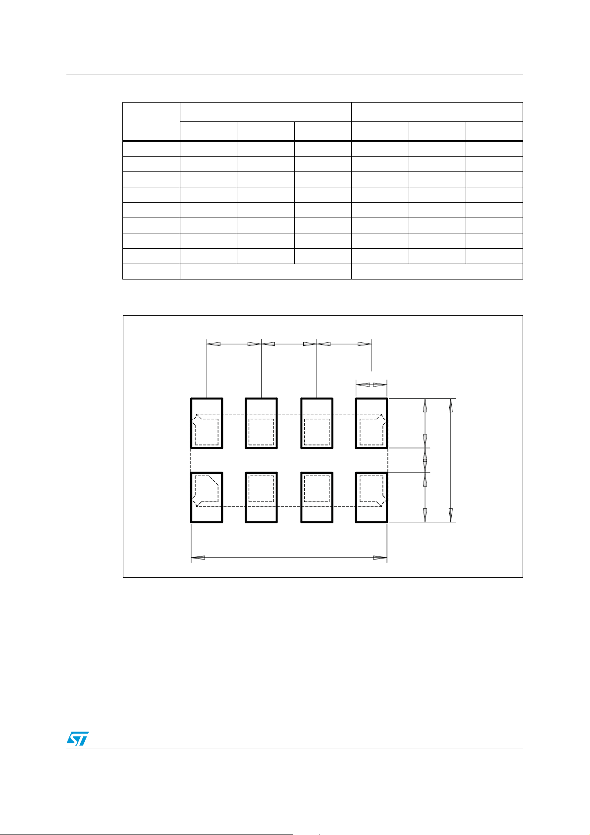
Table 20. LCC8 — 8-pin, 1.5 mm x 3.2 mm leadless chip carrier, mechanical data
Symb
Typ Min Max Typ Min Max
A0.800.031
b 0.30 0.40 0.50 0.012 0.016 0.020
D 1.40 1.50 1.60 0.055 0.059 0.063
D1 0.40 0.50 0.60 0.016 0.020 0.024
E 3.10 3.20 3.30 0.122 0.126 0.130
E1 2.20 2.30 2.40 0.087 0.091 0.094
e 0.90 0.035
L 0.32 0.42 0.52 0.013 0.017 0.020
N8 8
Figure 30. LCC8 — 8-pin, 1.5 mm x 3.2 mm leadless chip carrier, recommended
footprint
mm inches
0.9 0.9 0.9
0.5
3.2
Note: Dimensions shown are typical values, in millimeters (mm).
0.80.8 0.4
2.0
Doc ID 10397 Rev 19 39/44
Page 40
Package mechanical information M41T62/63/64/65
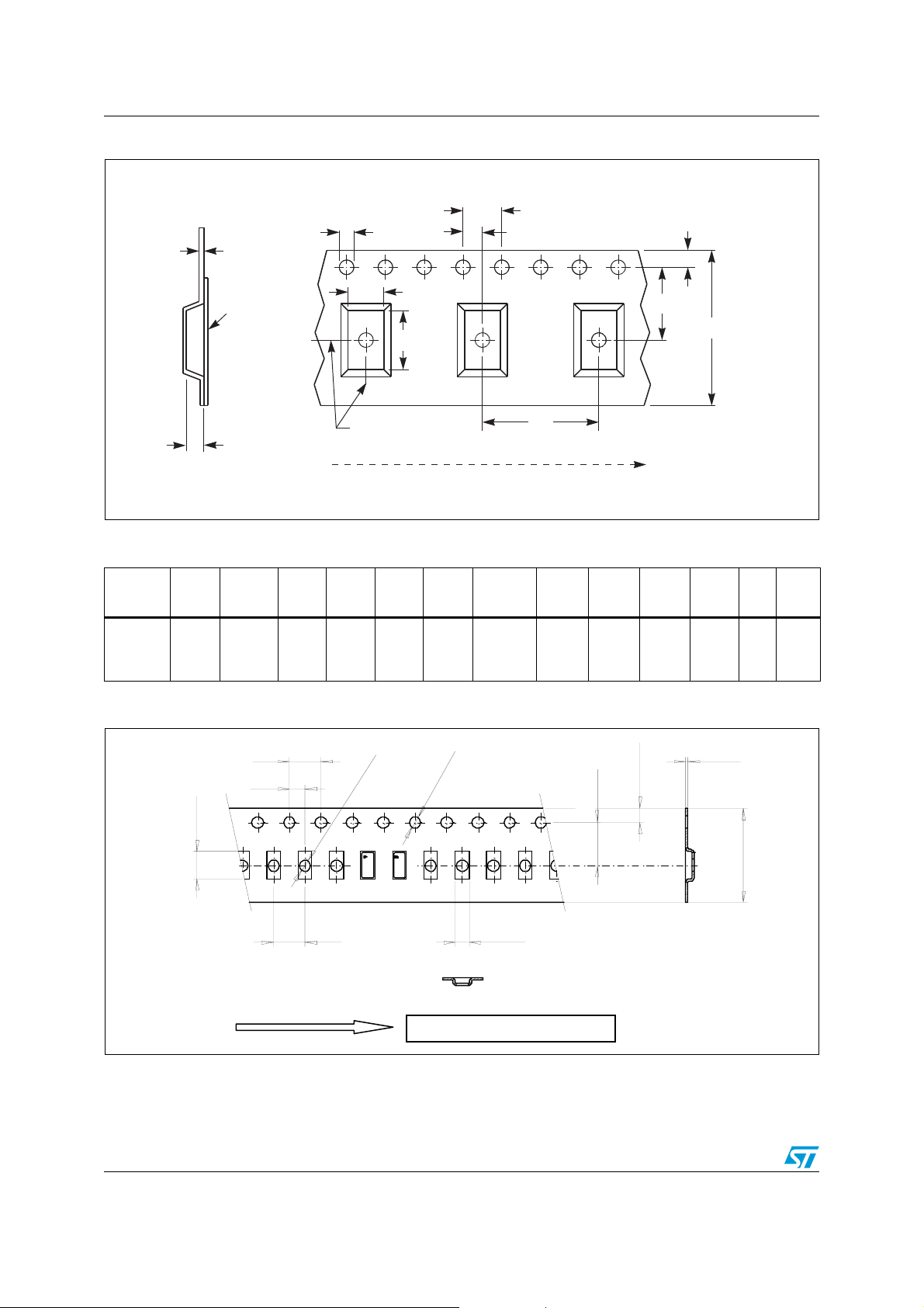
Figure 31. Carrier tape for QFN16 3 mm x 3 mm package
P
D
T
A
TOP COVER
TAPE
K
0
0
CENTER LINES
OF CAVITY
P
2
B
0
0
P
1
E
F
W
USER DIRECTION OF FEED
Table 21. Carrier tape dimensions for QFN16 3 mm x 3 mm package
Package W D E P
1.50
+0.10
/-0.00
1.75
±0.10
4.00
±0.10
QFN16
12.00
±0.30
P
0
2.00
±0.10
FA0B
2
5.50
±0.05
3.30
±0.10
0
3.30
±0.10
1.10
±0.10
Figure 32. Carrier tape for LCC8 1.5 mm x 3.2 mm package
Ø
1.
1
0.
±
5
±0.05
5.5
±0.1
4
±0.1
2
±0.1
Ø
1.
.1
0
±
5
3.4 5
7604
7604
AM03073v1
K
P
0
8.00
±0.10
±0.1
1
TUnit
0.30
±0.05
±0.02
0.3
Bulk
Qty
mm 3000
1.75
±0.2
12
±0.1
±0.1
1.7 54
User Direction of Feed
Note: Dimensions shown are in millimeters (mm).
40/44 Doc ID 10397 Rev 19
Page 41
M41T62/63/64/65 Package mechanical information
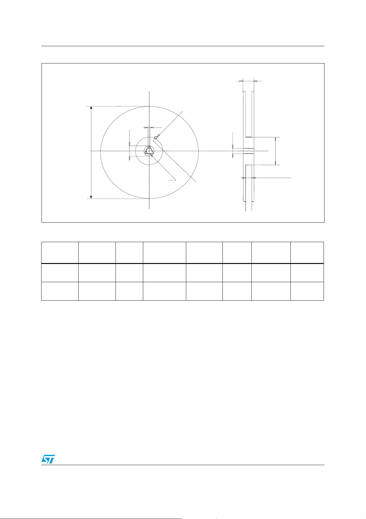
Figure 33. Reel schematic
T
40mm min.
Access hole
At slot location
B
D
C
A
Tape slot
Full ra dius
In core for
Tape s tart
2.5mm min.width
N
G measured
At hub
AM04928v1
Table 22. Reel dimensions for 12 mm carrier tape - QFN16 and LCC8 packages
Package
QFN16
LCC8
A
(max)
330 mm
(13-inch)
180 mm
(7-inch)
B
(min)
1.5 mm
1.5 mm
C
13 mm
± 0.2 mm
13 mm
± 0.2 mm
D
(min)
N
(min)
20.2 mm 60 mm
20.2 mm 60 mm
G
12.4 mm
+ 2/–0 mm
12.4 mm
+ 2/–0 mm
T
(max)
18.4 mm
18.4 mm
Note: The dimensions given in Ta bl e 2 2 incorporate tolerances that cover all variations on critical
parameters.
Doc ID 10397 Rev 19 41/44
Page 42

Part numbering M41T62/63/64/65
7 Part numbering
Table 23. Ordering information scheme
Example: M41T 62 Q 6 F
Device family
M41T
Device type and supply voltage
62 = V
63
64 = VCC = 1.3 V to 4.4 V
65 = VCC = 1.3 V to 4.4 V
Package
Q = QFN16 (3 mm x 3 mm)
LC = LCC8 (1.5 mm x 3.2 mm) (M41T62 only)
= 1.3 V to 4.4 V
CC
(1)
= VCC = 1.3 V to 4.4 V
Temperature range
6 = –40 °C to 85 °C
Shipping method
®
F = ECOPACK
1. Contact the ST sales office for availability.
package, tape & reel
For other options, or for more information on any aspect of this device, please contact the
ST sales office nearest you.
42/44 Doc ID 10397 Rev 19
Page 43
M41T62/63/64/65 Revision history
8 Revision history
Table 24. Document revision history
Date Revision Changes
26-Jan-2010 12
07-May-2010 13
25-May-2010 14
24-Mar-2011 15
22-Jun-2011 16 Updated Features; updated LCC8 package height in Figure 29.
10-Oct-2011 17
09-Nov-2011 18 Updated Figure 29, Ta b l e 2 2 ; added Ta bl e 2 0, Figure 30.
01-Dec-2011 19 Updated title and Ta b le 1 6 .
Minor textual changes; updated Section 3.2; footnote 3 in
Ta bl e 1 1 ; footnote 1 in Ta bl e 1 5 ; text in Section 6; Tab l e 1 6 , 18.
Updated title of datasheet, Features, Section 1, Section 3.1, 3.2,
3.4, 3.10, Section 4, Figure 23, Ta b le 1 6 ; added Figure 20, added
embedded crystal package LCC8 (updated Figure 1, 5, 29,
Ta bl e 2 3 ).
Removed LCC8 package option throughout document; removed
footnote from Tab l e 1 4 .
Updated Ta bl e 1 , 17, 23; added LCC8 package option throughout
datasheet; added tape and reel specifications for packages
(Figure 31, 32, 33, Ta b le 2 1 , 22).
Updated V
textual updates.
test condition in Table 14: DC characteristics; minor
OL
Doc ID 10397 Rev 19 43/44
Page 44

M41T62/63/64/65
Please Read Carefully:
Information in this document is provided solely in connection with ST products. STMicroelectronics NV and its subsidiaries (“ST”) reserve the
right to make changes, corrections, modifications or improvements, to this document, and the products and services described herein at any
time, without notice.
All ST products are sold pursuant to ST’s terms and conditions of sale.
Purchasers are solely responsible for the choice, selection and use of the ST products and services described herein, and ST assumes no
liability whatsoever relating to the choice, selection or use of the ST products and services described herein.
No license, express or implied, by estoppel or otherwise, to any intellectual property rights is granted under this document. If any part of this
document refers to any third party products or services it shall not be deemed a license grant by ST for the use of such third party products
or services, or any intellectual property contained therein or considered as a warranty covering the use in any manner whatsoever of such
third party products or services or any intellectual property contained therein.
UNLESS OTHERWISE SET FORTH IN ST’S TERMS AND CONDITIONS OF SALE ST DISCLAIMS ANY EXPRESS OR IMPLIED
WARRANTY WITH RESPECT TO THE USE AND/OR SALE OF ST PRODUCTS INCLUDING WITHOUT LIMITATION IMPLIED
WARRANTIES OF MERCHANTABILITY, FITNESS FOR A PARTICULAR PURPOSE (AND THEIR EQUIVALENTS UNDER THE LAWS
OF ANY JURISDICTION), OR INFRINGEMENT OF ANY PATENT, COPYRIGHT OR OTHER INTELLECTUAL PROPERTY RIGHT.
UNLESS EXPRESSLY APPROVED IN WRITING BY TWO AUTHORIZED ST REPRESENTATIVES, ST PRODUCTS ARE NOT
RECOMMENDED, AUTHORIZED OR WARRANTED FOR USE IN MILITARY, AIR CRAFT, SPACE, LIFE SAVING, OR LIFE SUSTAINING
APPLICATIONS, NOR IN PRODUCTS OR SYSTEMS WHERE FAILURE OR MALFUNCTION MAY RESULT IN PERSONAL INJURY,
DEATH, OR SEVERE PROPERTY OR ENVIRONMENTAL DAMAGE. ST PRODUCTS WHICH ARE NOT SPECIFIED AS "AUTOMOTIVE
GRADE" MAY ONLY BE USED IN AUTOMOTIVE APPLICATIONS AT USER’S OWN RISK.
Resale of ST products with provisions different from the statements and/or technical features set forth in this document shall immediately void
any warranty granted by ST for the ST product or service described herein and shall not create or extend in any manner whatsoever, any
liability of ST.
ST and the ST logo are trademarks or registered trademarks of ST in various countries.
Information in this document supersedes and replaces all information previously supplied.
The ST logo is a registered trademark of STMicroelectronics. All other names are the property of their respective owners.
© 2011 STMicroelectronics - All rights reserved
STMicroelectronics group of companies
Australia - Belgium - Brazil - Canada - China - Czech Republic - Finland - France - Germany - Hong Kong - India - Israel - Italy - Japan -
Malaysia - Malta - Morocco - Philippines - Singapore - Spain - Sweden - Switzerland - United Kingdom - United States of America
www.st.com
44/44 Doc ID 10397 Rev 19
 Loading...