

Page 1
4 Mbit (512Kb x8 or 256Kb x16, Boot Block)
Low Voltage Single Supply Flash Memory
M29W400Tand M29W400Bare replaced
respectivelyby theM29W400BT and
M29W400BB
2.7Vto 3.6V SUPPLYVOLTAGE for
PROGRAM,ERASE and READ OPERATIONS
FASTACCESSTIME:90ns
FASTPROGRAMMINGTIME
–10µs by Byte /16µs by Word typical
PROGRAM/ERASECONTROLLER(P/E.C.)
– Program Byte-by-Byte or Word-by-Word
– Status Register bits andReady/BusyOutput
MEMORYBLOCKS
– Boot Block(Top or Bottom location)
– Parameter and Main blocks
BLOCK,MULTI-BLOCK and CHIP ERASE
MULTI BLOCKPROTECTION/TEMPORARY
UNPROTECTION MODES
ERASESUSPENDand RESUME MODES
– Read and Programanother Block during
EraseSuspend
LOWPOWER CONSUMPTION
– Stand-by and AutomaticStand-by
100,000PROGRAM/ERASECYCLES per
BLOCK
20YEARSDATARETENTION
– Defectivity below 1ppm/year
ELECTRONICSIGNATURE
– ManufacturerCode: 0020h
– Device Code, M29W400T:00EEh
– Device Code, M29W400B: 00EFh
DESCRIPTION
The M29W400 is a non-volatilememory that may
be erasedelectricallyat theblock or chipleveland
programmedin-systemon a Byte-by-ByteorWordby-Wordbasisusing onlya single2.7Vto3.6V V
supply. For Program and Erase operations the
necessary high voltages are generated internally.
The device can also be programmed in standard
programmers.
The arraymatrixorganisationallowseach block to
be erased and reprogrammed without affecting
other blocks. Blockscan be protectedagainstprograming and erase on programming equipment,
CC
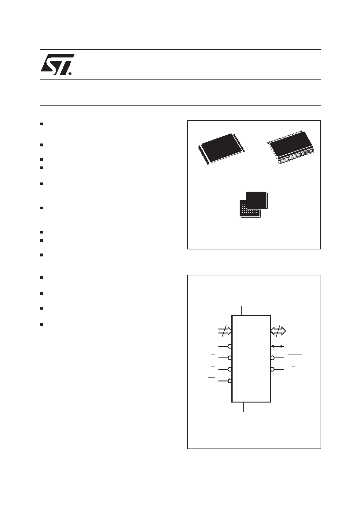
12 x 20 mm
BGA
FBGA48 (ZA)
8 x 6 solder balls
Figure 1. LogicDiagram
V
CC
18
A0-A17
W
E
G
RP
M29W400T
M29W400B
V
SS
M29W400T
M29W400B
NOT FOR NEW DESIGN
44
1
SO44 (M)TSOP48 (N)
15
DQ0-DQ14
DQ15A–1
BYTE
RB
AI02065
November 1999 1/34
This isinformationona product stillin productionbut not recommendedfor newdesigns.
Page 2
M29W400T, M29W400B
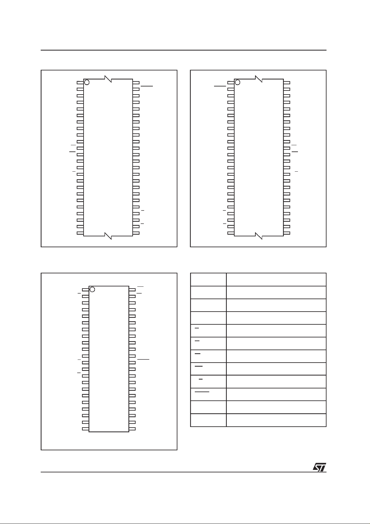
Figure 2A. TSOP Pin Connections
A15
1
A14
A13
A12
A11
A10 DQ14
A9
A8
NC
NC
W
RP
NC
NC
RB
NC
A17
A7
A6
A5
A4
A3
A2
A1
M29W400T
12
M29W400B
13
(Normal)
24 25
48
37
36
AI02066
A16
BYTE
V
SS
DQ15A–1
DQ7
DQ6
DQ13
DQ5
DQ12
DQ4
V
CC
DQ11
DQ3
DQ10
DQ2
DQ9
DQ1
DQ8
DQ0
G
V
SS
E
A0
Figure 2B. TSOP ReversePin Connections
A16
BYTE
V
SS
DQ15A–1
DQ7
DQ14
DQ6
DQ13
DQ5
DQ12
DQ4
V
CC
DQ11
DQ3
DQ10
DQ2
DQ9
DQ1
DQ8
DQ0
V
SS
A0
1
M29W400T
12
M29W400B
13
(Reverse)
G
E
24 25
AI02067
48
37
36
A15
A14
A13
A12
A11
A10
A9
A8
NC
NC
W
RP
NC
NC
RB
NC
A17
A7
A6
A5
A4
A3
A2
A1
Warning: NC = Not Connected. Warning: NC = Not Connected.
Figure 2C. SO Pin Connections
Table1. Signal Names
A0-A17 Address Inputs
NC RP
1
2
3
A17 A8
A7
4
5
A6
6
A5
A4
7
A3
8
A2
9
A1
10
A0
11
M29W400T
M29W400B
12
13
14
15
16
17DQ1
18
19
20
21
V
SS
DQ0
DQ8
DQ9
DQ10
DQ3
DQ11
E
G
44
43
42
41
40
39
38
37
36
35
34
33
32
31
30
29
28
27
26
25
24
2322
AI02068
WRB
A9
A10
A11
A12
A13
A14
A15
A16
BYTE
V
SS
DQ15A–1
DQ7
DQ14
DQ6
DQ13
DQ5DQ2
DQ12
DQ4
V
CC
DQ0-DQ7 Data Input/Outputs,Command Inputs
DQ8-DQ14 Data Input/Outputs
DQ15A–1 Data Input/Outputor Address Input
E Chip Enable
G Output Enable
W Write Enable
RP Reset /Block TemporaryUnprotect
RB Ready/Busy Output
BYTE Byte/Word Organisation
V
CC
V
SS
Supply Voltage
Ground
Warning: NC = Not Connected.
2/34
Page 3
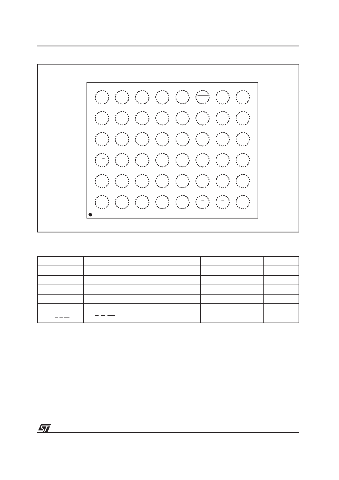
Figure 2D. FBGA Package Ball Out (Top View)
M29W400T, M29W400B
87654321
F
E
D
C
B
A
A4A3
Warning: NC = Not Connected.
Table2. AbsoluteMaximumRatings
A15A14A12A13
A11 DQ7
NC
A2 V
(1)
A5
A1
A16
DQ2
BYTE
DQ12DQ5NCNCRPW
DQ15
A–1
CC
GEA0
V
SS
DQ6DQ13DQ14A10A8A9
DQ4V
DQ3DQ11DQ10NCNCRB
DQ1DQ9DQ8DQ0A6A17A7
SS
AI00912
Symbol Parameter Value Unit
T
A
T
BIAS
T
STG
(2)
V
IO
V
CC
V
(A9, E, G, RP)
Notes: 1. Except for the rating ”Operating TemperatureRange”, stresses above those listedin theTable ”Absolute Maximum Ratings”
may cause permanent damage to the device. These are stress ratings only and operationof the device atthese or any other
conditions above those indicated in the Operating sections of this specification is notimplied. Exposure to AbsoluteMaximum
Rating conditions for extended periods may affect device reliability. Referalso to the STMicroelectronics SURE Program and other
relevant qualitydocuments.
2. Minimum Voltagemay undershootto–2V duringtransition and for less than 20ns.
3. Depends on range.
Ambient Operating Temperature
TemperatureUnder Bias –50 to125 °C
Storage Temperature –65 to150 °C
Input or OutputVoltages –0.6 to 5 V
Supply Voltage –0.6 to 5 V
(2)
A9, E, G, RP Voltage –0.6to 13.5 V
DESCRIPTION(Cont’d)
and temporarily unprotected to make changes in
the application. Each block can be programmed
and erasedover 100,000 cycles.
Instructions for Read/Reset,Auto Selectfor reading the Electronic Signature or Block Protection
(3)
–40 to85 °C
Suspend and Resumeare writtento the devicein
cyclesofcommandstoa CommandInterfaceusing
standardmicroprocessor write timings.
The device is offered in TSOP48 (12 x 20mm),
SO44 and FBGA48 (8 x 6 balls, 0.8mm pitch)
packages. Both normal and reverse pinouts are
availablefor the TSOP48 package.
status,Programming,BlockandChipErase,Erase
3/34
Page 4
M29W400T, M29W400B
Figure 3. MemoryMap and Block Address Table(x8)
7FFFFh
7C000h
7BFFFh
7A000h
79FFFh
78000h
77FFFh
70000h
6FFFFh
60000h
5FFFFh
50000h
4FFFFh
40000h
3FFFFh
30000h
2FFFFh
20000h
1FFFFh
10000h
0FFFFh
00000h
M29W400T
16K BOOT BLOCK
8K PARAMETER BLOCK
8K PARAMETER BLOCK
32K MAIN BLOCK
64K MAIN BLOCK
64K MAIN BLOCK
64K MAIN BLOCK
64K MAIN BLOCK
64K MAIN BLOCK
64K MAIN BLOCK
64K MAIN BLOCK
7FFFFh
70000h
6FFFFh
60000h
5FFFFh
50000h
4FFFFh
40000h
3FFFFh
30000h
2FFFFh
20000h
1FFFFh
10000h
0FFFFh
08000h
07FFFh
06000h
05FFFh
04000h
03FFFh
00000h
M29W400B
64K MAIN BLOCK
64K MAIN BLOCK
64K MAIN BLOCK
64K MAIN BLOCK
64K MAIN BLOCK
64K MAIN BLOCK
64K MAIN BLOCK
32K MAIN BLOCK
8K PARAMETER BLOCK
8K PARAMETER BLOCK
16K BOOT BLOCK
AI02090
Organisation
The M29W400 is organised as 512K x8 or 256K
x16 bits selectable by the BYTE signal. When
BYTE is Low the Byte-wide x8 organisation is
selected and the address lines are DQ15A–1 and
A0-A17. The Data Input/Output signal DQ15A–1
actsasaddresslineA–1 whichselectstheloweror
upper Byte of the memory word for output on
DQ0-DQ7,DQ8-DQ14remainat High impedance.
When BYTEis Highthe memory usestheaddress
inputs A0-A17 and the Data Input/Outputs DQ0DQ15.Memorycontrol is provided by ChipEnable
E, Output Enable G andWrite Enable W inputs.
AReset/BlockTemporaryUnprotection RPtri-level
input providesa hardware reset when pulled Low,
andwhenheld High(atV
) temporarily unprotects
ID
blocks previously protected allowing them to be
programedanderased.Erase andProgramoperations are controlled by an internal Program/Erase
Controller(P/E.C.).StatusRegisterdataoutput on
DQ7 providesa DataPolling signal,and DQ6and
DQ2 provideTogglesignalstoindicatethe state of
the P/E.C operations. A Ready/Busy RB output
indicatesthe completion of the internalalgorithms.
4/34
MemoryBlocks
The devices featureasymmetrically blockedarchitectureprovidingsystem memoryintegration.Both
M29W400Tand M29W400Bdeviceshaveanarray
of 11 blocks, one Boot Block of 16 KBytes or 8
KWords, two Parameter Blocks of 8 KBytes or 4
KWords, one Main Block of 32 KBytes or 16
KWordsand sevenMainBlocksof64KBytesor32
KWords.TheM29W400Thasthe BootBlockatthe
top of the memory ad dress spa ce and the
M29W400B locates the Boot Block startingat the
bottom. The memory maps are showed in Figure
3. Each block can beerased separately,any combination of blocks can be specifiedfor multi-block
eraseor the entirechip may be erased. The Erase
operations are managed automatically by the
P/E.C. The block erase operation can be suspended in order to read from or program to any
blocknot beingersased, and then resumed.
Block protection provides additional data security.
Each block can be separatelyprotected or unprotected against Program or Eraseon programming
equipment. All previously protected blocks can be
temporarilyunprotected in theapplication.
Page 5
M29W400T, M29W400B
Table3A. M29W400TBlock Address Table
Address Range (x8) Address Range(x16) A17 A16 A15 A14 A13 A12
00000h-0FFFFh 00000h-07FFFh 0 0 0 X X X
10000h-1FFFFh 08000h-0FFFFh 0 0 1 X X X
20000h-2FFFFh 10000h-17FFFh 0 1 0 X X X
30000h-3FFFFh 18000h-1FFFFh 0 1 1 X X X
40000h-4FFFFh 20000h-27FFFh 1 0 0 X X X
50000h-5FFFFh 28000h-2FFFFh 1 0 1 X X X
60000h-6FFFFh 30000h-37FFFh 1 1 0 X X X
70000h-77FFFh 38000h-3BFFFh 1110XX
78000h-79FFFh 3C000h-3CFFFh 111100
7A000h-7BFFFh 3D000h-3DFFFh 111101
7C000h-7FFFFh 3E000h-3FFFFh 11111X
Table3B. M29W400BBlock AddressTable
Address Range (x8) Address Range(x16) A17 A16 A15 A14 A13 A12
00000h-03FFFh 00000h-01FFFh 00000X
04000h-05FFFh 02000h-02FFFh 000010
06000h-07FFFh 03000h-03FFFh 000011
08000h-0FFFFh 04000h-07FFFh 0001XX
10000h-1FFFFh 08000h-0FFFFh 0 0 1 X X X
20000h-2FFFFh 10000h-17FFFh 0 1 0 X X X
30000h-3FFFFh 18000h-1FFFFh 0 1 1 X X X
40000h-4FFFFh 20000h-27FFFh 1 0 0 X X X
50000h-5FFFFh 28000h-2FFFFh 1 0 1 X X X
60000h-6FFFFh 30000h-37FFFh 1 1 0 X X X
70000h-7FFFFh 38000h-3FFFFh 1 1 1 X X X
Bus Operations
The following operations can be performed using
the appropriatebuscycles:Read (Array, Electronic
Signature, Block Protection Status), Write com-
mand,Output Disable, Standby,Reset, BlockProtection, Unprotection, Protection Verify, Unprotection VerifyandBlockTemporaryUnprotection.See
Tables4 and 5.
5/34
Page 6

M29W400T, M29W400B
Command Interface
Instructions,made up of commandswritten in cycles, canbe giventotheProgram/EraseController
through a Command Interface (C.I.). For added
data protection,program or eraseexecutionstarts
after4or6cycles.Thefirst,second,fourthandfifth
cycles are used to input Coded cycles to the C.I.
This Coded sequence is the same for all Program/Erase Controller instructions. The ’Command’itself and its confirmation,when applicable,
are givenon the third,fourth or sixth cycles. Any
incorrectcommand orany improper command sequence will reset the device to ReadArray mode.
Instructions
Seven instructions are defined to perform Read
Array,AutoSelect(toreadtheElectronicSignature
or BlockProtectionStatus),Program, BlockErase,
Chip Erase, Erase Suspend and Erase Resume.
The internal P/E.C. automaticallyhandles all timing and verification of the Program and Erase
operations.The Status RegisterData Polling,Toggle, Error bits and the RB output may be read at
any time, duringprogrammingor erase,tomonitor
the progress of the operation.
Instructionsare composed of upto sixcycles. The
first two cycles input a Coded sequence to the
CommandInterfacewhichis commontoallinstructions (see Table 8). The third cycle inputs the
instruction set-up command. Subsequent cycles
output theaddressed data,ElectronicSignatureor
Block Protection Status for Read operations. In
ordertogiveadditionaldataprotection,the instructions for Program and Block or Chip Erase require
furthercommandinputs.ForaPrograminstruction,
the fourth command cycle inputs the address and
data to be programmed. For an Erase instruction
(Block or Chip), the fourth and fifth cycles input a
further Coded sequence before the Eraseconfirm
commandon thesixthcycle. Erasureof a memory
blockmaybe suspended,in ordertoreaddatafrom
another block or to programdata in another block,
and thenresumed.
When power is first applied or if V
, the command interface is reset to Read
V
LKO
falls below
CC
Array.
SIGNALDESCRIPTIONS
See Figure 1 andTable1.
AddressInputs (A0-A17). The addressinputs for
the memoryarrayare latchedduringawriteoperation on the falling edge of Chip Enable E or Write
Enable W. InWord-wide organisationthe address
lines are A0-A17, in Byte-wide organisation
DQ15A–1acts as an additional LSB addressline.
WhenA9 is raised to V
, either a ReadElectronic
ID
Signature Manufacturer or Device Code, Block
Protection Status or a Write Block Protection or
Block Unprotection is enabled depending on the
combinationoflevelson A0,A1, A6, A12 andA15.
Data Input/Outputs (DQ0-DQ7). These Inputs/Outputsare used in the Byte-wideand Wordwide organisations. The input is data to be
programmed in the memory array or a command
to be written to the C.I. Both are latched on the
rising edge of Chip Enable E or Write Enable W.
The output is data from the Memory Array, the
Electronic Signature Manufacturer or Device
codes, the Block Protection Status or the Status
registerData Pollingbit DQ7,the Toggle Bits DQ6
and DQ2, the Errorbit DQ5or the EraseTimer bit
DQ3. Outputs are valid when Chip Enable E and
Output Enable G are active. The output is high
impedance when the chip is deselected or the
outputsaredisabledandwhen RPisat aLowlevel.
Data Input/Outputs (DQ8-DQ14 and DQ15A–1).
These Inputs/Outputsare additionallyused in the
Word-wideorganisation.WhenBYTEisHighDQ8DQ14 and DQ15A–1 act as the MSB of the Data
Inputor Output, functioningas describedfor DQ0DQ7 above, and DQ8-DQ15 are ’don’t care’ for
commandinputsor status outputs.When BYTEis
Low,DQ8-DQ14are highimpedance,DQ15A–1is
the AddressA–1 input.
Chip Enable (E). The Chip Enableinput activates
the memory control logic, input buffers, decoders
andsenseamplifiers.EHighdeselectsthememory
andreducesthepowerconsumptiontothestandby
level. E can also be used to controlwriting to the
commandregister and to thememory array, while
Wremainsata lowlevel.TheChipEnablemust be
forcedto V
duringthe BlockUnprotectionopera-
ID
tion.
6/34
Page 7

M29W400T, M29W400B
Output Enable (G). The Output Enable gates the
outputs through the data buffers during a read
operation. When G is High the outputs are High
impedance. G must be forced to V
level during
ID
Block Protection andUnprotectionoperations.
WriteEnable(W). Thisinput controlswriting tothe
CommandRegisterandAddressandDatalatches.
Byte/Word Organization Select (BYTE). The
BYTEinputselects theoutput configurationforthe
device: Byte-wide (x8) mode or Word-wide (x16)
mode. When BYTEis Low,the Byte-widemode is
selectedand the data is read and programmedon
DQ0-DQ7. In this mode, DQ8-DQ14 are at high
impedance and DQ15A–1 is the LSB address.
When BYTE is High, the Word-wide mode is selected and the data is read and programmed on
DQ0-DQ15.
Ready/Busy Output (RB). Ready/Busy is an
open-drainoutputandgivestheinternalstateofthe
P/E.C. of the device. When RB is Low, the device
is Busy with a Programor Erase operation and it
will not accept any additional program or erase
instructionsexcept the Erase Suspendinstruction.
WhenRB isHigh,thedeviceisreadyforanyRead,
Program or Erase operation. The RB will also be
High when the memoryis putin EraseSuspendor
Standby modes.
Reset/Block Temporary Unprotect Input (RP).
The RP Input provides hardware reset and protected block(s) temporary unprotection functions.
Reset of the memory is acheivedby pulling RPto
for atleastt
V
IL
.When thereset pulseis given,
PLPX
if the memory is in Read or Standby modes, it will
be available for new operations in t
PHEL
after the
rising edgeofRP.Ifthememoryis in Erase,Erase
Suspend or Program modes the reset will take
duringwhichtheRB signal will beheldatVIL.
t
PLYH
The end of the memory reset will be indicated by
the rising edge of RB. Ahardwareresetduring an
Erase or Program operation will corrupt the data
being programmed or the sector(s) being erased
(see Table14 andFigure9).
Temporary block unprotectionis made by holding
RP at V
. In this condition previously protected
ID
blocks can be programmedor erased.The transitionof RPfromV
When RP is returned from V
toVIDmustslower thant
IH
to VIHall blocks
ID
PHPHH
temporarily unprotected will be again protected.
See Table15 andFigure9.
V
Supply Voltage. The power supply for all
CC
operations (Read,Programand Erase).
Ground. VSSis the reference for all voltage
V
SS
measurements.
DEVICEOPERATIONS
See Tables 4, 5and 6.
Read. Read operations are used to output the
contents of the MemoryArray, the ElectronicSignature,the StatusRegister orthe BlockProtection
Status. Both Chip Enable E and Output Enable G
must be low in order to read the output of the
memory.
Write.Writeoperationsareused togiveInstruction
Commandsto thememory orto latchinputdatato
beprogrammed.Awriteoperationis initiatedwhen
Chip Enable E is Lowand Write Enable W is Low
withOutput EnableGHigh.Addressesare latched
onthefallingedgeof Wor E whicheveroccurslast.
CommandsandInputDataarelatchedontherising
edge of W orE whichever occursfirst.
OutputDisable. Thedata outputsare highimpedance whenthe OutputEnable G isHigh with Write
EnableW High.
Standby. The memory is in standby when Chip
EnableEis Highand theP/E.C. is idle.The power
consumption is reduced to the standby level and
the outputs are high impedance, independentof
the Output Enable G or Write EnableWinputs.
Automatic Standby. After 150ns of bus inactivity
and whenCMOSlevels are driving theaddresses,
the chip automatically enters a pseudo-standby
modewhere consumptionisreducedto the CMOS
standbyvalue, whileoutputs still drivethe bus.
Electronic Signature. Two codes identifyingthe
manufacturer andthedevicecanberead fromthe
memory. The manufacturer’s code for STMicroelectronics is 20h, the device code is EEh for
the M29W400T (Top Boot) and EFh for the
M29W400B(BottomBoot).Thesecodesallowprogramming equipment or applications to automaticallymatch their interfaceto thecharacteristicsof
the M29W400. The ElectronicSignature is output
by a Read operationwhen the voltage applied to
A9 is at V
and address inputs A1 is Low. The
ID
manufacturer code is output when the Address
input A0 is Low and the device code when this
input is High. Other Address inputs are ignored.
The codesare output on DQ0-DQ7.
.
TheElectronicSignaturecan also beread,without
raisingA9toV
, by givingthe memorythe Instruc-
ID
tion AS. If the Byte-wide configuration is selected
thecodesareoutputon DQ0-DQ7withDQ8-DQ14
at High impedance; if the Word-wideconfiguration
is selectedthe codes are outputon DQ0-DQ7with
DQ8-DQ15at 00h.
7/34
Page 8
M29W400T, M29W400B
Table4. User Bus Operations
(1)
Operation E G W RP BYTE A0 A1 A6 A9 A12 A15
V
V
V
Read Word V
Read Byte V
Write Word V
Write Byte V
OutputDisable V
Standby V
ILVIL
ILVIL
ILVIH
ILVIH
ILVIH
XXVIHX X X X X X X Hi-Z Hi-Z Hi-Z
IH
IH
V
IH
V
IL
V
IL
V
IH
Reset X X X V
Block
Protection
Blocks
Unprotection
Block
Protection
Verify
Block
Unprotection
Verify
Block
Temporary
Unprotection
Notes: 1. X = V
(2,4)
(2,4)
(2,4) V
ILVIDVIL
VIDVIDVILPulse V
(4)
VILV
VILV
Pulse V
V
IL
IH
V
IL
IH
XX X V
orV
IL
2. Block Address must be given on A12-A17 bits.
3. See Table 6.
IH
IH
V
IH
V
IH
V
IH
V
IH
IL
IH
IH
V
IH
V
IH
ID
A0 A1 A6 A9 A12 A15
IH
V
A0 A1 A6 A9 A12 A15
IL
V
A0 A1 A6 A9 A12 A15 Data Input Data Input
IH
V
A0 A1 A6 A9 A12 A15
IL
X X X X X X X Hi-Z Hi-Z Hi-Z
X X X X X X X Hi-Z Hi-Z Hi-Z
XXXXVIDXX X X X
XXXXVIDVIHV
XVILVIHVILVIDA12 A15 X X
XVILVIHVIHVIDA12 A15 X X
X XXXXXX X X X
4. Operation performed on programming equipment.
IH
DQ15
A–1
Data
Output
Address
Input
Address
Input
DQ8-
DQ14
Data
Output
Hi-Z
Hi-Z
DQ0-DQ7
Data
Output
Data
Output
Data
Input
Data
Input
XXX
Block
Protect
Status
Block
Protect
Status
(3)
(3)
Table5. Read Electronic Signature(following AS instruction or with A9 = VID)
Org. Code Device E G W BYTE A0 A1
Word-
wide
Manufact.
Code
Device
Code
Manufact.
Code
M29W400T V
M29W400B V
V
VILV
IL
VILV
IL
VILV
IL
VILV
V
IL
V
IH
V
IH
V
IH
V
IH
VILVILDon’t Care 0 00h 20h
IH
V
IH
IH
IL
IH
V
IH
V
IL
Byte-
wide
Device
M29W400T V
IL
VILV
V
IH
V
IL
IH
Code
M29W400B V
IL
VILV
V
IH
V
IL
IH
Other
Addresses
VILDon’t Care 0 00h EEh
VILDon’t Care 0 00h EFh
VILDon’t Care
VILDon’t Care
VILDon’t Care
DQ15
A–1
Don’t
Care
Don’t
Care
Don’t
Care
Table6. Read Block Protectionwith AS Instruction
Code E G W A0 A1 A12-A17
Protected Block V
Unprotected Block V
IL
IL
V
IL
V
IL
V
IH
V
IH
V
IL
V
IL
V
IH
V
IH
Block Address Don’t Care 01h
Block Address Don’t Care 00h
Addresses
Other
DQ8-
DQ14
DQ0-
DQ7
Hi-Z 20h
Hi-Z EEh
Hi-Z EFh
DQ0-DQ7
8/34
Page 9
M29W400T, M29W400B
Table7. Commands
Hex Code Command
00h Invalid/Reserved
10h Chip Erase Confirm
20h Reserved
30h Block Erase Resume/Confirm
80h Set-up Erase
90h
A0h Program
B0h Erase Suspend
F0h Read Array/Reset
Read Electronic Signature/
Block Protection Status
Block Protection. Each block can be separately
protected against Program or Erase on programming equipment. Block protection provides additional data security, as it disables all program or
eraseoperations.Thismodeis activatedwhenboth
A9 and G are raised to V
and anaddress in the
ID
block is applied on A12-A17.The Block Protection
algorithmis showninFigure14. Blockprotectionis
initiated on theedge of W falling to V
a delayof 100µs, the edge ofW risingto V
. Then after
IL
IH
ends
the protectionoperations.Block protectionverifyis
achievedby bringingG, E, A0andA6to V
toV
, whileW is at VIHandA9 atVID. Underthese
IH
andA1
IL
conditions,reading thedata output will yield 01h if
the block defined by the inputs on A12-A17 is
protected.Any attempt to program or erase aprotected block will be ignoredby the device.
Block Temporary Unprotection. Any previously
protected block canbe temporarilyunprotectedin
ordertochangestoreddata.Thetemporaryunprotection mode is activated by bringing RP to V
ID
During the temporary unprotectionmode the previously protected blocks are unprotected. A block
can be selected and data can be modified by
executingtheEraseorPrograminstructionwiththe
RP signalheldat V
. When RP is returnedto VIH,
ID
all the previously protected blocks are again protected.
Block Unprotection. All protected blocks can be
unprotected on programming equipment to allow
updating of bit contents. All blocks must first be
protectedbefore the unprotectionoperation.Block
unprotectionis activatedwhen A9, G and E areat
and A12,A15 at VIH. The Block Unprotection
V
ID
algorithm is shown in Figure 15. Unprotection is
initiatedbythe edgeof Wfallingto V
.Aftera delay
IL
of 10ms, the unprotectionoperation will end. Unprotectionverifyis achievedby bringingG and E to
whileA0 is atVIL, A6 andA1are at VIHandA9
V
IL
remains at V
. In these conditions, reading the
ID
outputdatawillyield00h if theblockdefinedbythe
inputsA12-A17has beensuccesfullyunprotected.
Eachblockmustbe separatelyverifiedbygivingits
address in order to ensurethatit has been unprotected.
INSTRUCTIONS AND COMMANDS
The Command Interface latches commands written to the memory. Instructions are made up from
one or morecommands to performRead Memory
Array,Read ElectronicSignature,Read Block Protection, Program, Block Erase, Chip Erase, Erase
Suspend and Erase Resume. Commands are
made of address and data sequences. The instructionsrequirefrom 1to6 cycles,the firstor first
threeof whichare alwayswrite operations used to
initiatethe instruction. They are followedby either
furtherwrite cyclesto confirmthe firstcommandor
executethe commandimmediately.Command sequencing must be followed exactly. Any invalid
combinationof commands will reset the device to
Read Array. The increased number of cycles has
been chosen to assure maximum data security.
.
Instructionsare initialised by two initial Coded cycleswhich unlockthe CommandInterface.In addition, for Erase, instruction confirmation is again
precededby the two Coded cycles.
9/34
Page 10
M29W400T, M29W400B
Table8. Instructions
Mne. Instr. Cyc. 1st Cyc. 2nd Cyc. 3rd Cyc. 4th Cyc. 5th Cyc. 6th Cyc. 7th Cyc.
(2,4) Read/Reset
RD
ES
Notes:
Memory Array
(4)
Auto Select 3+
AS
PG Program 4
BE Block Erase 6
CE Chip Erase 6
(10) Erase
Suspend
Erase
ER
Resume
1. Commands not interpreted in this tablewill default to read array mode.
2. Await of t
before startingany new operation (see Table14 andFigure 9).
3. X = Don’tCare.
4. The first cycles of the RD orAS instructions are followed by read operations. Any number of read cycles can occur after
the commandcycles.
5. SignatureAddress bits A0,A1 at V
Device code.
6. Block Protection Address: A0 atV
7. For Codedcycles address inputs A15-A17are don’t care.
8. Optional, additional Blocks addresses must be enteredwithin the erase timeout delay after last write entry, timeoutstatus
can beverified through DQ3 value (see Erase TimerBit DQ3 description). Whenfull commandis entered, read Data Polling or
Togglebit until Erase is completed or suspended.
9. Read DataPolling, Toggle bits or RB until Erase completes.
10.During Erase Suspend,Read and Data Program functions are allowed in blocks not being erased.
PLYH
(1)
(3,7)
Addr.
1+
Data F0h
Byte AAAAh 5555h AAAAh
(3,7)
Addr.
3+
Data AAh 55h F0h
Addr.
Data AAh 55h 90h
Addr.
Data AAh 55h A0h
Addr.
Data AAh 55h 80h AAh 55h 30h 30h
Addr.
Data AAh 55h 80h AAh 55h 10h
Addr.
1
Data B0h
Addr.
1
Data 30h
is necessary after a Read/Resetcommand if the memorywas in an Erase or Program mode
Word 5555h 2AAAh 5555h
Byte AAAAh 5555h AAAAh
(3,7)
Word 5555h 2AAAh 5555h
Byte AAAAh 5555h AAAAh
(3,7)
Word 5555h 2AAAh 5555h
Byte AAAAh 5555h AAAAh AAAAh 5555h
(3,7)
Word 5555h 2AAAh 5555h 5555h 2AAAh
Byte AAAAh 5555h AAAAh AAAAh 5555h AAAAh
(3,7)
Word 5555h 2AAAh 5555h 5555h 2AAAh 5555h
(3,7)
(3,7)
will output Manufacturercode (20h). Address bits A0 at VIHandA1 at VILwill output
IL
,A1atVIHand A12-A17 within the Block will output theBlock Protectionstatus.
IL
X
Read Memory Array untila new write cycle is initiated.
Read Memory Array until a new write cycle
is initiated.
Read ElectronicSignatureor Block
Protection Statusuntil a new writecycle is
initiated. See Note 5 and 6.
Program
Address
Program
X
Read until Toggle stops, then read all the data needed from any
Block(s) not being erased then Resume Erase.
X
Read Data Polling or ToggleBits until Erase completes or Eraseis
suspended another time
Read Data Polling or ToggleBit
until Program completes.
Data
Block
Address
Additional
Block
Note 9
(8)
Status Register Bits
P/E.C.statusis indicatedduringexecutionbyData
Polling on DQ7, detection of Toggle on DQ6 and
DQ2, orError on DQ5and EraseTimer DQ3 bits.
Any read attempt during Program or Erase commandexecutionwillautomaticallyoutputthese five
StatusRegister bits.TheP/E.C.automaticallysets
bits DQ2, DQ3, DQ5, DQ6 and DQ7. Other bits
10/34
(DQ0, DQ1 and DQ4) are reserved for future use
and should be masked. See Tables 9 and 10.
Data Polling Bit (DQ7). When Programming operations are in progress,this bit outputs the complement of the bit being programmed on DQ7.
DuringEraseoperation,it outputsa ’0’. Aftercompletionof theoperation,DQ7willoutput the bit last
programmed or a ’1’after erasing. Data Polling is
valid and only effective during P/E.C. operation,
Page 11
M29W400T, M29W400B
Table9. Status Register Bits
DQ Name Logic Level Definition Note
Erase Complete or erase
block in Erase Suspend
Program Complete or data
of non erase block during
Erase Suspend
Erase Complete or Erase
Suspend on currently
addressed block
Indicates theP/E.C. status, check during
Program or Erase,and on completion
before checkingbits DQ5 for Programor
Erase Success.
data onDQ6 whileProgramming or Erase
operations are on-going.DQ6 remains at
constant level when P/E.C. operations are
completed or EraseSuspend is
acknowledged.
Data
7
Polling
6 ToggleBit
’1’
’0’ Erase On-going
DQ
DQ Program On-going
’-1-0-1-0-1-0-1-’ Erase or Program On-going Successive reads outputcomplementary
DQ Program Complete
’-1-1-1-1-1-1-1-’
5 Error Bit
4 Reserved
Erase
3
TimeBit
2 ToggleBit
1 Reserved
0 Reserved
Notes: Logic level ’1’ is High, ’0’ is Low. -0-1-0-0-0-1-1-1-0- represent bit value in successive Readoperations.
’1’ Program or Erase Error
’0’ Program or Erase On-going
’1’ Erase TimeoutPeriod Expired
’0’
’-1-0-1-0-1-0-1-’
1
DQ
Erase Timeout Period
On-going
Chip Erase, Erase or Erase
Suspend on the currently
addressed block.
Erase Error due to the
currently addressed block
(when DQ5 = ’1’).
Program on-going, Erase
on-going on another block or
Erase Complete
Erase Suspend read on
non Erase Suspend block
This bit is setto ’1’in the case of
Programming orErase failure.
P/E.C. Erase operationhas started. Only
possible command entryis Erase
Suspend (ES).
An additional block to beerased in parallel
can beentered to the P/E.C.
Indicates theerase status and allows to
identify theerased block
that is after the fourthWpulseforprogrammingor
after the sixth W pulse for erase. It must be performed at the address being programmedor atan
address within the block being erased. If all the
blocksselectedforerasureare protected,DQ7will
be set to ’0’for about 100µs, andthenreturnto the
previous addressed memory data value. See Figure 11for the DataPollingflowchartandFigure 10
for the Data Polling waveforms.DQ7 will also flag
the Erase Suspend mode by switchingfrom ’0’ to
’1’ at the start of the Erase Suspend. In order to
monitor DQ7 in the Erase Suspend mode an address within a block being erased must be provided. For a Read Operation in Erase Suspend
mode, DQ7 will output ’1’ if the read is attempted
onablockbeingerasedandthedatavalueonother
blocks. During Program operation in Erase SuspendMode, DQ7 will have the same behaviouras
in the normal program execution outside of the
suspend mode.
11/34
Page 12

M29W400T, M29W400B
Table10. Pollingand Toggle Bits
Mode DQ7 DQ6 DQ2
Program DQ7 Toggle 1
Erase 0 Toggle Note 1
Erase Suspend Read
(in Erase Suspend
block)
Erase Suspend Read
(outside Erase Suspend
block)
Erase Suspend Program DQ7 Toggle N/A
Note:
1. Toggleif theaddress is within a block being erased.
’1’ if the address is within a block not being erased.
1 1 Toggle
DQ7 DQ6 DQ2
Toggle Bit(DQ6). When Programmingor Erasing
operationsare inprogress,successiveattemptsto
readDQ6willoutputcomplementarydata.DQ6 will
toggle following toggling of either G, or E when G
is low. The operationis completed whentwo successivereadsyield thesame outputdata. Thenext
readwilloutputthebitlastprogrammedora’1’after
erasing. The toggle bit DQ6 is valid only during
P/E.C. operations, that is after the fourth W pulse
for programming or after the sixth W pulse for
Erase. If the blocks selected for erasure are protected, DQ6 will toggle for about 100µs and then
returnback toRead. DQ6 willbeset to ’1’if a Read
operationisattemptedonanEraseSuspendblock.
When erase is suspended DQ6 will toggle during
programmingoperationsin a blockdifferentto the
blockin EraseSuspend. EitherEorG togglingwill
causeDQ6 to toggle. See Figure 12 forToggleBit
flowchartandFigure 13 for ToggleBit waveforms.
Toggle Bit (DQ2). This toggle bit, together with
DQ6, can be usedto determinethe device status
duringthe Erase operations.It canalso be usedto
identify the block being erased. During Erase or
Erase Suspend a read from a block being erased
will cause DQ2 to toggle. A read from a block not
being erased will set DQ2 to ’1’during erase and
to DQ2 during Erase Suspend. During Chip Erase
a read operation will cause DQ2 to toggle as all
blocks are being erased. DQ2 will be set to ’1’
during programoperationand when erase is complete. After erase completion and if the error bit
DQ5 is set to ’1’,DQ2 will toggle if the faultyblock
is addressed.
ErrorBit (DQ5). Thisbit isset to ’1’by the P/E.C.
when there is a failure of programming, block
erase, or chip erase thatresults in invaliddata in
thememoryblock.Incaseofanerrorinblockerase
orprogram, the block in whichthe error occuredor
to which the programmeddata belongs, must be
discarded.The DQ5 failure condition will also ap-
pearif a usertries toprograma’1’ toalocationthat
ispreviously programmedto ’0’. Other Blocksmay
stillbeused.TheerrorbitresetsafteraRead/Reset
(RD)instruction. In case of successof Program or
Erase,the error bit will be set to ’0’.
Erase TimerBit (DQ3).This bitis set to ’0’by the
P/E.C. when the last block Erase command has
been entered to the Command Interface and it is
awaiting the Erase start. When the erase timeout
periodis finished,after 50µsto90µs, DQ3 returns
to ’1’.
Coded Cycles
ThetwoCodedcycles unlock the Command Interface.They arefollowed by an inputcommand ora
confirmationcommand. The Coded cycles consist
of writing the data AAh at address AAAAh in the
Byte-wide configurationand at address 5555h in
the Word-wideconfigurationduring the firstcycle.
Duringthe secondcyclethe Coded cycles consist
of writing the data 55h at address 5555h in the
Byte-wide configuration and at address 2AAAh in
theWord-wideconfiguration.In theByte-wideconfigurationthe addresslinesA–1 to A14arevalid,in
Word-wide A0toA14are valid,other addresslines
are’don’t care’. The Codedcycles happen on first
andsecond cycles of the commandwriteor on the
fourthand fifth cycles.
Instructions
SeeTable8.
Read/Reset (RD) Instruction. The Read/Reset
instruction consists of one write cycle giving the
commandF0h.It canbeoptionallyprecededbythe
twoCodedcycles.Subsequentreadoperationswill
read the memory array addressed and output the
data read. A wait state of 10µs is necessaryafter
Read/Resetprior to any valid read if the memory
was in an Erase mode when the RD instruction is
given.
Auto Select (AS) Instruction. This instruction
uses the two Coded cycles followed by one write
cycle giving the command90h to addressAAAAh
in theByte-wideconfigurationor address 5555hin
the Word-wide configurationfor command set-up.
A subsequent read will output the manufacturer
code and the device code or the block protection
status dependingon thelevelsof A0 and A1. The
manufacturer code, 20h, is output when the addresseslinesA0 andA1 areLow,thedevicecode,
EEh for Top Boot, EFh for Bottom Boot is output
whenA0 isHigh with A1Low.
TheAS instructionalso allows accessto the block
protectionstatus.AftergivingtheASinstruction,A0
is set to V
with A1 at VIH, while A12-A17 define
IL
the address of the block to be verified. A read in
these conditions will output a 01h if the block is
protectedand a 00h if the blockis not protected.
12/34
Page 13

M29W400T, M29W400B
Table11. AC MeasurementConditions
Input Rise and Fall Times
≤
10ns
Figure 5. AC TestingLoad Circuit
0.8V
Input Pulse Voltages 0 to3V
Input and Output Timing Ref. Voltages 1.5V
Figure 4. AC TestingInput OutputWaveform
3V
1.5V
0V
AI01417
Table12. Capacitance
(1)
(TA=25°C, f =1 MHz)
DEVICE
UNDER
TEST
CLincludes JIG capacitance
1N914
3.3kΩ
CL= 30pF or 100pF
Symbol Parameter Test Condition Min Max Unit
C
IN
C
OUT
Note:
1. Sampled only,not 100% tested.
Input Capacitance VIN=0V 6 pF
Output Capacitance V
=0V 12 pF
OUT
OUT
AI01968
Table13. DC Characteristics
=0 to 70°C, –20to 85°C or–40 to 85°C; VCC= 2.7V to 3.6V)
(T
A
Symbol Parameter Test Condition Min Max Unit
Input Leakage Current 0V ≤ VIN≤ V
LI
Output LeakageCurrent 0V ≤ V
Supply Current (Read) Byte E = VIL,G=VIH, f = 6MHz 10 mA
Supply Current (Read) Word E= VIL,G=VIH, f = 6MHz 10 mA
Supply Current (Standby) E= VCC± 0.2V 50 µA
(1)
Supply Current (Program or Erase)
Input Low Voltage –0.5 0.8 V
IL
Input High Voltage 0.7 V
IH
Output LowVoltage IOL= 4mA 0.45 V
OL
Output HighVoltage CMOS IOH= –100µAV
OH
A9 Voltage (Electronic Signature) 11.0 12.0 V
ID
A9 Current (ElectronicSignature) A9 = V
ID
Supply Voltage (Erase and
Program lock-out)
1. Sampled only,not 100% tested.
I
Note:
I
I
I
CC4
V
V
V
V
V
V
I
I
LO
CC1
CC1
CC3
I
LKO
CC
≤ V
OUT
CC
Byte program,Block or
Chip Erase in progress
ID
CC
–0.4V V
CC
2.0 2.3 V
±1 µA
±1 µA
20 mA
VCC+ 0.3 V
100 µA
13/34
Page 14

M29W400T, M29W400B
Table14A. Read AC Characteristics
=0 to 70°C, –20to 85°C or–40 to 85°C)
(T
A
Symbol Alt Parameter
t
AVAV
t
AVQV
t
ELQX
t
ELQV
t
GLQX
t
GLQV
t
EHQX
t
EHQZ
t
GHQX
t
GHQZ
t
AXQX
t
PLYH
t
PHEL
t
PLPX
t
ELBL
t
ELBH
t
BLQZtFLQZ
t
BHQVtFHQV
Notes: 1. Sampled only,not 100% tested.
t
Address Validto NextAddress Valid
RC
t
Address Validto Output Valid
ACC
(1)
(2)
(1)
(2)
(1)
(1)
(1,3)
Chip Enable Low toOutput
t
LZ
Transition
t
Chip Enable Low toOutput Valid G = V
CE
Output Enable Low to Output
t
OLZ
Transition
tOEOutput Enable Low to OutputValid E = V
Chip Enable High to Output
t
OH
Transition
tHZChip Enable High to Output Hi-Z G = V
Output Enable High toOutput
t
OH
Transition
t
Output Enable High toOutput Hi-Z E= V
DF
Address Transition to Output
t
OH
Transition
t
RRB
RP Low to Read Mode 10 10 µs
t
READY
t
RP High to ChipEnable Low 50 50 ns
RH
t
RP Pulse Width 500 500 ns
RP
t
Chip Enable to BYTE Switching Low
ELFL
or High
t
ELFH
BYTE Switching Lowto Output
High Z
BYTE Switching Highto Output
Valid
2. G may be delayed by up to t
3. Tobe considered only if the Reset pulse is given while the memory is in Erase or Program mode.
ELQV-tGLQV
afterthe falling edge of E without increasing t
Test
Condition
E=V
IL
G=V
IL
E=V
IL
G=V
IL
G=V
IL
IL
E=V
IL
IL
G=V
IL
IL
E=V
IL
IL
E=VIL,
G=V
IL
V
= 3.0V to 3.6V
CC
C
Min Max Min Max
,
90 100 ns
,
00ns
00ns
00ns
00ns
00ns
M29W400T / M29W400B
-90 -100
= 2.7V to 3.6V
V
CC
= 30pF
L
C
L
= 30pF
90 100 ns
90 100 ns
35 40 ns
30 30 ns
30 30 ns
55ns
50 50 ns
50 50 ns
.
ELQV
Unit
14/34
Page 15

Table14B. Read AC Characteristics
(T
=0 to 70°C, –20to 85°C or–40 to 85°C)
A
Symbol Alt Parameter
t
t
AVAV
t
AVQV
(1)
t
ELQX
(2)
t
ELQV
(1)
t
GLQX
(2)
t
GLQV
t
EHQX
(1)
t
EHQZ
t
GHQX
(1)
t
GHQZ
t
AXQX
(1,3)
t
PLYH
t
PHEL
t
PLPX
t
ELBL
t
ELBH
t
BLQZtFLQZ
t
BHQVtFHQV
Notes:
1. Sampled only,not 100% tested.
2. G may be delayed by up to t
3. Tobe considered only if the Reset pulse is given while the memory is in Erase or Program mode.
Address Validto NextAddress Valid
RC
t
Address Validto Output Valid
ACC
Chip Enable Low toOutput
t
LZ
Transition
t
Chip Enable Low toOutput Valid G = V
CE
Output Enable Low to Output
t
OLZ
Transition
tOEOutput Enable Low to OutputValid E = V
Chip Enable High to Output
t
OH
Transition
tHZChip Enable High to Output Hi-Z G = V
Output Enable High toOutput
t
OH
Transition
t
Output Enable High toOutput Hi-Z E = V
DF
Address Transition to Output
t
OH
Transition
t
RRB
RP Low to Read Mode 10 10 µs
t
READY
t
RP High to ChipEnable Low 50 50 ns
RH
t
RP Pulse Width 500 500 ns
RP
t
Chip Enable to BYTE Switching Low
ELFL
or High
t
ELFH
BYTE Switching Lowto Output
High Z
BYTE Switching Highto Output
Valid
ELQV-tGLQV
afterthe falling edge of E without increasing t
Test
Condition
E=V
IL
G=V
IL
E=V
IL
G=V
IL
G=V
IL
IL
E=V
IL
IL
G=V
IL
IL
E=V
IL
IL
E=VIL,
G=V
IL
= 2.7V to 3.6V VCC= 2.7V to 3.6V
V
CC
Min Max Min Max
,
120 150 ns
,
00ns
00ns
00ns
00ns
00ns
M29W400T, M29W400B
M29W400T /M29W400B
-120 -150
120 150 ns
120 150 ns
50 55 ns
30 40 ns
30 40 ns
55ns
60 60 ns
60 60 ns
.
ELQV
Unit
15/34
Page 16

M29W400T, M29W400B
Figure 6. ReadMode AC Waveforms
tEHQZ
tGHQX
AI02092
tGHQZ
VALID
tAVAV
VALID
tAVQV tAXQX
tELQV
tELQX tEHQX
tGLQV
tGLQX
tBHQV
tBLQZtELBL/tELBH
OUTPUT ENABLE DATA VALID
ADDRESS VALID
AND CHIP ENABLE
16/34
A0-A17/
A–1
E
G
DQ0-DQ7/
DQ8-DQ15
BYTE
Note: Write Enable (W) =High.
Page 17

Table15A. WriteAC Characteristics,WriteEnable Controlled
=0 to 70°C, –20to 85°C or–40 to 85°C)
(T
A
Symbol Alt Parameter
= 3.0V to 3.6V
V
CC
C
Min Max Min Max
t
t
AVAV
t
ELWL
t
WLWH
t
DVWH
t
WHDX
t
WHEH
t
WHWL
t
AVWL
t
WLAX
t
GHWL
t
VCHEL
t
WHGL
(1,2)
t
PHPHH
t
PLPX
(1)
t
WHRL
(1)
t
PHWL
Notes: 1. Sample only,not 100% tested.
2. This timing is forTemporary Block Unprotectionoperation.
Address Validto Next AddressValid 90 100 ns
WC
tCSChip Enable Low to Write Enable Low 0 0 ns
t
Write Enable Low to Write Enable High 45 50 ns
WP
tDSInput Validto Write Enable High 45 50 ns
tDHWrite Enable High to Input Transition 0 0 ns
tCHWrite Enable High to Chip Enable High 0 0 ns
t
Write Enable High to Write Enable Low 30 30 ns
WPH
tASAddress Valid to Write Enable Low 0 0 ns
tAHWriteEnable Lowto Address Transition 45 50 ns
Output Enable High to Write Enable Low 0 0 ns
t
VCSVCC
t
OEH
t
VIDR
High to Chip Enable Low 50 50
Write Enable High to Output Enable Low 0 0 ns
RP Rise Time to V
ID
500 500 ns
tRPRP Pulse Width 500 500 ns
t
Program Erase Validto RB Delay 90 90 ns
BUSY
t
RP High to Write Enable Low 4 4
RSP
M29W400T, M29W400B
M29W400T / M29W400B
-90 -100
= 2.7V to 3.6V
V
CC
= 30pF
L
C
L
= 30pF
Unit
µ
µ
s
s
Program (PG) Instruction. This instruction uses
four write cycles. Both for Byte-wideconfiguration
and for Word-wide configuration. The Program
command A0h is written to addressAAAAhin the
Byte-wideconfigurationorto address5555hin the
Word-wideconfigurationon thethirdcycleaftertwo
Coded cycles. Afourthwrite operationlatchesthe
Addresson thefallingedge ofW orE and the Data
to be written on the rising edge and starts the
P/E.C.Read operationsoutputtheStatus Register
bits after the programming has started. Memory
programmingis made onlybywriting ’0’ in placeof
’1’.Statusbits DQ6and DQ7determineif programmingison-goingandDQ5allowsverificationof any
possible error. Programming at an address not in
blocks being erased is also possible during erase
suspend. In this case, DQ2 will toggle at the addressbeing programmed.
17/34
Page 18

M29W400T, M29W400B
Table15B. WriteAC Characteristics,WriteEnable Controlled
=0 to 70°C, –20to 85°C or–40 to 85°C)
(T
A
Symbol Alt Parameter
V
= 2.7V to 3.6V VCC= 2.7V to 3.6V
CC
Min Max Min Max
t
AVAV
t
ELWL
t
WLWH
t
DVWH
t
WHDX
t
WHEH
t
WHWL
t
AVWL
t
WLAX
t
GHWL
t
VCHEL
t
WHGL
t
PHPHH
t
PLPX
t
WHRL
t
PHWL
Notes: 1. Sample only,not 100% tested.
2. This timing is forTemporary Block Unprotectionoperation.
t
Address Validto Next AddressValid 120 150 ns
WC
tCSChip Enable Low to Write Enable Low 0 0 ns
t
Write Enable Low to Write Enable High 50 65 ns
WP
tDSInput Validto Write Enable High 50 65 ns
tDHWrite Enable High to Input Transition 0 0 ns
tCHWrite Enable High to Chip Enable High 0 0 ns
t
Write Enable High to Write Enable Low 30 35 ns
WPH
tASAddress Valid to Write Enable Low 0 0 ns
tAHWriteEnable Lowto Address Transition 50 65 ns
Output Enable High to Write Enable Low 0 0 ns
(1,2)
t
VCSVCC
t
OEH
t
VIDR
High to Chip Enable Low 50 50 µs
Write Enable High to Output Enable Low 0 0 ns
RP Rise Time to V
ID
500 500 ns
tRPRP Pulse Width 500 500 ns
(1)
t
Program Erase Validto RB Delay 90 90 ns
BUSY
(1)
t
RP High to Write Enable Low 4 4
RSP
M29W400T / M29W400B
-120 -150
Unit
µ
s
Block Erase (BE) Instruction. This instruction
uses a minimum of six write cycles. The Erase
Set-up command80h is written to addressAAAAh
in theByte-wideconfigurationor address5555h in
the Word-wide configurationon thirdcycleafterthe
two Coded cycles. The Block EraseConfirm command30h issimilarlywrittenon thesixth cycleafter
another two Codedcycles.Duringthe input ofthe
secondcommandan addresswithintheblockto be
erasedis givenandlatchedintothememory.Additional block Erase Confirm commands and block
addresses can be written subsequently to erase
other blocks in parallel, without furtherCoded cycles. The erase will start after the erase timeout
period (see Erase Timer Bit DQ3 description).
Thus, additional Erase Confirm commands for
18/34
other blocks must be given within this delay. The
input of a newErase Confirmcommandwill restart
the timeout period. The status of theinternal timer
can be monitoredthrough the level of DQ3,if DQ3
is ’0’ the Block Erase Command has been given
andthe timeoutisrunning, ifDQ3is ’1’,thetimeout
hasexpiredandthe P/E.C.is erasingthe Block(s).
If the second command given is not an erase
confirm or if the Coded cycles are wrong, the
instructionaborts, and the device is reset to Read
Array.It isnotnecessaryto programthe block with
00h asthe P/E.C.will do thisautomaticallybefore
to erasingto FFh.Read operations after the sixth
rising edge of W or E output the status register
statusbits.
Page 19

Figure 7. WriteAC Waveforms, W Controlled
A0-A17/
A–1
tAVWL
E
M29W400T, M29W400B
tAVAV
VALID
tWLAX
tWHEH
tELWL
G
tWLWHtGHWL
W
DQ0-DQ7/
DQ8-DQ15
V
CC
tVCHEL
RB
Note:
Address are latched on the falling edge ofW, Data is latched on the rising edge of W.
Duringtheexecutionof theeraseby theP/E.C.,the
memoryaccepts onlythe Erase Suspend ES and
Read/Reset RD instructions. Data Polling bit DQ7
returns ’0’ while theerasureis in progress and ’1’
when it has completed. The Toggle bit DQ2 and
DQ6 toggle during the erase operation. They stop
when erase is completed. After completion the
StatusRegisterbitDQ5returns’1’iftherehas been
an erase failure.In sucha situation, the Toggle bit
DQ2 can be used to determinewhich block is not
correctly erased. In the case of erase failure, a
Read/ResetRDinstructionis necessaryinorderto
reset the P/E.C.
ChipErase(CE)Instruction.Thisinstructionuses
six write cycles. The Erase Set-up command 80h
is writtento addressAAAAh in the Byte-wide configuration or the address 5555h in the Word-wide
configurationonthethirdcycleafterthe twoCoded
cycles. The Chip Erase Confirm command 10h is
similarlywritten on the sixthcycleafter anothertwo
Codedcycles. If the second commandgiven is not
anerase confirmor if the Coded cyclesare wrong,
the instruction aborts and the device is reset to
ReadArray.It isnotnecessarytoprogramthearray
with00hfirstas theP/E.C.willautomaticallydo this
beforeerasing it toFFh.Read operationsafterthe
sixth rising edge of W or E output the Status
Registerbits.During the execution of the eraseby
the P/E.C.,DataPollingbitDQ7 returns’0’,then’1’
on completion. The Toggle bits DQ2 and DQ6
toggleduringeraseoperationandstopwhen erase
is completed.After completiontheStatus Register
bit DQ5 returns ’1’ if there has been an Erase
Failure.
tDVWH
tWHRL
tWHGL
tWHWL
tWHDX
VALID
AI01869C
19/34
Page 20

M29W400T, M29W400B
Table16A. Write AC Characteristics,Chip EnableControlled
=0 to 70°C, –20to 85°C or–40 to 85°C)
(T
A
Symbol Alt Parameter
V
CC
Min Max Min Max
t
t
AVAV
t
WLEL
t
ELEH
t
DVEH
t
EHDX
t
EHWH
t
EHEL
t
AVEL
t
ELAX
t
GHEL
t
VCHWL
t
EHGL
t
PHPHH
t
PLPX
t
EHRL
t
PHWL
Notes: 1. Sample only,not 100% tested.
2. This timing is forTemporary Block Unprotectionoperation.
(1,2)
(1)
(1)
t
t
t
t
t
BUSY
t
Address Validto Next Address Valid 90 100 ns
WC
t
Write Enable Low to Chip EnableLow 0 0 ns
WS
t
Chip Enable Lowto Chip Enable High 45 50 ns
CP
t
Input Valid to Chip EnableHigh 45 50 ns
DS
t
Chip Enable Highto Input Transition 0 0 ns
DH
t
Chip Enable Highto Write Enable High 0 0 ns
WH
Chip Enable Highto Chip Enable Low 30 30 ns
CPH
t
Address Validto Chip Enable Low 0 0 ns
AS
t
Chip Enable Low to Address Transition 45 50 ns
AH
Output Enable High Chip Enable Low 0 0 ns
VCCHigh to Write Enable Low 50 50
VCS
Chip Enable Highto Output Enable Low 0 0 ns
OEH
RP Rise TIme toV
VIDR
t
RP Pulse Width 500 500 ns
RP
ID
500 500 ns
Program Erase Valid to RB Delay 90 90 ns
RP High toWrite Enable Low 4 4
RSP
M29W400T / M29W400B
-90 -100
= 3.0V to 3.6V
C
= 30pF
L
V
CC
= 2.7V to 3.6V
C
= 30pF
L
Unit
µ
µ
s
s
Erase Suspend (ES) Instruction. The Block
Eraseoperationmaybe suspendedbythisinstruction which consists of writing the command B0h
withoutany specificaddress.No Codedcyclesare
required. It permits reading of data from another
block and programming in anotherblock while an
erase operation is in progress. Erase suspend is
accepted only during the Block Erase instruction
execution. Writing this command during Erase
timeout will, in addition to suspending the erase,
terminate the timeout. The Toggle bit DQ6 stops
togglingwhentheP/E.C.issuspended.TheToggle
bitswillstoptogglingbetween0.1µs and15µs after
the Erase Suspend (ES) command has beenwrit-
20/34
ten. The device will then automatically be set to
Read Memory Array mode. When erase is suspended, a Read from blocks being erased will
output DQ2 toggling and DQ6 at ’1’.A Read from
a blocknot beingerasedreturns validdata. During
suspension the memory will respond only to the
Erase Resume ER and the Program PG instructions. A Program operation can be initiated during
erase suspend in one of the blocks not being
erased. It willresultin both DQ2and DQ6 toggling
whenthedata isbeingprogrammed.ARead/Reset
command will definitively abort erasureand result
in invalid data inthe blocksbeing erased.
Page 21

Table16B. Write AC Characteristics,Chip EnableControlled
=0 to 70°C, –20to 85°C or–40 to 85°C)
(T
A
Symbol Alt Parameter
V
CC
Min Max Min Max
t
AVAV
t
WLEL
t
ELEH
t
DVEH
t
EHDX
t
EHWH
t
EHEL
t
AVEL
t
ELAX
t
GHEL
t
VCHWL
t
EHGL
(1,2)
t
PHPHH
t
PLPX
(1)
t
EHRL
t
PHWL
Notes: 1. Sample only,not 100% tested.
2. This timing is forTemporary Block Unprotectionoperation.
t
Address Validto Next Address Valid 120 150 ns
WC
t
Write Enable Low to Chip EnableLow 0 0 ns
WS
t
Chip Enable Lowto Chip Enable High 50 50 ns
CP
t
Input Valid to Chip EnableHigh 50 50 ns
DS
t
Chip Enable Highto Input Transition 0 0 ns
DH
t
Chip Enable Highto Write Enable High 0 0 ns
WH
t
Chip Enable Highto Chip Enable Low 30 35 ns
CPH
t
Address Validto Chip Enable Low 0 0 ns
AS
t
Chip Enable Low to Address Transition 50 50 ns
AH
Output Enable High Chip Enable Low 0 0 ns
t
t
t
t
BUSY
(1)
t
VCCHigh to Write Enable Low 50 50 µs
VCS
Chip Enable Highto Output Enable Low 0 0 ns
OEH
RP Rise TIme toV
VIDR
t
RP Pulse Width 500 500 ns
RP
ID
500 500 ns
Program Erase Valid to RB Delay 90 90 ns
RP High toWrite Enable Low 4 4
RSP
M29W400T, M29W400B
M29W400T / M29W400B
-120 -150
= 2.7V to 3.6V VCC= 2.7V to 3.6V
Unit
µ
s
EraseResume(ER)Instruction. If anEraseSuspend instruction was previously executed, the
erase operation may be resumed by giving the
command 30h, at any address, and without any
Coded cycles.
POWER SUPPLY
Power Up
ThememoryCommand Interfaceisresetonpower
up to ReadArray.EitherEorWmustbe tiedto V
during Power Up to allow maximum security and
the possibilitytowriteacommandonthefirstrising
edge of E and W. Any write cycle initiation is
blocked whenVcc is below V
LKO
.
SupplyRails
Normalprecautionsmust be taken for supplyvoltage decoupling; each device in a system should
havethe V
close to the V
raildecoupledwith a 0.1µF capacitor
CC
and VSSpins. The PCB trace
CC
widths should be sufficient to carry the V
gram and erase currents required.
IH
CC
pro-
21/34
Page 22

M29W400T, M29W400B
Figure 8. WriteAC Waveforms, E Controlled
A0-A17/
A–1
tAVEL
W
tAVAV
VALID
tELAX
tEHWH
tWLEL
G
tELEHtGHEL
E
tDVEH
DQ0-DQ7/
DQ8-DQ15
V
CC
tVCHWL
RB
Note: Address are latched on thefallingedgeof E, Data is latched on the rising edge of E.
VALID
tEHRL
Figure 9. ReadandWrite AC Characteristics,RP Related
tEHGL
tEHEL
tEHDX
AI01870C
22/34
E
W
RB
RP
tPHEL
tPHWL
tPLPX
tPHPHH
tPLYH
AI02091
Page 23

M29W400T, M29W400B
Table17A. Data Polling and Toggle Bit AC Characteristics
(TA= 0 to 70°C, –20to 85°C or–40to 85°C)
Sym-
bol
Write Enable Highto DQ7 Valid
t
WHQ7V
(Program, W Controlled)
Write Enable Highto DQ7 Valid
(Chip Erase, W Controlled)
Chip Enable High to DQ7 Valid
t
EHQ7V
(Program, E Controlled)
Chip Enable High to DQ7 Valid
(Chip Erase, E Controlled)
t
Q7VQV
t
WHQV
Q7 Valid to Output Valid(Data Polling) 35 40 ns
Write Enable Highto Output Valid(Program) 10 2400 10 2400 µs
Write Enable Highto Output Valid(Chip Erase) 1.0 30 1.0 30 sec
t
Chip Enable High to Output Valid(Program) 10 2400 10 2400 µs
EHQV
Chip Enable High to Output Valid(Chip Erase) 1.0 30 1.0 30 sec
Note: 1. Allother timingsare definedin Read ACCharacteristics table.
Parameter
V
CC
Min Max Min Max
10 2400 10 2400 ms
1.0 30 1.0 30 sec
10 2400 10 2400 µs
1.0 30 1.0 30 sec
(1)
M29W400T / M29W400B
-90 -100
= 3.0V to 3.6V
C
= 30pF
L
V
CC
= 2.7V to 3.6V
C
= 30pF
L
Unit
Table17B. Data Polling and Toggle Bit AC Characteristics
(TA=0 to 70°C, –20to 85°C or –40to 85°C)
Sym-
bol
Write Enable High to DQ7 Valid
t
WHQ7V
(Program, W Controlled)
Write Enable High to DQ7 Valid
(Chip Erase, W Controlled)
Chip Enable High to DQ7 Valid
t
EHQ7V
(Program, E Controlled)
Chip Enable High to DQ7 Valid
(Chip Erase, E Controlled)
t
Q7VQV
t
WHQV
Q7 Validto OutputValid (Data Polling) 50 55 ns
Write Enable High to Output Valid (Program) 10 2400 10 2400 µs
Write Enable High to Output Valid (Chip Erase) 1.0 30 1.0 30 sec
t
Chip Enable High to Output Valid(Program) 10 2400 10 2400 µs
EHQV
Chip Enable High to Output Valid(Chip Erase) 1.0 30 1.0 30 sec
Note: 1. Allother timings are defined in Read AC Characteristics table.
Parameter
V
CC
Min Max Min Max
10 2400 10 2400 ms
1.0 30 1.0 30 sec
10 2400 10 2400 µs
1.0 30 1.0 30 sec
(1)
M29W400T / M29W400B
-120 -150
= 2.7V to 3.6V VCC= 2.7V to 3.6V
Unit
23/34
Page 24

M29W400T, M29W400B
Figure 10. Data Polling DQ7 AC Waveforms
AI01872B
ARRAY
READ CYCLE
DATA OUTPUT VALID
ADDRESS (WITHIN BLOCKS)
tAVQV
tELQV
tEHQ7V
tGLQV
VALID
DQ7
tWHQ7V
VALID
tQ7VQV
IGNORE
DATA POLLING (LAST) CYCLE MEMORY
READ CYCLES
DATA POLLING
24/34
A0-A17/
A–1
PROGRAM
OR ERASE
CYCLE OF
LAST WRITE
DQ0-DQ6/
E
G
W
DQ7
DQ8-DQ15
INSTRUCTION
Page 25

M29W400T, M29W400B
Figure11. DataPollingFlowchart
START
READ DQ5 &
at VALID ADDRESS
NO
READ DQ7
DQ7
DQ7
YES
=
DATA
NO
DQ5
=1
YES
DQ7
YES
=
DATA
NO
FAIL PASS
Figure 12. Data Toggle Flowchart
START
READ
DQ2, DQ5 &DQ6
DQ6
YES
YES
DQ6
YES
NO
NO
DQ2,
=
TOGGLE
NO
DQ5
=1
READ DQ2, DQ6
DQ2,
=
TOGGLE
FAIL PASS
AI01369
AI01873
Table18. Program,Erase Times and Program,Erase EnduranceCycles
(T
= 0 to 70°C; VCC= 2.7V to 3.6V)
A
M29W400T / M29W400B
Parameter
Min Typ
Typicalafter
100k W/E Cycles
Chip Erase (Preprogrammed) 1.5 1.7 sec
Chip Erase 6.7 7.0 sec
Boot Block Erase 0.7 sec
Parameter Block Erase 0.6 sec
Main Block (32Kb)Erase 0.9 sec
Main Block (64Kb)Erase 1.4 sec
Chip Program (Byte) 7.5 7.5 sec
Byte Program 10 10 µs
Word Program 16 16
Program/Erase Cycles(per Block) 100,000 cycles
Unit
s
µ
25/34
Page 26

M29W400T, M29W400B
Figure 13. Data Toggle DQ6,DQ2 AC Waveforms
AI01874B
VALID
tEHQV
tAVQV
tELQV
tGLQV
VALID
tWHQV
STOP TOGGLE
VALIDIGNORE
READ CYCLE
MEMORY ARRAY
READ CYCLE
DATA TOGGLE
26/34
A0-A17/
A–1
DATA
TOGGLE
READ CYCLE
OF ERASE
PROGRAM
CYCLE OF
LAST WRITE
DQ0-DQ1,DQ3-DQ5,DQ7/
E
G
W
DQ6,DQ2
DQ8-DQ15
INSTRUCTION
Note: All other timings are as a nor mal Read cycle.
Page 27

Figure 14. Block ProtectionFlowchart
M29W400T, M29W400B
Set-up
Protect
Verify
VERIFY BLOCK
A0, A6 = VIL;A1=VIH;A9=VID
A12-A17 IDENTIFY BLOCK
START
BLOCK
on A12-A17
W=V
n=0
G, A9 = VID,
E=V
Wait 4µs
W=V
Wait 100µs
W=V
E, G = V
ADDRESS
IH
IL
IL
IH
IH
PROTECTION
E=V
IL
Wait 4µs
G=V
IL
Wait 60ns
BLOCK
VERIFY
PROTECT STATUS
=
01h
NO
YES
IH
DATA
A9 = V
PASS
++n
=25
A9 = V
FAIL
NO
YES
IH
AI01875E
27/34
Page 28

M29W400T, M29W400B
Figure 15. All Blocks Unprotecting Flowchart
E, A0 = VIL; A1, A6 = VIH;A9=V
A12-A17 IDENTIFY BLOCK
START
PROTECT
ALL BLOCKS
n=0
W=V
IH
E, G, A9 = V
A12, A15 = V
Wait 4µs
W=V
IL
Wait 10ms
W=V
IH
E, G = V
Set-up
ID
IH
Unprotect
IH
ID
Verify
NEXT
BLOCK
Wait 4µs
G=V
IL
Wait 60ns
BLOCK
VERIFY
PROTECT STATUS
YESNO
DATA
=
00h
++n
NO
= 1000
YES
A9 = V
IH
FAIL PASS
LAST
BLK.
A9 = V
NO
YES
IH
AI01876C
28/34
Page 29

ORDERINGINFORMATION SCHEME
Example: M29W400T -90 N 1 TR
M29W400T, M29W400B
Operating Voltage
W 2.7V to 3.6V
Array Matrix
T Top Boot
B Bottom Boot
Speed
-90 90ns
-100 100ns
-120 120ns
-150 150ns
Package
N TSOP48
12 x 20mm
M SO44
ZA FBGA48
0.8mm ball pitch
Option
R Reverse
Pinout
TR Tape & Reel
Packing
Temp.Range
1 0 to 70°C
5 –20 to 85 °C
6 –40 to 85 °C
M29W400T and M29W400B are replaced respectively by the new version M29W400BT and
M29W400BB
Devices are shippedfrom the factorywith the memorycontent erased (to FFh).
Fora list ofavailableoptions(Speed,Package,etc...)orfor furtherinformationonanyaspect ofthisdevice,
please contactthe STMicroelectronicsSales Office nearest to you.
29/34
Page 30

M29W400T, M29W400B
TSOP48 NormalPinout - 48 lead Plastic Thin Small Outline, 12 x 20mm
Symb
Typ Min Max Typ Min Max
A 1.20 0.047
A1 0.05 0.15 0.002 0.006
A2 0.95 1.05 0.037 0.041
B 0.17 0.27 0.007 0.011
C 0.10 0.21 0.004 0.008
D 19.80 20.20 0.780 0.795
D1 18.30 18.50 0.720 0.728
E 11.90 12.10 0.469 0.476
e 0.50 - - 0.020 - -
L 0.50 0.70 0.020 0.028
α 0° 5° 0° 5°
N48 48
CP 0.10 0.004
mm inches
Drawing is not toscale.
1N
E
N/2
D1
D
DIE
TSOP-a
A2
e
B
A
CP
C
LA1 α
30/34
Page 31

M29W400T, M29W400B
TSOP48 Reverse Pinout - 48 lead Plastic Thin Small Outline, 12 x 20mm
Symb
Typ Min Max Typ Min Max
A 1.20 0.047
A1 0.05 0.15 0.002 0.006
A2 0.95 1.05 0.037 0.041
B 0.17 0.27 0.007 0.011
C 0.10 0.21 0.004 0.008
D 19.80 20.20 0.780 0.795
D1 18.30 18.50 0.720 0.728
E 11.90 12.10 0.469 0.476
e 0.50 – – 0.020 – –
L 0.50 0.70 0.020 0.028
α 0° 5° 0° 5°
N48 48
CP 0.10 0.004
mm inches
Drawing is not toscale.
1N
E
N/2
D1
D
DIE
TSOP-b
A2
e
B
A
CP
C
LA1 α
31/34
Page 32

M29W400T, M29W400B
SO44 - 44lead Plastic Small Outline, 525 mils body width
Symb
Typ Min Max Typ Min Max
A 2.42 2.62 0.095 0.103
A1 0.22 0.23 0.009 0.010
A2 2.25 2.35 0.089 0.093
B 0.50 0.020
C 0.10 0.25 0.004 0.010
D 28.10 28.30 1.106 1.114
E 13.20 13.40 0.520 0.528
e 1.27 0.050
H 15.90 16.10 0.626 0.634
L 0.80 0.031
α 3° 3°
N44 44
CP 0.10 0.004
mm inches
Drawing is not toscale.
32/34
A2
A
C
B
e
CP
D
N
E
H
1
LA1 α
SO-b
Page 33

M29W400T, M29W400B
FBGA48 - 48 balls (8 x 6) Fine Pitch Ball Grid Array, 0.80mm pitch
Symb
Typ Min Max Typ Min Max
A 1.250 1.150 1.350 0.049 0.045 0.053
A1 0.300 0.250 0.350 0.012 0.010 0.014
A2 0.950 – – 0.037 – –
b 0.400 0.350 0.450 0.016 0.014 0.018
ddd 0.150 0.006
D 9.000 8.800 9.200 0.354 0.346 0.362
D1 5.600 – – 0.220 – –
e 0.800 – – 0.031 – –
E 6.000 5.800 6.200 0.236 0.228 0.244
E1 4.000 – – 0.157 – –
SD 0.400 – – 0.016 – –
SE 0.400 – – 0.016 – –
mm inches
E1E
A
Drawing is not toscale.
D
D1
SD
SE
ddd
BALL ”A1”
eb
A2
A1
BGA-Z00
33/34
Page 34

M29W400T, M29W400B
Information furnished is believed to be accurate and reliable. However,STMicroelectronics assumes no responsibility for the consequences
of use ofsuchinformationnor for any infringementof patents or other rightsof third parties which may result from its use. No license is granted
by implication or otherwise under any patent or patent rights of STMicroelectronics. Specifications mentioned in this publicationare subject to
change without notice. This publication supersedes and replaces all information previously supplied. STMicroelectronics products are not
authorized for use ascritical components in life support devices or systems without express writtenapproval of STMicroelectronics.
The STlogo is a registeredtrademark of STMicroelectronics
1999 STMicroelectronics - AllRights Reserved
All other names are the property of their respective owners.
Australia - Brazil - China - Finland- France - Germany - Hong Kong - India - Italy - Japan - Malaysia - Malta - Morocco -
Singapore - Spain- Sweden - Switzerland - United Kingdom - U.S.A.
STMicroelectronics GROUP OF COMPANIES
http://www.st.com
34/34
 Loading...