

Page 1

查询M29W160EB70ZA6E供应商
16 Mbit (2Mb x8 or 1Mb x16, Boot Block)
FEATURES SUMMARY
■ SUPPLY VOLTAGE
–V
■ ACCESS TIMES: 70, 9 0 ns
■ PROGRAMMING TIME
– 10µs per Byte/Word typical
■ 35 MEMORY BLOCKS
– 1 Boot Block (Top or Bottom Location)
– 2 Parameter and 32 Main Blocks
■ PROGRAM/ERASE CONTROLLER
– Embedded Byte/Word Program
■ ERASE SUSPEND and RESUME MODES
– Read and Program another Block during
■ UNLOCK BYPASS PROGRAM COMMAND
– Faster Production/Batch Progra mming
■ TEMPORARY BLOCK UNPROTECTION
MODE
■ COMMON FLASH INTERFACE
– 64 bit Security Code
■ LOW POWER CONSUMPTION
– Standby and Automatic Standby
■ 100,000 PROGRAM/ERAS E CYCLES per
BLOCK
■ ELECTRONIC SIGNATURE
– Manufacturer Code: 0020h
– Top Device Code M29W160ET: 22C4h
– Bottom Device Code M29W160EB: 2249h
2.7V to 3.6V for Program, Erase
CC =
and Read
algorithms
Erase Suspend
M29W160ET
M29W160EB
3V Supp l y Fl ash Mem ory
Figure 1. Packages
TSOP48 (N)
12 x 20mm
FBGA
TFBGA48 (ZA)
6 x 8mm
1/40January 2004
Page 2

M29W160ET, M29W160EB
TABLE OF CONTENTS
FEATURES SUMMARY . . . . . . . . . . . . . . . . . . . . . . . . . . . . . . . . . . . . . . . . . . . . . . . . . . . . . . . . . . . . . 1
Figure 1. Packages. . . . . . . . . . . . . . . . . . . . . . . . . . . . . . . . . . . . . . . . . . . . . . . . . . . . . . . . . . . . . . 1
SUMMARY DESCRIPTION. . . . . . . . . . . . . . . . . . . . . . . . . . . . . . . . . . . . . . . . . . . . . . . . . . . . . . . . . . . 5
Figure 2. Logic Diagram . . . . . . . . . . . . . . . . . . . . . . . . . . . . . . . . . . . . . . . . . . . . . . . . . . . . . . . . . . 5
Table 1. Signal Names . . . . . . . . . . . . . . . . . . . . . . . . . . . . . . . . . . . . . . . . . . . . . . . . . . . . . . . . . . 5
Figure 3. TSOP Connections . . . . . . . . . . . . . . . . . . . . . . . . . . . . . . . . . . . . . . . . . . . . . . . . . . . . . .6
Figure 4. TFBGA Connections (Top view through package) . . . . . . . . . . . . . . . . . . . . . . . . . . . . . . 7
Figure 5. Block Addresses (x8). . . . . . . . . . . . . . . . . . . . . . . . . . . . . . . . . . . . . . . . . . . . . . . . . . . . . 8
Figure 6. Block Addresses (x16). . . . . . . . . . . . . . . . . . . . . . . . . . . . . . . . . . . . . . . . . . . . . . . . . . . . 9
SIGNAL DESCRIPTIONS . . . . . . . . . . . . . . . . . . . . . . . . . . . . . . . . . . . . . . . . . . . . . . . . . . . . . . . . . . . 1 0
Address Inputs (A0-A19). . . . . . . . . . . . . . . . . . . . . . . . . . . . . . . . . . . . . . . . . . . . . . . . . . . . . . . . . 10
Data Inputs/Outputs (DQ0-DQ7). . . . . . . . . . . . . . . . . . . . . . . . . . . . . . . . . . . . . . . . . . . . . . . . . . . 10
Data Inputs/Outputs (DQ8-DQ14). . . . . . . . . . . . . . . . . . . . . . . . . . . . . . . . . . . . . . . . . . . . . . . . . .10
Data Input/Output or Address Input (DQ15A-1). . . . . . . . . . . . . . . . . . . . . . . . . . . . . . . . . . . . . . . . 10
Chip Enable (E
Output Enable (G
Write Enable (W
Reset/Block Temporary Unprotect (RP
Ready/Busy Output (RB
Byte/Word Organization Select (BYTE
V
Supply Voltage. . . . . . . . . . . . . . . . . . . . . . . . . . . . . . . . . . . . . . . . . . . . . . . . . . . . . . . . . . . . . 10
CC
V
Ground. . . . . . . . . . . . . . . . . . . . . . . . . . . . . . . . . . . . . . . . . . . . . . . . . . . . . . . . . . . . . . . . . . . 10
SS
). . . . . . . . . . . . . . . . . . . . . . . . . . . . . . . . . . . . . . . . . . . . . . . . . . . . . . . . . . . . . . . .10
). . . . . . . . . . . . . . . . . . . . . . . . . . . . . . . . . . . . . . . . . . . . . . . . . . . . . . . . . . . . . . 10
). . . . . . . . . . . . . . . . . . . . . . . . . . . . . . . . . . . . . . . . . . . . . . . . . . . . . . . . . . . . . . .10
).. . . . . . . . . . . . . . . . . . . . . . . . . . . . . . . . . . . . . . . . . . . . . 10
). . . . . . . . . . . . . . . . . . . . . . . . . . . . . . . . . . . . . . . . . . . . . . . . . . . . . . . . . 10
). . . . . . . . . . . . . . . . . . . . . . . . . . . . . . . . . . . . . . . . . . . . . . 10
BUS OPERATIONS. . . . . . . . . . . . . . . . . . . . . . . . . . . . . . . . . . . . . . . . . . . . . . . . . . . . . . . . . . . . . . . . 11
Bus Read. . . . . . . . . . . . . . . . . . . . . . . . . . . . . . . . . . . . . . . . . . . . . . . . . . . . . . . . . . . . . . . . . . . . . 11
Bus Write. . . . . . . . . . . . . . . . . . . . . . . . . . . . . . . . . . . . . . . . . . . . . . . . . . . . . . . . . . . . . . . . . . . . . 1 1
Output Disable. . . . . . . . . . . . . . . . . . . . . . . . . . . . . . . . . . . . . . . . . . . . . . . . . . . . . . . . . . . . . . . . . 1 1
Standby. . . . . . . . . . . . . . . . . . . . . . . . . . . . . . . . . . . . . . . . . . . . . . . . . . . . . . . . . . . . . . . . . . . . . . 11
Automatic Standby. . . . . . . . . . . . . . . . . . . . . . . . . . . . . . . . . . . . . . . . . . . . . . . . . . . . . . . . . . . . . . 1 1
Special Bus Operations. . . . . . . . . . . . . . . . . . . . . . . . . . . . . . . . . . . . . . . . . . . . . . . . . . . . . . . . . . 1 1
Electronic Signature. . . . . . . . . . . . . . . . . . . . . . . . . . . . . . . . . . . . . . . . . . . . . . . . . . . . . . . . . . . . . 11
Block Protection and Blocks Unprotection. . . . . . . . . . . . . . . . . . . . . . . . . . . . . . . . . . . . . . . . . . . . 11
Table 2. Bus Operations, BYTE
Table 3. Bus Operations, BYTE
= VIL . . . . . . . . . . . . . . . . . . . . . . . . . . . . . . . . . . . . . . . . . . . . . . 11
= VIH. . . . . . . . . . . . . . . . . . . . . . . . . . . . . . . . . . . . . . . . . . . . . . 12
COMMAND INTERFACE . . . . . . . . . . . . . . . . . . . . . . . . . . . . . . . . . . . . . . . . . . . . . . . . . . . . . . . . . . . 12
Read/Reset Command. . . . . . . . . . . . . . . . . . . . . . . . . . . . . . . . . . . . . . . . . . . . . . . . . . . . . . . . . . . 12
Auto Select Command. . . . . . . . . . . . . . . . . . . . . . . . . . . . . . . . . . . . . . . . . . . . . . . . . . . . . . . . . . . 12
Program Command. . . . . . . . . . . . . . . . . . . . . . . . . . . . . . . . . . . . . . . . . . . . . . . . . . . . . . . . . . . . . 12
Unlock Bypass Command. . . . . . . . . . . . . . . . . . . . . . . . . . . . . . . . . . . . . . . . . . . . . . . . . . . . . . . . 13
Unlock Bypass Program Command. . . . . . . . . . . . . . . . . . . . . . . . . . . . . . . . . . . . . . . . . . . . . . . . . 13
Unlock Bypass Reset Command. . . . . . . . . . . . . . . . . . . . . . . . . . . . . . . . . . . . . . . . . . . . . . . . . . .13
2/40
Page 3

M29W160ET, M29W160EB
Chip Erase Command. . . . . . . . . . . . . . . . . . . . . . . . . . . . . . . . . . . . . . . . . . . . . . . . . . . . . . . . . . . 13
Block Erase Command.. . . . . . . . . . . . . . . . . . . . . . . . . . . . . . . . . . . . . . . . . . . . . . . . . . . . . . . . . . 13
Erase Suspend Comma nd. . . . . . . . . . . . . . . . . . . . . . . . . . . . . . . . . . . . . . . . . . . . . . . . . . . . . . . . 1 3
Erase Resume Command. . . . . . . . . . . . . . . . . . . . . . . . . . . . . . . . . . . . . . . . . . . . . . . . . . . . . . . . 14
Read CFI Query Command. . . . . . . . . . . . . . . . . . . . . . . . . . . . . . . . . . . . . . . . . . . . . . . . . . . . . . . 14
Table 4. Com m ands , 16-bit mode, BYTE
Table 5. Com m ands , 8-bit mode, BYTE
Table 6. Program, Erase Times and Program, Erase Endurance Cycles . . . . . . . . . . . . . . . . . . . 17
STATUS REGISTER. . . . . . . . . . . . . . . . . . . . . . . . . . . . . . . . . . . . . . . . . . . . . . . . . . . . . . . . . . . . . . . 17
Data Polling Bit (DQ7). . . . . . . . . . . . . . . . . . . . . . . . . . . . . . . . . . . . . . . . . . . . . . . . . . . . . . . . . . . 17
Toggle Bit (DQ6).. . . . . . . . . . . . . . . . . . . . . . . . . . . . . . . . . . . . . . . . . . . . . . . . . . . . . . . . . . . . . . . 17
Error Bit (DQ5). . . . . . . . . . . . . . . . . . . . . . . . . . . . . . . . . . . . . . . . . . . . . . . . . . . . . . . . . . . . . . . . . 17
Erase Timer Bit (DQ3). . . . . . . . . . . . . . . . . . . . . . . . . . . . . . . . . . . . . . . . . . . . . . . . . . . . . . . . . . . 18
Alternative Toggle Bit (DQ2).. . . . . . . . . . . . . . . . . . . . . . . . . . . . . . . . . . . . . . . . . . . . . . . . . . . . . . 18
Table 7. Status Register Bits. . . . . . . . . . . . . . . . . . . . . . . . . . . . . . . . . . . . . . . . . . . . . . . . . . . . . 18
Figure 7. Data Polling Flowchart. . . . . . . . . . . . . . . . . . . . . . . . . . . . . . . . . . . . . . . . . . . . . . . . . . . 19
Figure 8. Data Toggle Flowchart. . . . . . . . . . . . . . . . . . . . . . . . . . . . . . . . . . . . . . . . . . . . . . . . . . . 19
MAXIMUM RATING. . . . . . . . . . . . . . . . . . . . . . . . . . . . . . . . . . . . . . . . . . . . . . . . . . . . . . . . . . . . . . . . 19
= VIH. . . . . . . . . . . . . . . . . . . . . . . . . . . . . . . . . . . . . . . 15
= VIL. . . . . . . . . . . . . . . . . . . . . . . . . . . . . . . . . . . . . . . . 16
Table 8. Absolute Maximum Ratings. . . . . . . . . . . . . . . . . . . . . . . . . . . . . . . . . . . . . . . . . . . . . . . 19
DC and AC PARAMETERS . . . . . . . . . . . . . . . . . . . . . . . . . . . . . . . . . . . . . . . . . . . . . . . . . . . . . . . . . 20
Table 9. Operating and AC Measurement Conditions . . . . . . . . . . . . . . . . . . . . . . . . . . . . . . . . . . 20
Figure 9. AC Measurement I/O Waveform . . . . . . . . . . . . . . . . . . . . . . . . . . . . . . . . . . . . . . . . . . . 20
Figure 10.AC Measurement Load Circuit . . . . . . . . . . . . . . . . . . . . . . . . . . . . . . . . . . . . . . . . . . . . 20
Table 10. Device Capacitance. . . . . . . . . . . . . . . . . . . . . . . . . . . . . . . . . . . . . . . . . . . . . . . . . . . . . 20
Table 11. DC Characteristics. . . . . . . . . . . . . . . . . . . . . . . . . . . . . . . . . . . . . . . . . . . . . . . . . . . . . . 21
Figure 11.Read Mode AC Waveforms . . . . . . . . . . . . . . . . . . . . . . . . . . . . . . . . . . . . . . . . . . . . . . . 22
Table 12. Read AC Characteristics. . . . . . . . . . . . . . . . . . . . . . . . . . . . . . . . . . . . . . . . . . . . . . . . .22
Figure 12.Write AC Waveforms, Write Enable Controlled. . . . . . . . . . . . . . . . . . . . . . . . . . . . . . . . 23
Table 13. Write AC Characteristics, Write Enable Controlled . . . . . . . . . . . . . . . . . . . . . . . . . . . . . 23
Figure 13.Write AC Waveforms, Chip Enable Controlled . . . . . . . . . . . . . . . . . . . . . . . . . . . . . . . . 24
Table 14. Write AC Characteristics, Chip Enable Controlled. . . . . . . . . . . . . . . . . . . . . . . . . . . . . . 24
Figure 14.Reset/Block Temporary Unprotect AC Waveforms. . . . . . . . . . . . . . . . . . . . . . . . . . . . . 25
Table 15. Reset/Block Temporary Unprotect AC Characteristics . . . . . . . . . . . . . . . . . . . . . . . . . . 25
PACKAGE MECHANICAL . . . . . . . . . . . . . . . . . . . . . . . . . . . . . . . . . . . . . . . . . . . . . . . . . . . . . . . . . . 26
Figure 15.TSOP48 – 48 lead Plastic Thin Small Outline, 12 x 20mm, Packa ge Out line. . . . . . . . . 26
Table 16. TSOP4 8 – 48 lead Plastic Thin Small Outline, 12 x 20mm, Package Mechanical Data . 26
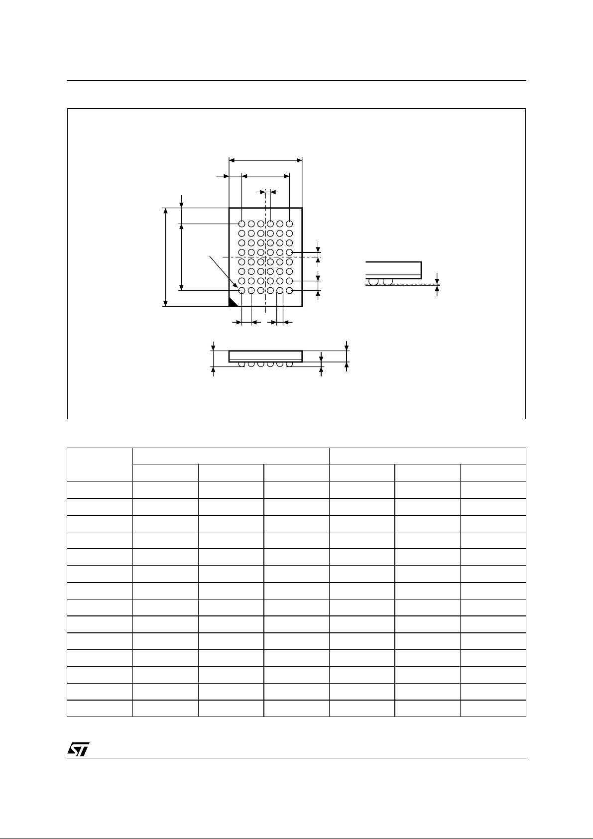
Figure 16.TFBGA48 6x8m m - 6x8 ball array, 0.80 mm pitch, Package Outline . . . . . . . . . . . . . . . 27
Table 17. TFBGA48 6x 8m m - 6x8 ball array, 0.80 mm pitch, Package Mechanical Dat a. . . . . . . . 27
PART NUMBERING . . . . . . . . . . . . . . . . . . . . . . . . . . . . . . . . . . . . . . . . . . . . . . . . . . . . . . . . . . . . . . . 28
Table 18.Ordering Information Scheme . . . . . . . . . . . . . . . . . . . . . . . . . . . . . . . . . . . . . . . . . . . . . 28
3/40
Page 4

M29W160ET, M29W160EB
APPENDIX A.BLOCK ADDRESS TABLE . . . . . . . . . . . . . . . . . . . . . . . . . . . . . . . . . . . . . . . . . . . . . . 29
Table 19. Top Boot Block Addresses, M29W160ET. . . . . . . . . . . . . . . . . . . . . . . . . . . . . . . . . . . . 29
Table 20. Bottom Boot Block Addresses, M29W160EB . . . . . . . . . . . . . . . . . . . . . . . . . . . . . . . . . 29
APPENDIX B.COMMON FLASH INTERFACE (CFI) . . . . . . . . . . . . . . . . . . . . . . . . . . . . . . . . . . . . . . 30
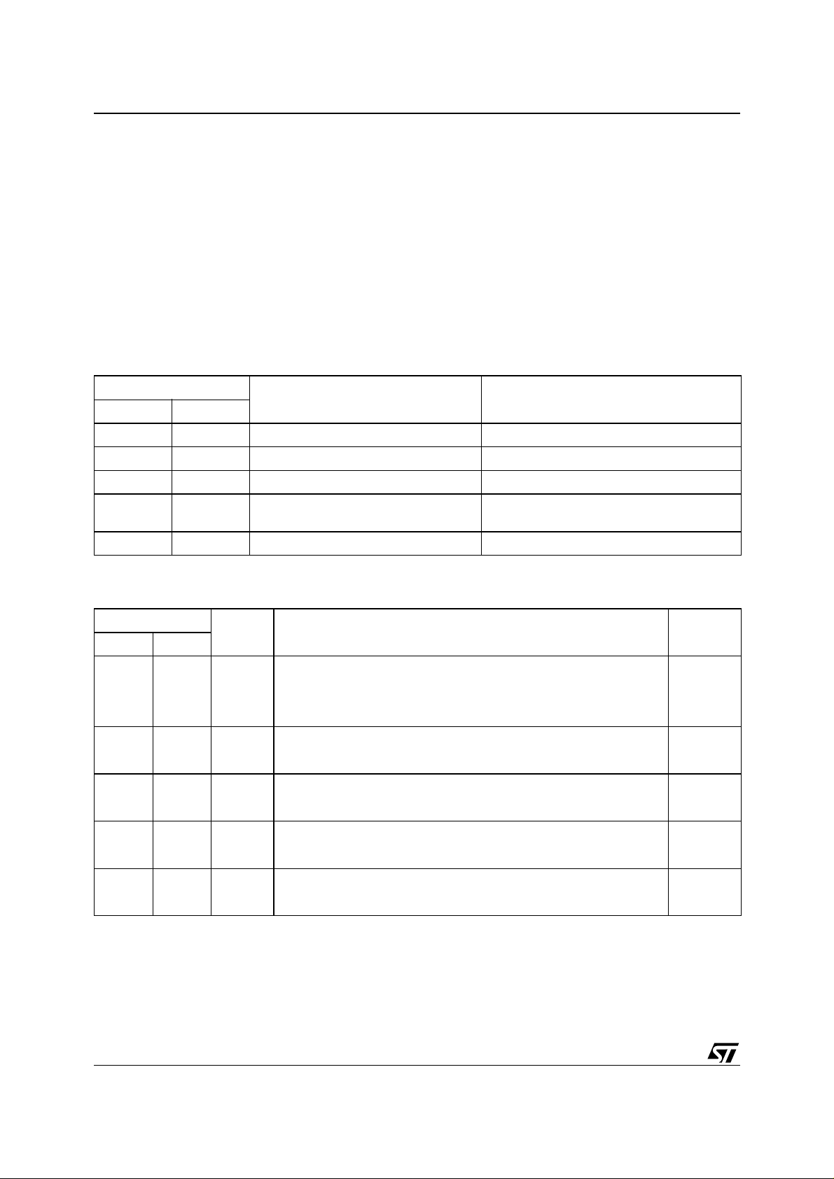
Table 21.Query Structure Overview. . . . . . . . . . . . . . . . . . . . . . . . . . . . . . . . . . . . . . . . . . . . . . . .30
Table 22.CFI Query Identification String. . . . . . . . . . . . . . . . . . . . . . . . . . . . . . . . . . . . . . . . . . . . .30
Table 23. CFI Query System Interface Information. . . . . . . . . . . . . . . . . . . . . . . . . . . . . . . . . . . . . 31
Table 24. Device Geometry Definition . . . . . . . . . . . . . . . . . . . . . . . . . . . . . . . . . . . . . . . . . . . . . .32
Table 25. Primary Algorithm-Specific Extended Query Tabl e . . . . . . . . . . . . . . . . . . . . . . . . . . . . . 33
Table 26.Security Code Area . . . . . . . . . . . . . . . . . . . . . . . . . . . . . . . . . . . . . . . . . . . . . . . . . . . . . 33
APPENDIX C.BLOCK PROTECTION. . . . . . . . . . . . . . . . . . . . . . . . . . . . . . . . . . . . . . . . . . . . . . . . . . 34
Programmer Technique . . . . . . . . . . . . . . . . . . . . . . . . . . . . . . . . . . . . . . . . . . . . . . . . . . . . . . . . 34
In-System Technique . . . . . . . . . . . . . . . . . . . . . . . . . . . . . . . . . . . . . . . . . . . . . . . . . . . . . . . . . . 34
Table 27. Programmer Technique Bus Operations, BYTE
Figure 17.Programmer Equipment Block Protect Flowchart. . . . . . . . . . . . . . . . . . . . . . . . . . . . . . 35
Figure 18.Programmer Equipment Chip Unprotect Flowchart. . . . . . . . . . . . . . . . . . . . . . . . . . . . . 36
Figure 19.In-System Equipment Block Protect Flowchart. . . . . . . . . . . . . . . . . . . . . . . . . . . . . . . .37
Figure 20.In-System Equipment Chip Unprotect Flowchart . . . . . . . . . . . . . . . . . . . . . . . . . . . . . .38
= VIH or V
IL . . . . . . . . . . . . . . . . . . . . . . . . . . . 34
REVISION HISTORY. . . . . . . . . . . . . . . . . . . . . . . . . . . . . . . . . . . . . . . . . . . . . . . . . . . . . . . . . . . . . . . 39
Table 28. Document Revision History. . . . . . . . . . . . . . . . . . . . . . . . . . . . . . . . . . . . . . . . . . . . . . . 39
4/40
Page 5

M29W160ET, M29W160EB
SUMMARY DESCRIPTION
The M29W160E is a 16 Mbit (2Mb x8 or 1Mb x16)
non-volatile memory that can be read, erased and
reprogrammed. These operations can be performed using a single low voltage (2.7 to 3.6V)
supply. On power-up the memory d efaults to its
Read mode where it can be read in the same way
as a ROM or EPROM.
The memory is divided into blocks that can be
erased independently so it is possible to pres erve
valid data while old data is erased. Each block can
be protected independently to prevent accidental
Program or Erase commands from modifying the
memory. Program and Erase c omm ands are wri tten to the Command Interface of t he memory. An
on-chip Program/Erase Controller simplifies the
process of programming or erasing the memory by
taking care of all of the special operations that are
required to update the memory contents.
The end of a program or erase operation can be
detected and any error conditions identified. The
Figure 2. Logic Diagram Table 1. Signal Names
command set required to control the memory is
consistent with JEDEC standards.
The blocks in the memory are asymmetrically arranged, see Figures 5 and 6, Block Addresses.
The first or last 64 KBytes have been divided into
four additional blocks. The 16 KByte Boot Block
can be used for small initialization code to start the
microprocessor, the two 8 KByte Parameter
Blocks can be used for parameter storage and the
remaining 32K is a small Main Block where the application may be stored.
Chip Enable, Output Enable and Write Enable signals control the bus operation of the memory.
They allow simple conne ction to most microprocessors, often without additional logic.
The memory is offered TSOP48 (12 x 20mm) and
TFBGA48 (0.8mm pitch) packages. The memory
is supplied with all the bits erased (set to ’1’).
A0-A19
W
RP
BYTE
A0-A19 Address Inputs
V
CC
20
E
G
M29W160ET
M29W160EB
V
SS
15
DQ0-DQ14
DQ15A–1
RB
AI06849B
DQ0-DQ7 Data Inputs/Outputs
DQ8-DQ14 Data Inputs/Outputs
DQ15A–1 Data Input/Output or Address Input
E
G
W
RP
RB
BYTE
V
CC
V
SS
NC Not Connected Internally
Chip Enable
Output Enable
Write Enable
Reset/Block Temporary Unprotect
Ready/Busy Output
Byte/Word Organization Select
Supply Voltage
Ground
5/40
Page 6

M29W160ET, M29W160EB
Figure 3. TSOP Connection s
A15
A14
A13
A12
A11
1
48
A16
BYTE
V
SS
DQ15A–1
DQ7
A10 DQ14
A9
A8
A19
NC
W
RP
NC
NC
RB
A18
A17
A7
A6
A5
A4
A3
A2
A1
12
M29W160ET
M29W160EB
13
24 25
AI06850
37
36
DQ6
DQ13
DQ5
DQ12
DQ4
V
CC
DQ11
DQ3
DQ10
DQ2
DQ9
DQ1
DQ8
DQ0
G
V
SS
E
A0
6/40
Page 7

Figure 4. TFBGA Connections (Top view through package)
M29W160ET, M29W160EB
654321
A
B
C
D
E
F
G
H
A3
A4
A2
A1
A0
E
G
V
SS
A7
A17
A6
A5 NC
DQ0
DQ8
DQ9
DQ1
RB
NC
A18
DQ2
DQ10
DQ11
DQ3
W
RP
NC
A19
DQ5
DQ12
V
CC
DQ4
A9
A8
A10
A11
DQ7
DQ14
DQ13
DQ6
A13
A12
A14
A15
A16
BYTE
DQ15
A–1
V
SS
AI02985B
7/40
Page 8

M29W160ET, M29W160EB
Figure 5. Block Addresses (x8)
M29W160ET
Top Boot Block Addresses (x8)
1FFFFFh
1FC000h
1FBFFFh
1FA000h
1F9FFFh
1F8000h
1F7FFFh
1F0000h
1EFFFFh
1E0000h
01FFFFh
010000h
00FFFFh
000000h
16 KByte
8 KByte
8 KByte
32 KByte
64 KByte
64 KByte
64 KByte
Total of 31
64 KByte Blocks
Bottom Boot Block Addresses (x8)
1FFFFFh
1F0000h
1EFFFFh
1E0000h
01FFFFh
010000h
00FFFFh
008000h
007FFFh
006000h
005FFFh
004000h
003FFFh
000000h
M29W160EB
64 KByte
64 KByte
64 KByte
32 KByte
8 KByte
8 KByte
16 KByte
Total of 31
64 KByte Blocks
Note: Also see Appendi x A, Tables 19 and 20 for a full l is t i ng of the Block A ddresses .
AI06851
8/40
Page 9

Figure 6. Block Addresses (x16)
M29W160ET, M29W160EB
Top Boot Block Addresses (x16)
FFFFFh
FE000h
FDFFFh
FD000h
FCFFFh
FC000h
FBFFFh
F8000h
F7FFFh
F0000h
0FFFFh
08000h
07FFFh
00000h
M29W160ET
8 KWord
4 KWord
4 KWord
16 KWord
32 KWord
32 KWord
32 KWord
Total of 31
32 KWord Blocks
Bottom Boot Block Addresses (x16)
FFFFFh
F8000h
F7FFFh
F0000h
0FFFFh
08000h
07FFFh
04000h
03FFFh
03000h
02FFFh
02000h
01FFFh
00000h
M29W160EB
32 KWord
32 KWord
32 KWord
16 KWord
4 KWord
4 KWord
8 KWord
Total of 31
32 KWord Blocks
Note: Also see Appendi x A, Tables 19 and 20 for a full l is t i ng of the Block A ddresses .
AI06852
9/40
Page 10

M29W160ET, M29W160EB
SIGNAL DESCRIPTIONS
See Figure 2, Logic Diagram, and Table 1, Sign al
Names, for a brief overview of the signals connected to this de vice.
Address Inputs (A0-A19). The Address Inputs
select the cell s in the memory arra y to access du ring Bus Read operations. During Bus Write operations they control the commands sent to the
Command Interface of the Program/Erase Controller.
Data Inputs/Outputs (DQ0-DQ7). The Data Inputs/Outputs output the data stored at the selected
address during a Bus Read operation. During Bus
Write operations they represent the commands
sent to the Command Interface of the Program/
Erase Controller.
Data Inputs/Outputs (DQ8-DQ14). The Data Inputs/Outputs output the data stored at the selected
address during a Bus Read operation when BYTE
is High, VIH. When BYTE is Low, VIL, these pins
are not used and are high impedance. During Bus
Write operations the Command Register does not
use these bits. When reading the S tatus Register
these bits should be ignored.
Data Input/Ou tput or Address Input (DQ15A-1).
When BYTE
Data Input/Output pin (as DQ8-DQ14). When
BYTE
pin; DQ15A–1 Low will select the LSB of the Word
on the other addresses, DQ15A–1 High will select
the MSB. Throughout the text consider references
to the Data Input/Output to include this pin when
BYTE
puts to include this pin when BYTE
when stated explicitly otherwise.
Chip Enable (E
the memory, allowing Bus Read and Bus Write operations to be performed. When Chip Enable is
High, V
Output Enable (G
trols the Bus Read operation of the memory.
Write Enable (W
the Bus Write operation of the memory’s Command Interf a ce .
Reset/Block Temporary Unprotect (RP
Reset/Block Temporary Unprotect pin can be
used to apply a Hardware Reset to the memory or
to temporarily unprotect all Blocks that have b een
protected.
A Hardware Reset is achieved by holding Reset/
Block Temporary Unprotect Low, V
. After Reset/Block Temporary Unprotect
t
PLPX
goes High, V
is High, VIH, this pin behaves as a
is Low, VIL, this pin behaves as an address
is High and ref erences to the Address In-
is Low except
). The Chip Enable, E, activates
, all other pins are ignored.
IH
). T he Output Enable, G, con-
). The Write Enable, W, controls
). The
, for at least
IL
, the memory will be ready for Bus
IH
Read and Bus Write operations after t
, whichever occurs last. See the Ready/Busy
t
RHEL
PHEL
or
Output section, Table 15 and Figure 14, Reset/
Temporary Unprotect AC Characteristics for more
details.
Holding RP
at VID will temporarily unprotect the
protected Blocks in the memory. Program and
Erase operations on all blocks will be possible.
The transition from V
PHPHH
.
t
Ready/Busy Output (RB
to VID must be slower than
IH
). The Ready/Busy pin
is an open-drain output that can be used to identify
when the device is performing a Program or Erase
operation. During Program or Erase operations
Ready/Busy is Low, V
. Ready/Busy is high-im-
OL
pedance during Read mode, Auto Select mode
and Erase Suspend mode.
After a Hardware Reset, Bus Read and Bus Write
operations cannot begin until Ready/Busy becomes high-impedance. See Tabl e 15 and Figure
14, Reset/Temporary Unprotect AC Characteristics.
The use of an open-drain output allows the Ready/
Busy pins from several memories to be connected
to a single pull-up resistor. A Low will then indicate
that one, or more, of the memories is busy.
Byte/Word Organization Select (BYTE
). The
Byte/Word Organization Select pin is used to
switch between the 8-bit and 16-bit Bus modes of
the memory. When Byte/Word Organization Select is Low, V
it is High, V
Supply Voltage. The VCC Supply Voltage
V
CC
, the memory is in 8-bit mode, when
IL
, the memory is in 16-bit mode.
IH
supplies the power for all operations (Read, Program, Erase etc.).
The Command Interface is disabled when the V
CC
Supply Voltage is less than the L ockout Voltage,
. This prevents Bus Write operations from ac-
V
LKO
cidentally damaging the data during power up,
power down and power surges. If the Program/
Erase Controller is programming or erasing during
this time then the operation aborts and the memory contents being altered will be invalid.
A 0.1µF capacitor should be connected between
the V
Supply Voltage pin and the VSS Ground
CC
pin to decouple the current surges from the power
supply. The PCB track widths must be sufficient to
carry the currents required during program and
erase operations, I
Ground. The VSS Ground is the reference for
V
SS
all voltage measurements. The two V
CC3
.
pins of the
SS
device must be connected to the system ground.
10/40
Page 11

BUS OPERATIONS
There are five standard bus operations that control
the device. These are Bus Read, Bus Write, Ou tput Disable, Standby and Automatic Standby. See
Tables 2 and 3, Bus Operat ions, for a summary.
Typically glitches of less than 5ns on Chip Enable
or Write Enable are ignored by the memory and do
not affect bus operations.
Bus Read. Bus Read operations read from the
memory cells, or specific registers in the Command Interface. A valid Bus Read operation involves setting the desired address on the Address
Inputs, applying a Low sig nal, V
, to Chip Enable
IL
and Output Enable and keeping Write Enable
High, V
. The Data Inputs/Outputs will output the
IH
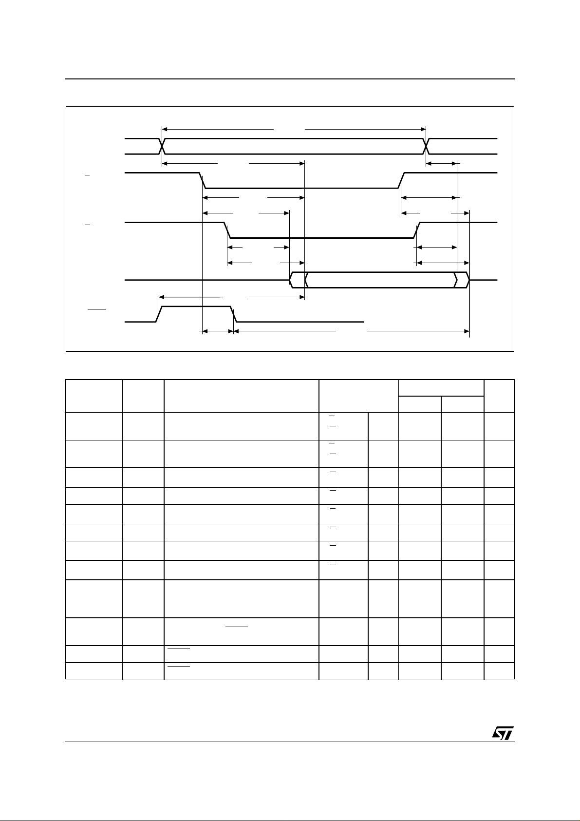
value, see Figure 11, Read Mode AC Waveforms,
and Table 12, Read AC Characteristics, for details
of when the output becomes valid.
Bus Write. Bus Write operations write to the
Command Interface. A valid Bus Write operation
begins by setting the desire d address on t he Address Inputs. The Address Inputs are latc hed by
the Command Interface on the falling edge of Chip
Enable or Write Enable, whichever occurs last.
The Data Inputs/Outputs a re latched by the Command Interface on the rising edge of Chip Enable
or Write Enable, whichever occurs first. Output Enable must remain High, V
, during the whole Bus
IH
Write operation. See Figures 12 and 13, Write AC
Waveforms, and Tables 13 and 14, Write AC
Characteristics, for details of the timing requirements.
Output Disa bl e . The Data Inputs/Outputs are in
the high impedance s tate when Output Enable is
High, V
Standby. When Chip Enable is High, V
.
IH
, the
IH
memory enters Standby mode and the Data Inputs/Outputs pins are placed in the high-imped-
M29W160ET, M29W160EB
ance state. To reduce t he Supply Current to the
Standby Supply Current, I
be held within V
± 0.2V. For the Standby current
CC
level see Table 11, DC Characteristics.
During program or erase operations the memory
will continue to use the Program/Erase Supply
Current, I
, for Program or Erase operations un-
CC3
til the operation completes.
Automatic Standby. If CMOS levels (V
are used to drive the bus and the bus is inactive for
150ns or more the memory enters Automatic
Standby where the internal Supply Current is reduced to the Standby Supply Current, I
Data Inputs/Outputs will still output data if a Bus
Read operation is in progress.
Special Bus Operations. Additional bus operations can be performed to read the Electronic Signature and also to apply and remove Block
Protection. These bus operations are intended for
use by programming equipment and are not usually used in applications. They require V
applied to some pins.
Electronic Signature. The memory has two
codes, the manufacturer code and the device
code, that can be read to identify the memory.
These codes can be read by applying t he signals
listed in Tables 2 and 3, Bus Operations.
Block Protection and Blocks Unprotection.
Each block can be separately protected against
accidental Program or Erase. Protected blocks
can be unprotected to allow data to be changed.
There are two methods available for protecting
and unprotecting the blocks, one for use on programming equipment and the other for in-system
use. Block Protect and Blocks Unprotect operations are described in Appendix C.
, Chip Enable should
CC2
CC
CC2
± 0.2V)
. The
to be
ID
Table 2. Bus Operations, BYTE
Operation E G W
Bus Read
Bus Write
Output Disable X
Standby
Read Manufacturer
Code
Read Device Code
Note: X = VIL or VIH.
V
IL
V
IL
V
IH
V
IL
V
IL
= V
IL
Address Inputs
DQ15A–1, A0-A19
V
IL
V
IH
V
IH
X X X Hi-Z Hi-Z
V
IL
V
IL
V
Cell Address Hi-Z Data Output
IH
V
Command Address Hi-Z Data Input
IL
V
X Hi-Z Hi-Z
IH
A0 = VIL, A1 = VIL, A9 = VID,
V
IH
Others V
A0 = VIH, A1 = VIL, A9 = VID,
V
IH
Others V
IL
IL
or V
or V
IH
IH
Data Inputs/Outputs
DQ14-DQ8 DQ7-DQ0
Hi-Z 20h
Hi-Z
C4h (M29W160ET)
49h (M29W160EB)
11/40
Page 12

M29W160ET, M29W160EB
Table 3. Bus Operations, BYTE = V
Operation E G W
Bus Read
Bus Write
Output Disable X
Standby
Read Manufacturer
Code
Read Device Code
Note: X = VIL or VIH.
V
IL
V
IL
V
IH
V
IL
V
IL
IH
V
IL
V
IH
V
IH
XXX Hi-Z
V
IL
V
IL
V
Cell Address Data Output
IH
V
Command Address Data Input
IL
V
XHi-Z
IH
A0 = VIL, A1 = VIL, A9 = VID,
V
IH
Others V
A0 = VIH, A1 = VIL, A9 = VID,
V
IH
Others V
COMMAND INTERFACE
All Bus Write operations t o the me mory are in terpreted by the Command Interface. Commands
consist of one or more sequential Bus Write operations. Failure to observe a valid sequence of Bus
Write operations will result in the memory returning to Read mode. The long command sequences
are imposed to maximize data security.
The address used for the commands changes depending on whether the memory is in 16-bit or 8bit mode. See either Table 4, or 5, de pending on
the configuration that is being used, for a summary
of the commands.
Read/Reset Command. The Read/Reset command returns the memory to its Read mode where
it behaves like a ROM or EPROM, unless otherwise stated. It also resets the errors in th e Status
Register. Either one or three Bus Write operations
can be used to issue the Read/Reset command.
The Read/Reset Command can be issued, between Bus Write cycles before the start of a program or erase operation, to return the device to
read mode. Once the program or erase operation
has started the Read/Reset command is no longer
accepted. The Read/Reset command will not
abort an Erase operation when issued while in
Erase Suspend.
Auto Select Command. The Auto Select command is used to read the Manufacturer Code, the
Device Code and the Block Protection Status.
Three consecutive Bus Write operations are required to issue the Auto Select command. Once
the Auto Select comma nd is issued the memory
remains in Auto Select mode until a Read/Reset
command is issued. Read CFI Query and Read/
Reset commands are accepted in Auto Select
mode, all other commands are ignored.
Address Inputs
A0-A19
or V
IL
IH
or V
IL
IH
Data Inputs/Outputs
DQ15A–1, DQ14-DQ0
0020h
22C4h (M29W160ET)
2249h (M29W160EB)
From the Auto Select mode the Manufacturer
Code can be read using a Bus Read operation
with A0 = V
may be set to either V
and A1 = VIL. The other address bits
IL
or VIH. The Manufa cturer
IL
Code for STMicroelectronics is 0020h.
The Device Code can be read using a Bus Read
operation with A0 = V
address bits may be set to e ither V
and A1 = VIL. The other
IH
or VIH. The
IL
Device Code for the M29W160ET is 22C4h and
for the M29W160EB is 2249h.
The B lock Prot ection S tatus of each block can be
read using a Bus Read operation with A0 = V
A1 = V
, and A 12 - A19 spec ify i ng the ad dress of
IH
the bl ock. T he oth er addr ess bit s may b e set t o either V
or VIH. If the ad dress ed bloc k is pro tecte d
IL
then 01h is output on Data Inputs/Outputs DQ0DQ7, otherwise 00h is output.
Program Command. The Program command
can be used to program a value to one address in
the memory array at a time. The command requires four Bus Write operations, the final write operation latches the address and data, and starts
the Program/Erase Controller.
If the address falls in a pro tected block then the
Program command is ignored, the data remains
unchanged. The Status Register is never read and
no error condition is given.
During the program operat ion the memo ry will ignore all commands. I t is not possible to issue any
command to abort or pause the operation. Typical
program times are given in Table 6. Bus Read operations during the program o peration will output
the Status Register on the Data Inputs/Outputs.
See the section on the S tatus Register for more
details.
After the program operation has completed the
memory returns to the Read mode, unless an error
,
IL
12/40
Page 13

M29W160ET, M29W160EB
has occurred. When an error occurs the me mory
continues to output the St atus Register. A Read/
Reset command must be issued to reset the error
condition and return to Read mode.
Note that the Program command cannot change a
bit set at ’0’ bac k to ’1’. One of the E rase Commands must be used to set all the bits in a block or
in the whole memory from ’0’ to ’1’.
Unlock Bypass Command. The Unlock Bypass
command is used in conjunction with the Unlock
Bypass Program command to program the memory. When the access time to the device is long (as
with some EPROM programmers) considerable
time saving can be made by using these commands. Three Bus Write operations are requ ired
to issue the Unlock Bypass command.
Once the Unlock Bypas s command has bee n issued the memory will only accept the Unl ock Bypass Program command and the Unlock Bypass
Reset command. The memory can be read as if in
Read mode.
Unlock Bypass Program Command. The Unlock Bypass Prog ram comma nd can be used to
program one address in memory at a time. The
command requires two Bus Write operations, the
final write operation latches the address and data,
and starts the Program/Erase Controller.
The Program operation using the Unlock Bypass
Program command behaves identically to the Program operation using the Program command. A
protected block cannot be programmed; the operation cannot be aborted and the Status Register is
read. Errors must be res et using the Rea d/Reset
command, which leav es the de vice in Unlo ck Bypass Mode. See the Program command for details
on the behavior.
Unlock Bypass Reset Command. The Unlock
Bypass Reset command can be used to ret urn to
Read/Reset mode from Unlock Bypass Mode.
Two Bus Write operations are required to issue the
Unlock Bypass Reset command. Read/Reset
command does not exit from Unlock Bypass
Mode.
Chip Erase Command. The Chip Erase command can be used to erase the entire chip. Six Bus
Write operations are required to issue the Chip
Erase Command and start the Program/Erase
Controller.
If any blocks are protected then these are ignored
and all the other blocks are erased. If all of the
blocks are protect e d th e Chip Erase op erat i on appears to start but will terminate within about 100µs,
leaving the data unchanged. No error condition is
given when protected blocks are ignored.
During the erase operation the memory will ignore
all commands. It is not possible to issue any command to abort the operation. Typical chip erase
times are given in Tabl e 6. All Bus Read operations during the Chip E rase operation will output
the Status Register on the Data Inputs/Outputs.
See the section on the S tatus Register for more
details.
After the Chip Erase operation has com pleted the
memory will retu rn to the Read Mode, unless an
error has occurred. When an error occurs the
memory will continue to output the Status Register. A Read/Reset command must be issued to reset the error condition and return to Read Mode.
The Chip Erase Command sets all of the bits in unprotected blocks of the memory to ’1’. All previous
data is lost.
Block Erase Command. The Block Erase command can be u sed to erase a list of one or more
blocks. Six Bus Write operations are required to
select the first block in the list. Each additional
block in the list can be selected by repeating the
sixth Bus Write operation using the address of the
additional block. The Block Erase operation starts
the Program/Erase Controller about 50µs after the
last Bus Write operation. Once the Program/Erase
Controller starts it is not possible to select any
more blocks. Each additional block must therefore
be selected within 50µs of the last block. The 50µs
timer restarts when an additional block is selected.
The Status Register can be read after the sixth
Bus Write operation. See the Status Register section for details on how t o identify if the Program/
Erase Controller has started the Block Erase operation.
If any selected blocks are protected then these are
ignored and all the other selected blocks are
erased. If all of the selected blocks are pro tected
the Block Erase operation appears to start but will
terminate within about 100µs, leaving the data unchanged. No error condition is given when protected blocks are ignored.
During the Block Erase operation the me mory wi ll
ignore all commands except the Erase Susp end
command. Typical b lock e rase times a re g iven in
Table 6. All Bus Read operations during the Block
Erase ope ration will ou t p ut the S t a tus R eg i st er on
the Data Inputs/Outputs. See the sec tion on the
Status Register for more details.
After the Block Erase operation has completed the
memory will retu rn to the Read Mode, unless an
error has occurred. When an error occurs the
memory will continue to output the Status Register. A Read/Reset command must be issued to reset the error condition and return to Read mode.
The Block Erase Command sets all of the bits in
the unprotected selected blocks to ’1’. All previous
data in the selected blocks is lost.
Erase Suspend Command. The Erase Suspend
Command may be used to temporarily suspend a
13/40
Page 14

M29W160ET, M29W160EB
Block Erase operation and return the memory to
Read mode. The command requires one Bus
Write operation.
The Program/Erase Controller will sus pend within
the Erase Suspend Latency Time (refer to Table 6
for value) of the Erase Suspend Command being
issued. Once the Program/Erase Controller has
stopped the memory will be set to Read mode and
the Erase will be suspended. If the Erase Suspend
command is issued during the period when the
memory is waiting for an additional block (before
the Program/Erase Controller starts) then the
Erase is suspended immedi ately and wi ll start immediately when the Erase Resume Comm and is
issued. It is not possible to select any further
blocks to erase after the Era se Resume.
During Erase Suspend it is possible to Read and
Program cells in blocks that are not being erased;
both Read and Program operations behave as
normal on these blocks. If any attempt is made to
program in a protected block or in the suspended
block then the Program command is ignored and
the data remains unchanged. The Status Register
is not read and no error condi tion is given. Reading from blocks that are being erased will output
the Status Register.
It is also possible t o issue the Auto Select, Read
CFI Query and Unlock Bypass commands during
an Erase Suspend. The Read/Reset command
must be issued to return the device to Read Array
mode before the Resume command will be accepted.
Erase Resume Command. The Erase Resume
command must be used to restart the Program/
Erase Controller from Erase Susp end. An erase
can be suspended and resumed more than once.
Read CFI Query Command. The Read CFI
Query Command is used to read data from the
Common Flash Interface (CFI) Memory Area. This
command is valid when the device is in the Read
Array mode, or when the device is in Aut o Sel ect
mode.
One Bus Write cycle is required to issue the Read
CFI Query Command. Once the command is issued subsequent Bus Read ope rations read from
the Common Flash Interface Memory Area.
The Read/Reset command m ust be issued to return the device to the previous mode (the Read Array mode or Auto Select mode). A second Read/
Reset command would be needed if the device is
to be put in the Read Array mode from Auto Select
mode.
See Appendix B, Tables 21, 22, 23, 24, 25 and 26
for details on the information contained in the
Common Flash Interface (CFI) memory area.
14/40
Page 15
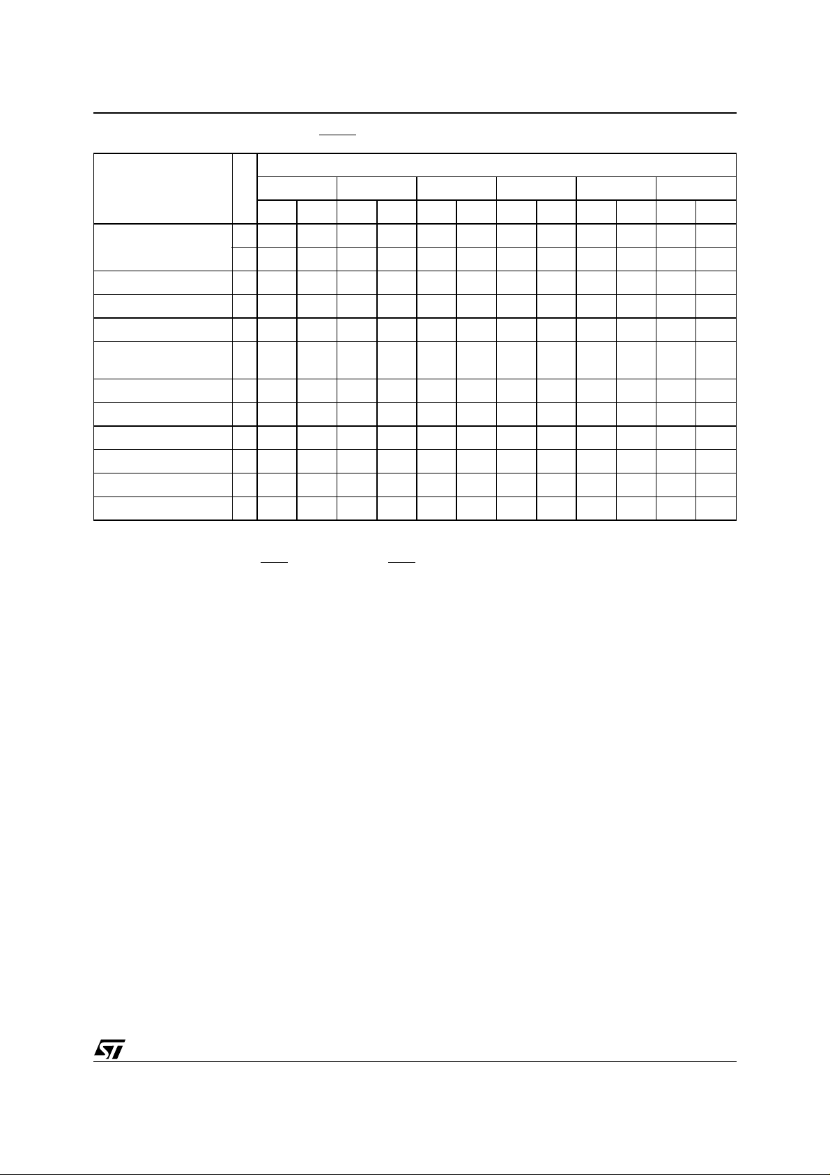
M29W160ET, M29W160EB
Table 4. Commands, 16-bit mode, BYTE = V
IH
Bus Write Operations
Command
1st 2nd 3rd 4th 5th 6th
Length
Addr Data Addr Data Addr Data Addr Data Addr Data Addr Data
1X F0
Read/Reset
3555 AA2AA 55 X F0
Auto Select 3 555 AA 2AA 55 555 90
Program 4 555 AA 2AA 55 555 A0 PA PD
Unlock Bypass 3 555 AA 2AA 55 555 20
Unlock Bypass
Program
2X A0PAPD
Unlock Bypass Reset 2 X 90 X 00
Chip Erase 6 555 AA 2AA 55 555 80 555 AA 2AA 55 555 10
Block Erase 6+ 555 AA 2AA 55 555 80 555 AA 2AA 55 BA 30
Erase Suspend 1 X B0
Erase Resume 1 X 30
Read CFI Query 1 55 98
Note: X Don’t Care, PA Program Address, PD Program Data, BA Any address in the Block.
All values in the table are in hexadecim al .
The Comm and In terf ace o nly uses A– 1, A 0-A1 0 a nd DQ0-D Q7 to v er ify t he co mm ands ; A1 1-A1 9, D Q8- DQ1 4 and DQ 15 are D on’t
Care. DQ15A–1 is A– 1 when BYTE
Read/Reset. After a Read/Re set command, read the mem ory as normal until another command is issued.
Auto Select. After an Auto Sel ect command, read Manu facturer ID , Device ID or Block Protection Status.
Program, Unlo ck Byp ass Prog ra m, Ch ip Eras e, Block E ras e. A fte r thes e comm an ds rea d the S tat us Reg ister unti l the Pr og ram/
Erase Controller completes and the memory returns to Read Mode. Add additional Blocks during Block Erase Command with additional
Bus Write Operations until Timeou t Bit is set.
Unloc k By p as s. After th e Unlock Byp ass comman d i ssue Unlock Bypass Program or Unlock Bypass Reset comm ands.
Unloc k By p as s Reset. After the Unlock Bypass Reset command read the memory as normal until another command is issued.
Erase Suspend. After the Erase Suspend command read non-erasing memory blocks as normal, issue Auto Select and Program com-
mands on no n-erasin g bl oc ks as normal.
Erase Resume. A f ter the Erase Resume command the su spended Er ase operat i on resume s, read the S t atus Register unti l the Pro-
gram/ Erase Controll e r c o m pl e t e s an d t h e m em ory ret ur ns to Read Mode.
CFI Query. Command is valid when device is ready to rea d array data or when device i s i n A uto Select mode.
is VIL or DQ15 when BYTE is VIH.
15/40
Page 16
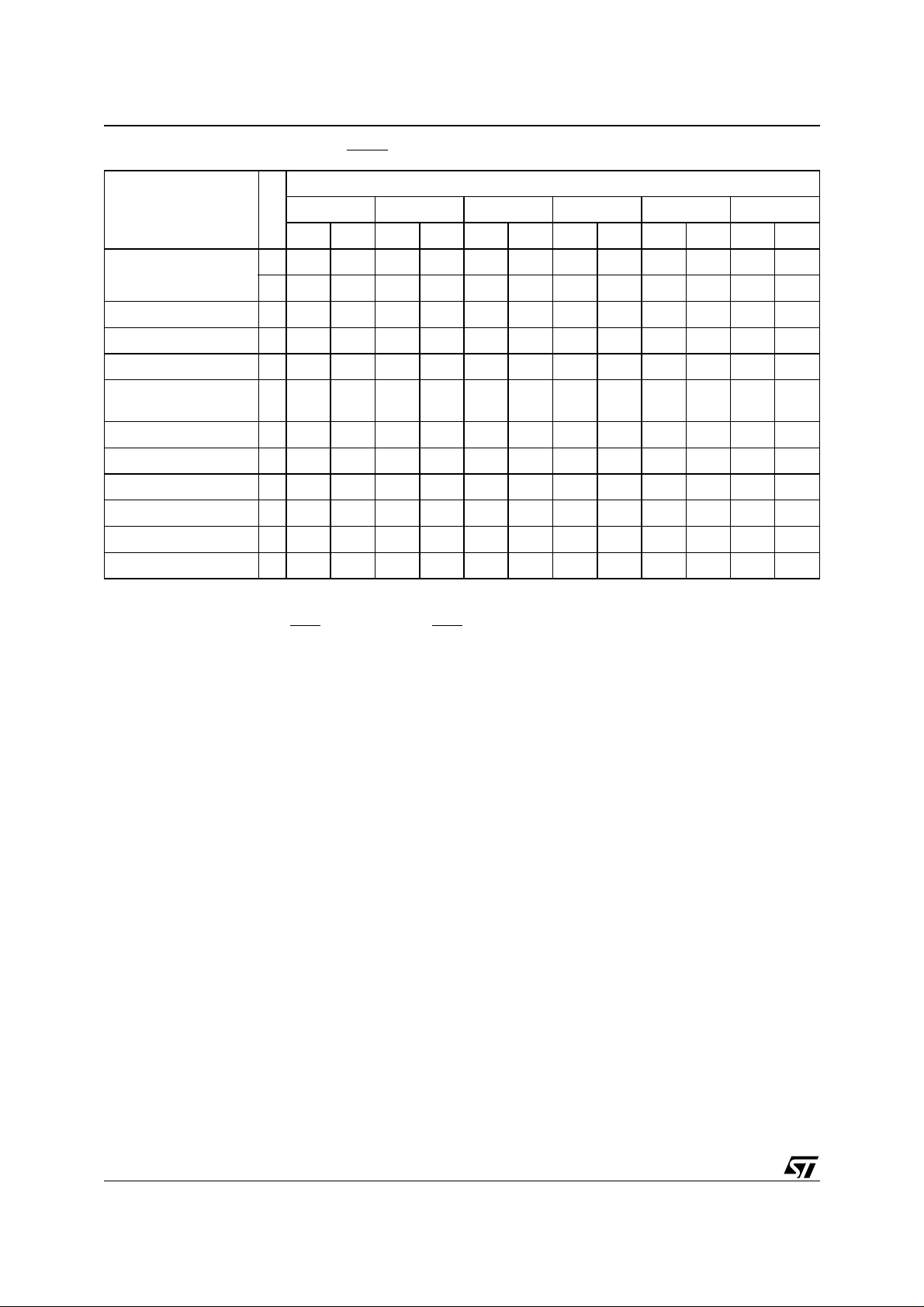
M29W160ET, M29W160EB
Table 5. Commands, 8-bit mode, BYTE = V
IL
Bus Write Operations
Command
1st 2nd 3rd 4th 5th 6th
Length
Addr Data Addr Data Addr Data Addr Data Addr Data Addr Data
1X F0
Read/Reset
3 AAA AA 555 55 X F0
Auto Select 3 AAA AA 555 55 AAA 90
Program 4 AAA AA 555 55 AAA A0 PA PD
Unlock Bypass 3 AAA AA 555 55 AAA 20
Unlock Bypass
Program
2X A0PAPD
Unlock Bypass Reset 2 X 90 X 00
Chip Erase 6 AAA AA 555 55 AAA 80 AAA AA 555 55 AAA 10
Block Erase 6+ AAA AA 555 55 AAA 80 AAA AA 555 55 BA 30
Erase Suspend 1 X B0
Erase Resume 1 X 30
Read CFI Query 1 AA 98
Note: X Don’t Care, PA Program Address, PD Program Data, BA Any address in the Block.
All values in the table are in hexadecim al .
The Comm and In terf ace o nly uses A– 1, A 0-A1 0 a nd DQ0-D Q7 to v er ify t he co mm ands ; A1 1-A1 9, D Q8- DQ1 4 and DQ 15 are D on’t
Care. DQ15A–1 is A– 1 when BYTE
Read/Reset. After a Read/Re set command, read the mem ory as normal until another command is issued.
Auto Select. After an Auto Sel ect command, read Manu facturer ID , Device ID or Block Protection Status.
Program, Unlo ck Byp ass Prog ra m, Ch ip Eras e, Block E ras e. A fte r thes e comm an ds rea d the S tat us Reg ister unti l the Pr og ram/
Erase Controller completes and the memory returns to Read Mode. Add additional Blocks during Block Erase Command with additional
Bus Write Operations until Timeou t Bit is set.
Unloc k By p as s. After th e Unlock Byp ass comman d i ssue Unlock Bypass Program or Unlock Bypass Reset comm ands.
Unloc k By p as s Reset. After the Unlock Bypass Reset command read the memory as normal until another command is issued.
Erase Suspend. After the Erase Suspend command read non-erasing memory blocks as normal, issue Auto Select and Program com-
mands on no n-erasin g bl oc ks as normal.
Erase Resume. A f ter the Erase Resume command the su spended Er ase operat i on resume s, read the S t atus Register unti l the Pro-
gram/ Erase Controll e r c o m pl e t e s an d t h e m em ory ret ur ns to Read Mode.
CFI Query. Command is valid when device is ready to rea d array data or when device i s i n A uto Select mode.
is VIL or DQ15 when BYTE is VIH.
16/40
Page 17
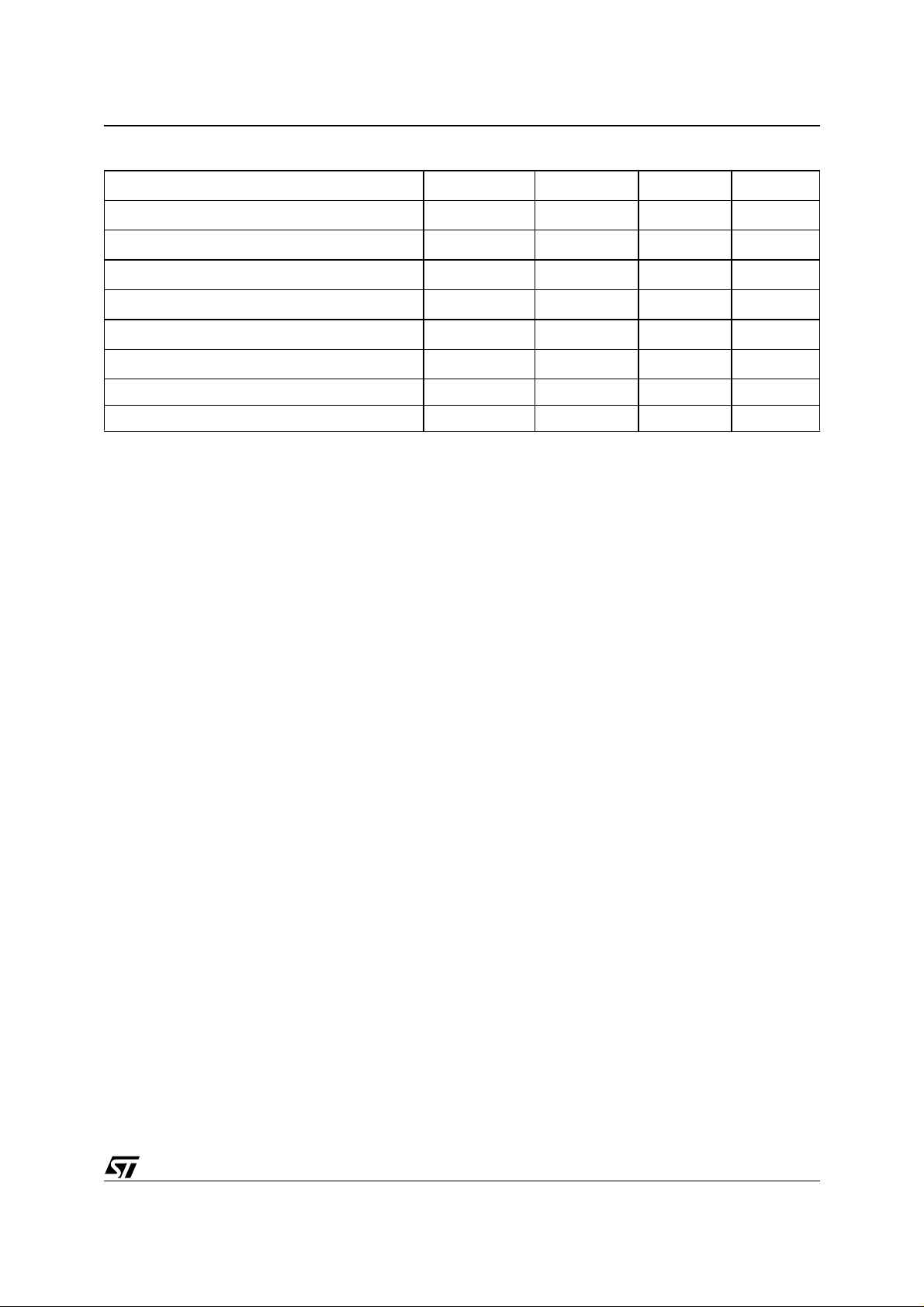
M29W160ET, M29W160EB
Table 6. Program, Erase Times and Progra m , Erase Endu ran ce Cycle s
Parameter Min
Chip Erase 29
Block Erase (64 KBytes) 0.8
Erase Suspend Latency Time 20
Program (Byte or Word) 13
Chip Program (Byte by Byte) 26
Chip Program (Word by Word) 13
Program/Erase Cycles (per Block) 100,000 cycles
Data Retention 20 years
Note: 1. Typical value s m easured at room tempera ture and nom i nal voltages.
2. Sampled, but no t 100% tested.
3. Maximum valu e m easured at worst case conditions for both temperature and V
4. Maximum valu e m easured at worst case conditions for both temperature and V
(1,2)
Typ
after 100,000 program/erase cycles .
CC
.
CC
STATUS REGISTER
Bus Read operations from any address always
read the Status Register during Program and
Erase operations. It is also read during Erase Suspend when an address within a block being erased
is accessed.
The bits in the Status Register are summari zed in
Table 7, Status Register Bits.
Data Polling Bit (DQ7). The Data Polling Bit can
be used to identify whether the Program/Erase
Controller has successfully completed its operation or if it has responded to an Erase Suspend.
The Data Polling Bit is out put on DQ7 when the
Status Register is read.
During Program operations the Data Polling Bit
outputs the complement of the bit being programmed to DQ7. After successful completion of
the Program operation the memory returns to
Read mode and Bus Read operations from the address just programmed o utput DQ7, not its complement.
During Er ase ope ratio ns the D ata Pollin g Bit ou tputs ’0’, the complement of the erased state of
DQ7. After successful completion of the Erase operation the memory returns to Read Mode.
In Erase Suspend mode the Data Polling Bit will
output a ’1’ during a Bus Read operation within a
block being erased. The Data Polling Bit will
change from a ’0’ to a ’1’ when the Program/Erase
Controller has suspended the Erase operation.
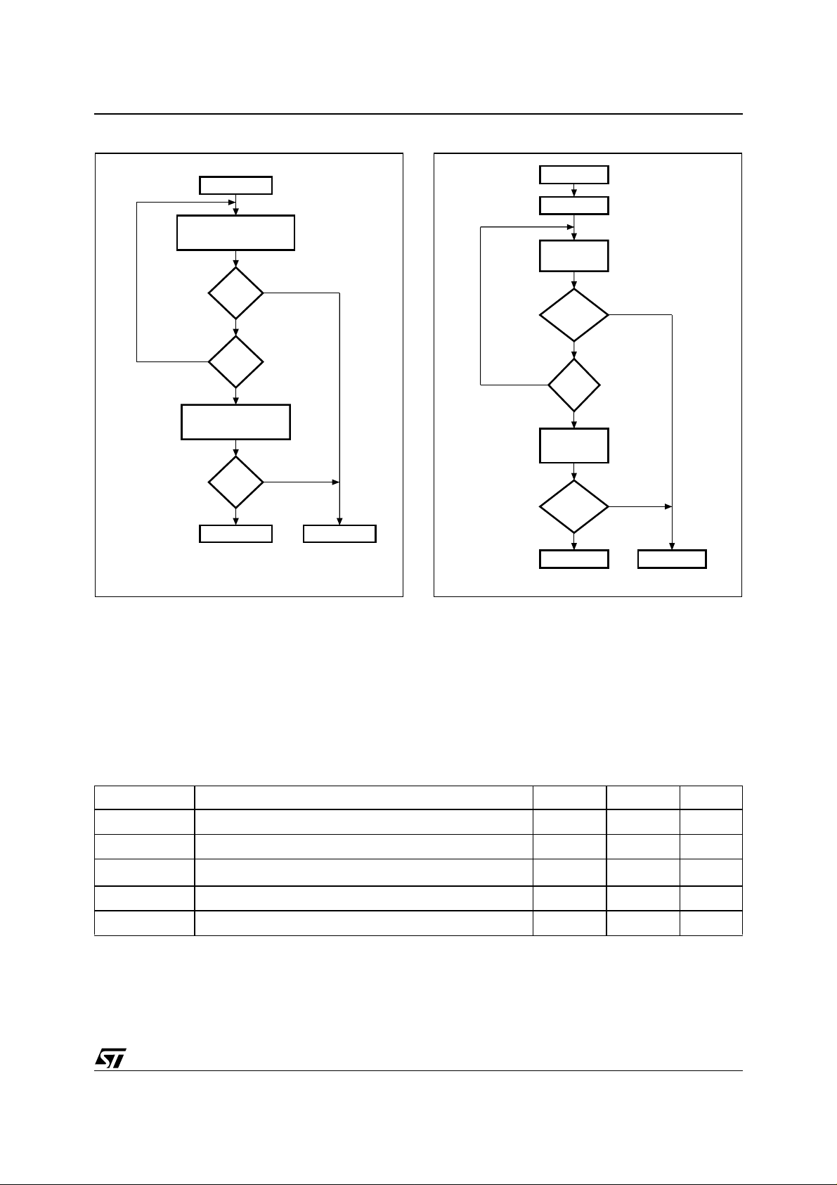
Figure 7, Data Polling Flowchart, gives an e xample of how to use the Data Polling Bit. A Valid Address is the address being programmed or an
Toggle Bit (DQ6). The Toggle Bit can be used to
identify whether the Program/Erase Controller has
successfully completed its operation or if it has responded to an Erase Suspen d. The Toggle Bit is
output on DQ6 when the Status Register is read.
During Program and Erase operations the Toggle
Bit changes from ’0’ to ’ 1’ to ’0’, etc., with successive Bus Read operations at any address. After
successful completion of the operation the memory returns to Read mode.
During Erase Suspend mode the Toggle Bit will
output when addressing a cell within a block being
erased. The Toggle Bit will stop toggling when the
Program/Erase Controller has suspended the
Erase operation.
If any attempt is made to erase a protected bl ock,
the operation is abort ed, no error is s ig nalled and
DQ6 toggles for approximately 100µs. If any attempt is made to program a protected block or a
suspended block, the operation is abort ed, no error is signalled and DQ6 toggles for approximately
1µs.
Figure 8, Data Toggle Flowchart, g ives an e xample of how to use the Data Toggle Bit.
Error Bit (DQ5). The Error Bit can be used to
identify errors detected by the Program/Erase
Controller. The Error Bit i s set to ’1’ when a P rogram, Block Erase or Chip Erase operation fails to
write the correct data to the memory. If the Error
Bit is set a Read/Rese t comm and must be issued
before other commands are issued. The Error bit
is output on DQ5 when the Status Register is read.
address within the block being erased.
Max
120
6
25
200
120
60
(4)
(4)
(3)
(3)
(3)
(3)
(2)
Unit
µs
µs
s
s
s
s
17/40
Page 18
M29W160ET, M29W160EB
Note that the Program command cannot change a
bit set to ’0’ back to ’1’ and attempting to do so will
set DQ5 to ‘1’. A Bus Read operation to that address will s h ow the bit is still ‘ 0 ’. One of the Er as e
commands must b e used to set all the bits in a
block or in the whole memory from ’0’ to ’1’
Erase Timer Bit (DQ3). The Erase Timer Bit can
be used to identify the start of Program/Erase
Controller operation during a Block Erase command. Once the Program/Erase Controller starts
erasing the Erase Timer Bit is set to ’1’. Before the
Program/Erase Controller starts the Erase Timer
Bit is set to ’0’ and additional blocks to be erased
may be written to the Command Interface. The
Erase Timer Bit is output on DQ3 when the Status
Register is read.
Alternative Toggle Bit (DQ2). The Alternative
Toggle Bit can be used to monitor the Program/
Erase controller during Erase operations. The Alternative Toggle Bit is output on DQ2 when the
Status Register is read.
During Chip Erase and Block Erase operations the
Toggle Bit changes from ’0’ to ’1’ to ’0’, etc., with
successive Bus Read operations from addresses
within the blocks being erased. A protected block
is treated the same as a block not being erased.
Once the operation completes the memory returns
to Read mode.
During Erase Suspend the Alternative Toggle Bit
changes from ’0’ to ’1’ to ’0’, etc. with successive
Bus Read operations from addresses within the
blocks being erased. Bus Read operations to addresses within blocks not being erased will ou tput
the memory cell data as if in Read mode.
After an Erase operation that c auses the Error Bit
to be set the Alternative Toggle Bit can be used to
identify which block or blocks have caused the error. The Alternative Toggle Bit changes from ’0’ to
’1’ to ’0’, etc. with successive B us Read Operations from addresses within blocks that have not
erased correctly. The Alternative Toggle B it does
not change if the addressed block has erased correctly.
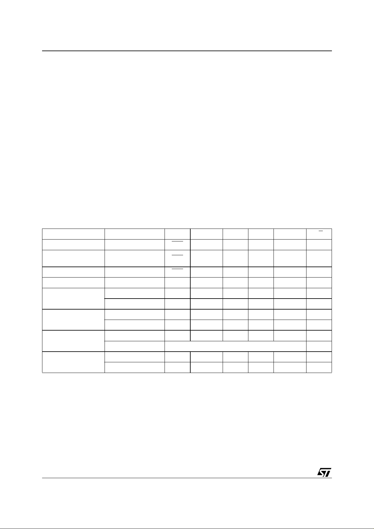
Table 7. Status Register Bits
Operation Address DQ7 DQ6 DQ5 DQ3 DQ2 RB
Program Any Address DQ7 Toggle 0 – – 0
Program During Erase
Suspend
Program Error Any Address DQ7
Chip Erase Any Address 0 Toggle 0 1 Toggle 0
Block Erase before
timeout
Block Erase
Erase Suspend
Erase Er ror
Note: Unspecified data bits should be ignored.
Any Address DQ7
Erasing Block 0 Toggle 0 0 Toggle 0
Non-Erasing Block 0 Toggle 0 0 No Toggle 0
Erasing Block 0 Toggle 0 1 Toggle 0
Non-Erasing Block 0 Toggle 0 1 No Toggle 0
Erasing Block 1 No Toggle 0 – Toggle 1
Non-Erasing Block Data read as normal 1
Good Block Address 0 Toggle 1 1 No Toggle 0
Faulty Block Address 0 Toggle 1 1 Toggle 0
Toggle 0 – – 0
Toggle 1 – – 0
18/40
Page 19
M29W160ET, M29W160EB
Figure 7. Dat a Po ll i ng Fl o w chart Figure 8. Dat a Toggle Flowchart
START
READ DQ5 & DQ7
at VALID ADDRESS
DQ7
DATA
NO
DQ5
READ DQ7
at VALID ADDRESS
DQ7
DATA
FAIL PASS
= 1
YES
=
NO
YES
YES
=
NO
AI03598
START
READ DQ6
READ
DQ5 & DQ6
DQ6
=
TOGGLE
YES
NO
DQ5
= 1
YES
READ DQ6
TWICE
DQ6
=
TOGGLE
YES
FAIL PASS
NO
NO
AI01370C
MAXIMUM RATIN G
Stressing the device above the rating l isted in the
Absolute Maximum Ratings" table may cause permanent damage to the device. Exposure to Absolute Maximum Rating conditions for extended
periods may affect device reliability. These are
these or any other conditions above those indicated in the Operating sections of this specification is
not implied. Refer also to the STMicroelectronics
SURE Program and other relevan t quality documents.
stress ratings only and operation of the device at
Table 8. Absolute Maximum Ratings
Symbol Parameter Min Max Unit
T
BIAS
T
STG
V
IO
V
CC
V
ID
Note: 1. Minimum volta ge may under shoot to –2V during trans i tion and for l ess than 20ns during transitions.
2. Maximum voltage may overshoot to V
Temperature Under Bias –50 125 °C
Storage Temperature –65 150 °C
Input or Output Voltage
(1,2)
–0.6
V
+0.6
CC
Supply Voltage –0.6 4 V
Identification Voltage –0.6 13.5 V
+2V durin g tr ansition an d fo r l ess than 20n s during trans i tions.
CC
V
19/40
Page 20
M29W160ET, M29W160EB
DC AND AC PARAMETERS
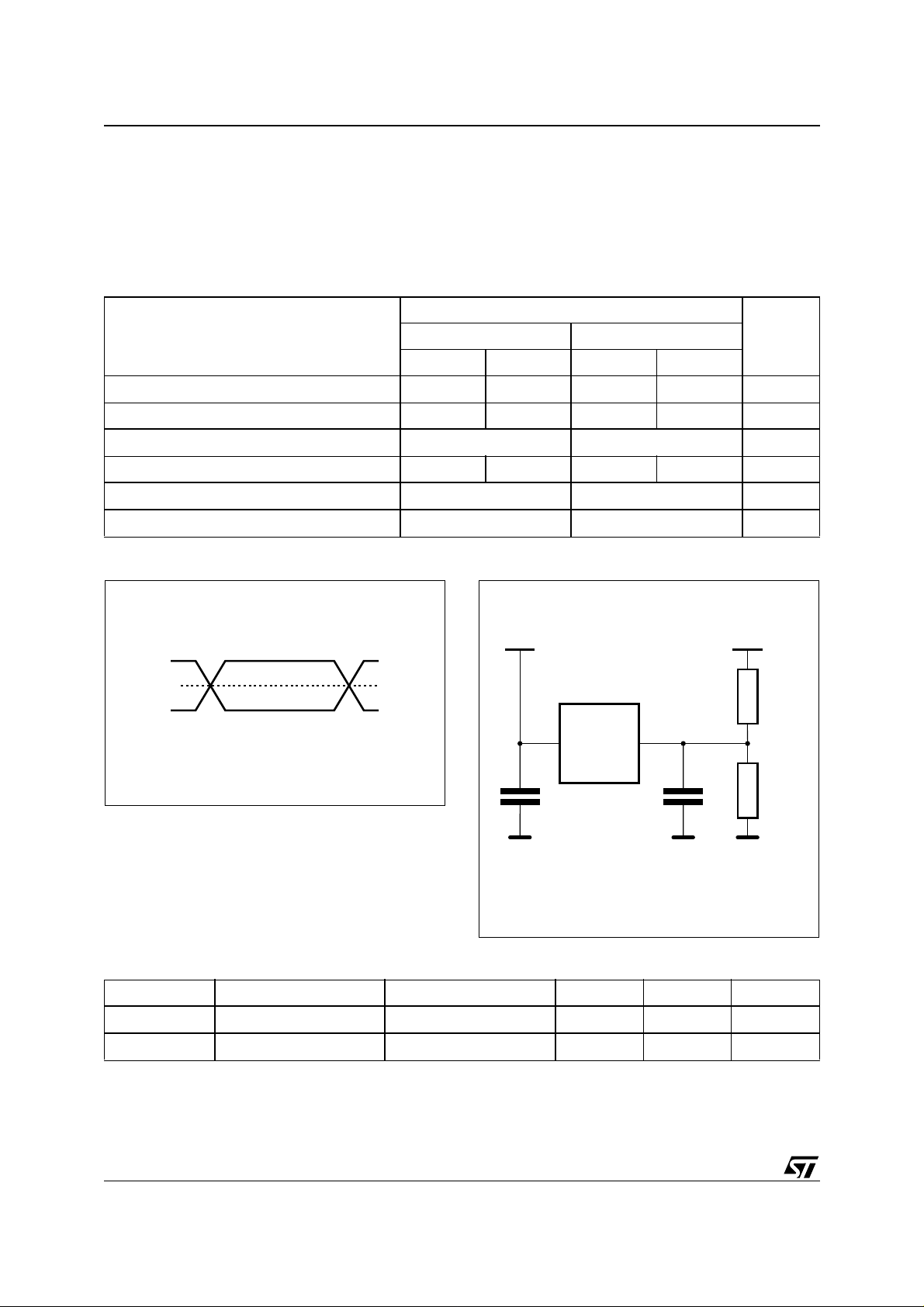
This section summarizes t he operating m easurement conditions, and the DC and AC characteristics of the device. The parameters in the D C and
AC characteristics Tables that follow, are derived
from tests performed under the Measurement
Table 9. Operating and AC Measurement Conditions
Parameter
Min Max Min Max
V
Supply Voltage
CC
Ambient Operating Temperature –40 8 5 –40 85 °C
Conditions summarized in Table 9, Operating and
AC Measurement Conditions. Designers should
check that the operating cond itions in their circuit
match the operating conditions when relying on
the quoted parameters.
M29W160E
2.7 3.6 2.7 3.6 V
Unit70 90
Load Capacitance (C
)
L
30 30 pF
Input Rise and Fall Times 10 10 ns
Input Pulse Voltages
Input and Output Timing Ref. Voltages
0 to V
CC
V
/2 VCC/2
CC
0 to V
CC
Figure 9. AC Measurement I/O Waveform Figure 10. AC Measurement Load Circuit
V
CC
V
CC
VCC/2
0V
AI04498
CL includes JIG capacitance
DEVICE
UNDER
TEST
0.1µF
V
CC
C
L
AI04499
V
V
25kΩ
25kΩ
Table 10. Device Capacitance
Symbol Parameter Test Condition Min Max Unit
V
V
IN
OUT
= 0V
= 0V
6pF
12 pF
C
IN
C
OUT
Note: Sampled only, not 100% test ed.
Input Capacitance
Output Capacitance
20/40
Page 21
M29W160ET, M29W160EB
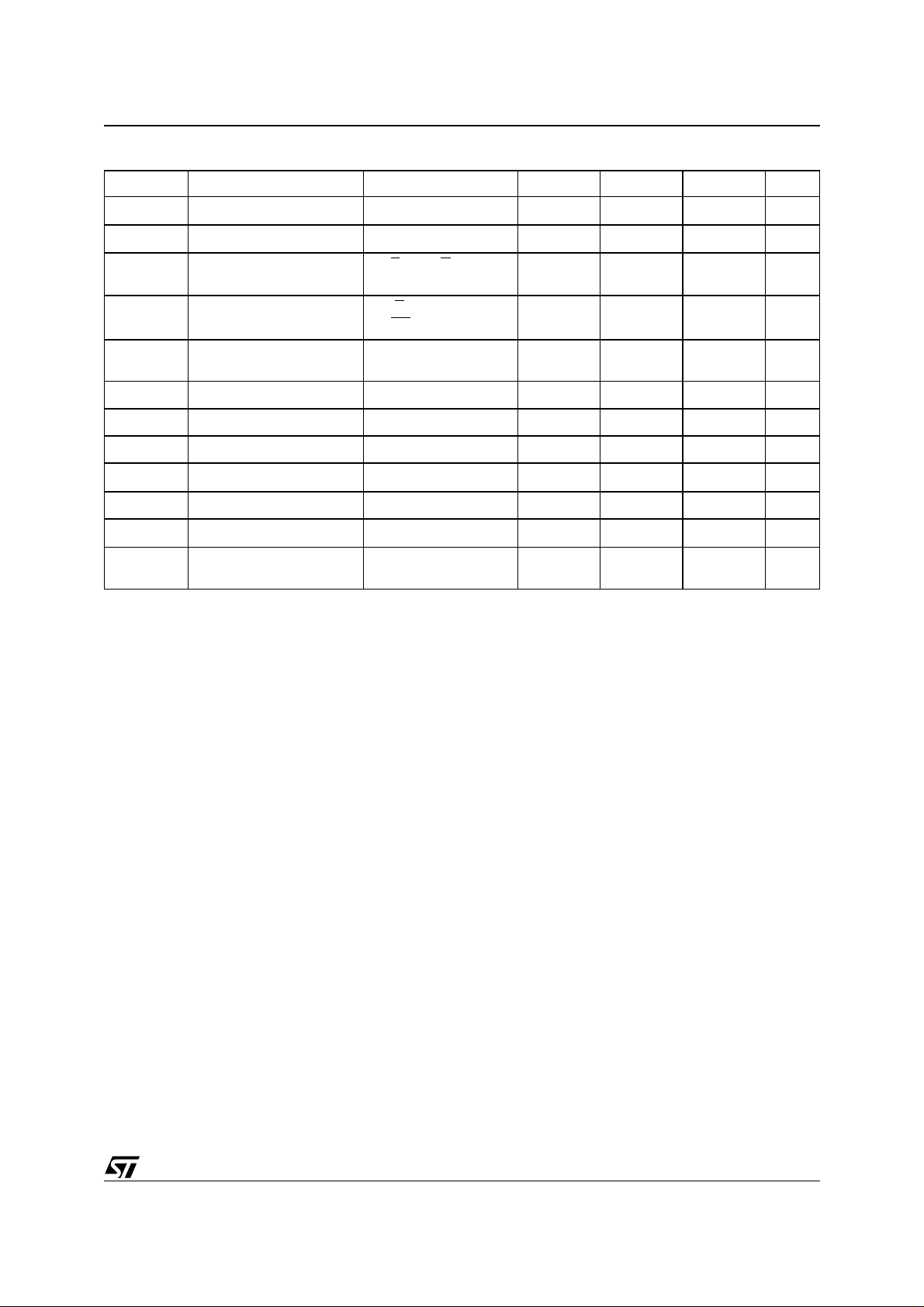
Table 11. DC Characteristics
Symbol Parameter Test Condition Min Typ Max Unit
I
LI
I
LO
I
CC1
I
CC2
I
CC3
V
IL
V
IH
V
OL
V
OH
V
ID
I
ID
V
LKO
Note: 1. Sampled only, not 100% tested.
Input Leakage Current
Output Leakage Curren t
Supply Current (Read)
Supply Current (Standby)
Supply Current
(1)
(Program/Erase)
Input Low Voltage –0.5 0.8 V
Input High Voltage
Output Low Voltage
Output High Voltage IOH = –100µA
Identification Voltage 11.5 12.5 V
Identification Current
Program/Erase Lockout
Supply Voltage
0V
≤ V
≤ V
IN
CC
0V
≤ V
≤ V
OUT
E
= VIL, G = VIH,
f = 6MHz
= VCC ±0.2V,
E
RP
= VCC ±0.2V
Program/Erase
Controller active
I
= 1.8mA
OL
A9 = V
ID
CC
±1
±1
4.5 10 mA
35 100
20 mA
0.7V
CC
VCC +0.3
0.45 V
V
–0.4
CC
100
1.8 2.3 V
µA
µA
µA
V
V
µA
21/40
Page 22
M29W160ET, M29W160EB
Figure 11. Read Mode AC Waveforms
A0-A19/
A–1
tAVQV tAXQX
E
G
DQ0-DQ7/
DQ8-DQ15
tBHQV
BYTE
tAVAV
VALID
tELQV tEHQX
tELQX tEHQZ
tGLQX tGHQX
tGLQV
tGHQZ
VALID
tELBL/tELBH tBLQZ
Table 12. Read AC Characteristics
Symbol Alt Parameter Test Condition
= VIL,
t
AVAV
t
AVQV
(1)
t
ELQX
t
ELQV
(1)
t
GLQX
t
GLQV
(1)
t
EHQZ
(1)
t
GHQZ
t
EHQX
t
GHQX
t
AXQX
t
ELBL
t
ELBH
t
BLQZ
t
BHQV
Note: 1. Sampled only, not 100% tested.
t
RC
t
ACC
t
LZ
t
CE
t
OLZ
t
OE
t
HZ
t
DF
t
OH
t
ELFL
t
ELFH
t
FLQZ
t
FHQV
Address Valid to Next Address Valid
Address Valid to Output Valid
Chip Enable Low to Output Transition
Chip Enable Low to Output Valid
Output Enable Low to Output Transition
Output Enable Low to Output Valid
Chip Enable High to Output Hi-Z
Output Enable High to Output Hi-Z
Chip Enable, Output Enable or Address
Transition to Output Transition
Chip Enable to BYTE Low or High Max 5 5 ns
BYTE Low to Output Hi-Z Max 25 30 ns
BYTE High to Output Valid Max 30 40 ns
E
G
= V
= VIL,
E
G
= V
G
= V
G
= V
E
= V
E
= V
G
= V
E
= V
IL
IL
IL
IL
IL
IL
IL
IL
AI02922
M29W160E
Unit
70 90
Min 70 90 ns
Max 70 90 ns
Min 0 0 ns
Max 70 90 ns
Min 0 0 ns
Max 30 35 ns
Max 25 30 ns
Max 25 30 ns
Min 0 0 ns
22/40
Page 23
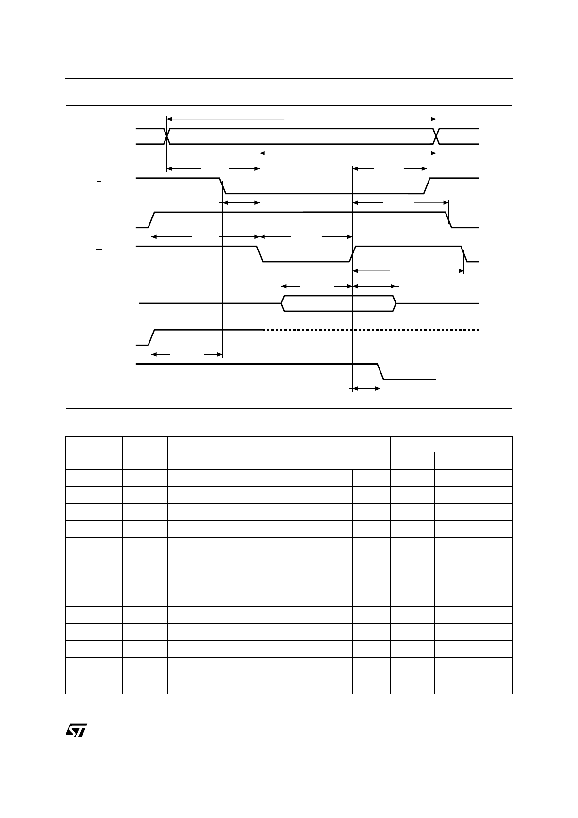
Figure 12. Write AC Waveforms, Write Enable Controlled
tAVAV
A0-A19/
A–1
tAVWL
E
VALID
M29W160ET, M29W160EB
tWLAX
tWHEH
tELWL
G
tWLWHtGHWL
W
tDVWH
DQ0-DQ7/
DQ8-DQ15
V
CC
RB
tVCHEL
VALID
tWHRL
Table 13. Write AC Characteristics, Write Enable Controlled
Symbol Alt Parameter
t
AVAV
t
ELWL
t
WLWH
t
DVWH
t
WHDX
t
WHEH
t
WHWL
t
AVWL
t
WLAX
t
GHWL
t
WHGL
(1)
t
WHRL
t
VCHEL
Note: 1. Sampled only, not 100% tested.
t
WC
t
CS
t
WP
t
DS
t
DH
t
CH
t
WPH
t
AS
t
AH
t
OEH
t
BUSY
t
VCS
Address Valid to Next Address Valid Min 70 90 ns
Chip Enable Low to Write Enable Low Min 0 0 ns
Write Enable Low to Write Enable High Min 45 50 ns
Input Valid to Write Enable High Min 45 50 ns
Write Enable High to Input Transition Min 0 0 ns
Write Enable High to Chip Enable High Min 0 0 ns
Write Enable High to Write Enable Low Min 30 30 ns
Address Valid to Write Enable Low Min 0 0 ns
Write Enable Low to Address Transition Min 45 50 ns
Output Enable High to Write Enable Low Min 0 0 ns
Write Enable High to Output Enable Low Min 0 0 ns
Program/Erase Valid to RB Low Max 30 35 ns
VCC High to Chip Enable Low
tWHGL
tWHWL
tWHDX
AI02923
M29W160E
Unit
70 90
Min 50 50 µs
23/40
Page 24
M29W160ET, M29W160EB
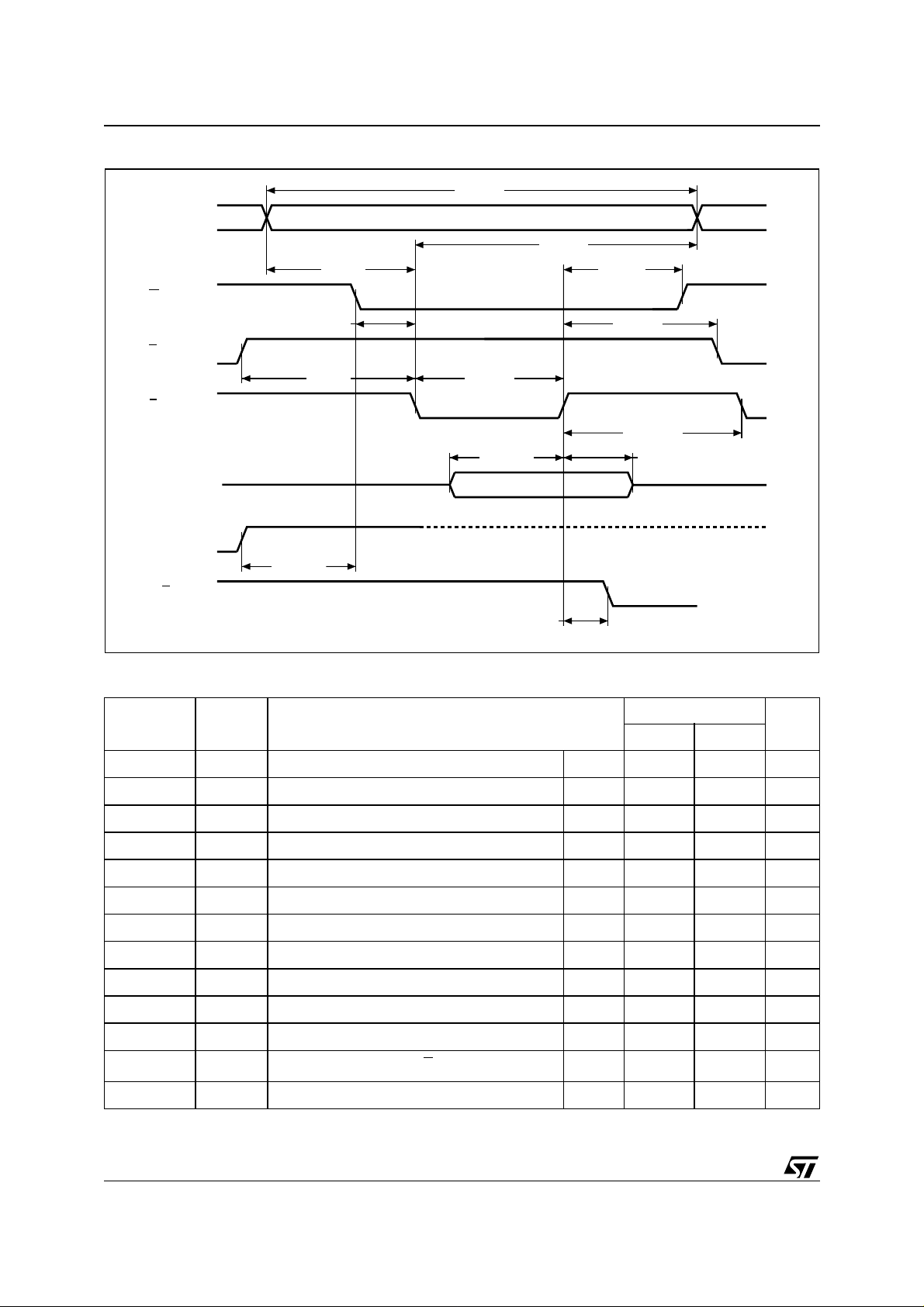
Figure 13. Write AC Waveforms, Chip Enable Controlled
tAVAV
A0-A19/
A–1
tAVEL
W
VALID
tELAX
tEHWH
tWLEL
G
tELEHtGHEL
E
tDVEH
DQ0-DQ7/
DQ8-DQ15
V
CC
RB
tVCHWL
VALID
tEHRL
Table 14. Write AC Characteristics, Chip Enable Controlled
Symbol Alt Parameter
t
AVAV
t
WLEL
t
ELEH
t
DVEH
t
EHDX
t
EHWH
t
EHEL
t
AVEL
t
ELAX
t
GHEL
t
EHGL
(1)
t
EHRL
t
VCHWL
Note: 1. Sampled only, not 100% tested.
t
WC
t
WS
t
CP
t
DS
t
DH
t
WH
t
CPH
t
AS
t
AH
t
OEH
t
BUSY
t
VCS
Address Valid to Next Address Valid Min 70 90 ns
Write Enable Low to Chip Enable Low Min 0 0 ns
Chip Enable Low to Chip Enable High Min 45 50 ns
Input Valid to Chip Enable High Min 45 50 ns
Chip Enable High to Input Transition Min 0 0 ns
Chip Enable High to Write Enable High Min 0 0 ns
Chip Enable High to Chip Enable Low Min 30 30 ns
Address Valid to Chip Enable Low Min 0 0 ns
Chip Enable Low to Address Transition Min 45 50 ns
Output Enable High Chip Enable Low Min 0 0 ns
Chip Enable High to Output Enable Low Min 0 0 ns
Program/Erase Valid to RB Low Max 30 35 ns
VCC High to Write Enable Low
tEHGL
tEHEL
tEHDX
AI02924
M29W160E
Unit
70 90
Min 50 50 µs
24/40
Page 25
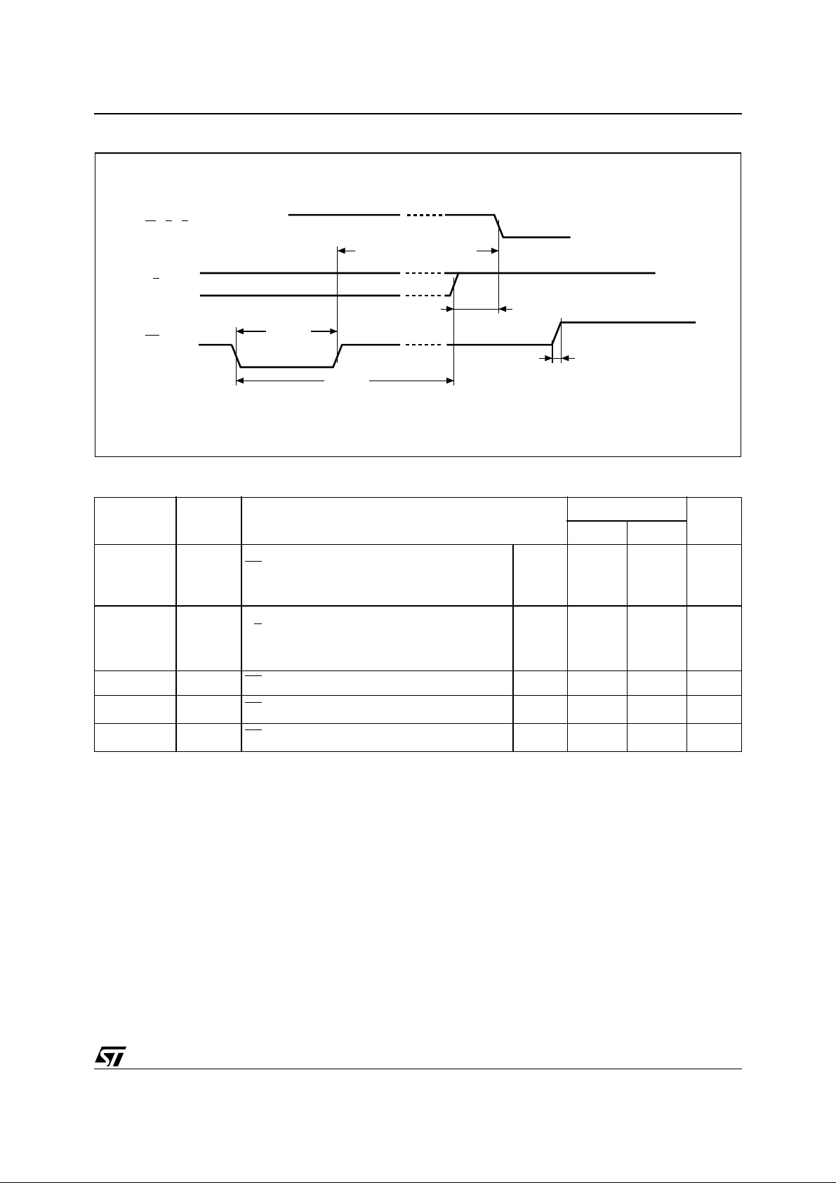
Figure 14. Reset/Block Temporary Unprotect AC Waveforms
E, G
W,
tPHWL, tPHEL, tPHGL
RB
RP
tPLPX
tPLYH
Table 15. Reset/Block Temporary Unprotect AC Characteristics
Symbol Alt Parameter
(1)
t
PHWL
t
PHEL
(1)
t
PHGL
(1)
t
RHWL
(1)
t
RHEL
(1)
t
RHGL
t
PLPX
(1)
t
PLYH
(1)
t
PHPHH
Note: 1. Sampled only, not 100% tested.
t
RH
t
RB
t
RP
t
READY
t
VIDR
RP High to Write Enable Low, Chip Enable Low,
Output E nable Low
RB High to Write Enable Low, Chip Enable Low,
Output E nable Low
RP Pulse Width Min 500 500 ns
RP Low to Read Mode Max 10 10 µs
RP Rise Time to V
ID
M29W160ET, M29W160EB
tRHWL, tRHEL, tRHGL
tPHPHH
AI02931B
M29W160E
Unit
70 90
Min 50 50 ns
Min 0 0 ns
Min 500 500 ns
25/40
Page 26
M29W160ET, M29W160EB
PACKAGE MECHANICAL
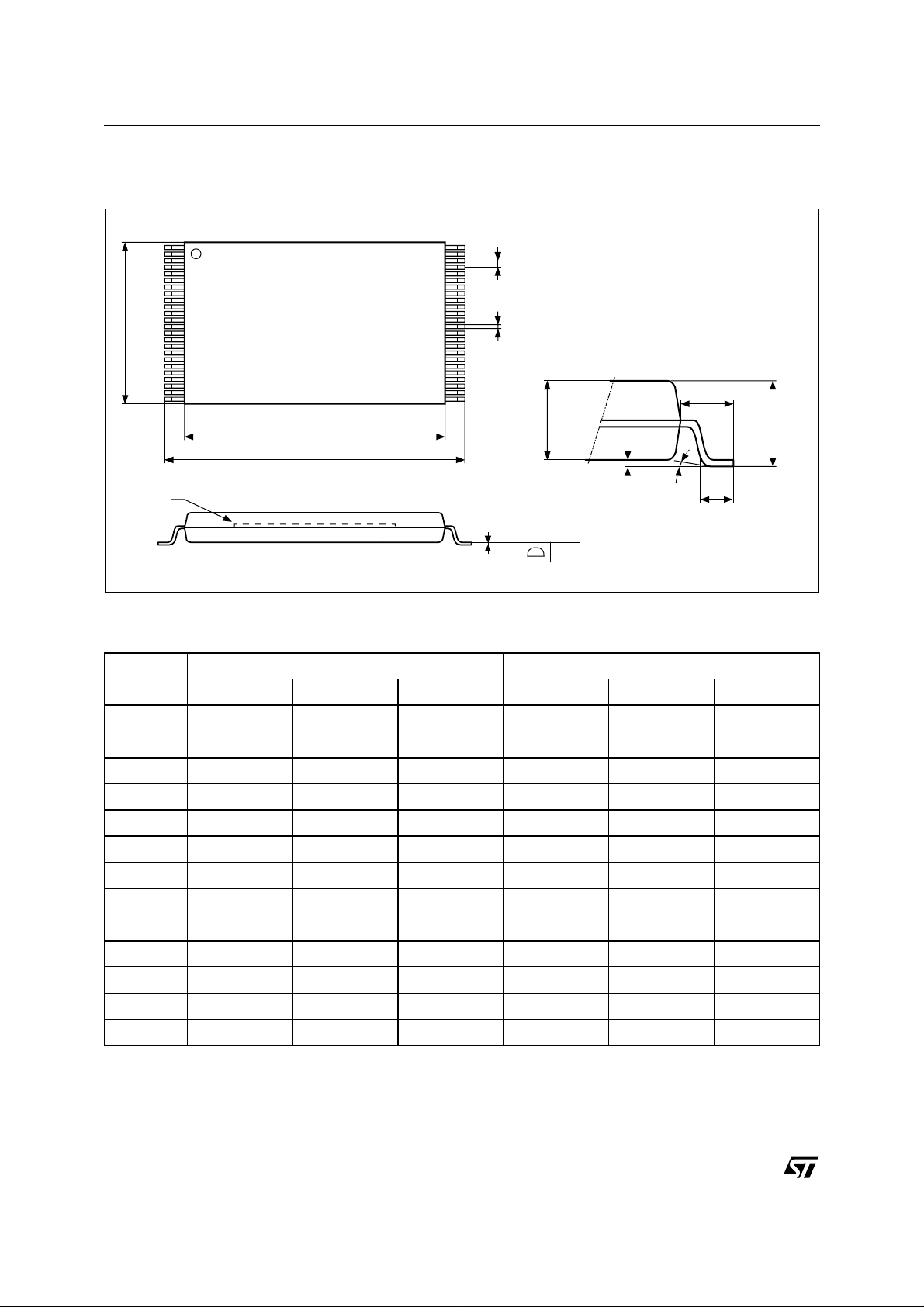
Figure 15. TSOP48 – 48 lead Plastic Thin Small Outline, 12 x 20mm, Pa ckage Outline
1
48
e
D1
24
E1
B
25
L1
A2
E
DIE
LA1 α
C
CP
Note: Drawing is not to scale.
TSOP-G
Table 16. TSOP48 – 48 lead Plastic Thin Small Outline, 12 x 20mm, Package Mechan ical Data
Symbol
Typ Min Max Typ Min Max
A 1.200 0.0472
millimeters inches
A
A1 0.100 0.050 0.150 0.0039 0.0020 0.0059
A2 1.000 0.950 1.050 0.0394 0.0374 0.0413
B 0.220 0.170 0.270 0.0087 0.0067 0.0106
C 0.100 0.210 0.0039 0.0083
CP 0.080 0.0031
D1 12.000 11.900 12.100 0.4724 0.4685 0.4764
E 20.000 19.800 20.200 0.7874 0.7795 0.7953
E1 18.400 18.300 18.500 0.7244 0.7205 0.7283
e 0.500 – – 0.0197 – –
L 0.600 0.500 0.700 0.0236 0.0197 0.0276
L1 0.800 0.0315
α 305305
26/40
Page 27
M29W160ET, M29W160EB
Figure 16. TFBGA48 6x8mm - 6x8 ball array, 0.80 mm pitch, Package Outline
D
D1
SD
SE
e
A2
A1
FE
E1E
FD
BALL "A1"
eb
A
ddd
BGA-Z32
Table 17. TFBGA48 6x8mm - 6x8 ball array, 0.80 mm pitch, Package Mechanical Data
Symbol
Typ Min Max Typ Min Max
A 1.200 0.0472
A1 0.260 0.0102
A2 0.900 0.0354
b 0.350 0.450 0.0138 0.0177
D 6.000 5.900 6.100 0.2362 0.2323 0.2402
D1 4.000 – – 0.1575 – –
ddd 0.100 0.0039
E 8.000 7.900 8.100 0.3150 0.3110 0.3189
E1 5.600 – – 0.2205 – –
e 0.800 – – 0.0315 – –
FD 1.000 – – 0.0394 – –
millimeters inches
FE 1.200 – – 0.0472 – –
SD 0.400 – – 0.0157 – –
SE 0.400 – – 0.0157 – –
27/40
Page 28

M29W160ET, M29W160EB
PART NUMBERING
Table 18. Ordering Information Scheme
Example: M29W160EB 90 N 6 T
Device Type
M29
Operating Voltage
W = V
Device Function
160E = 16 Mbit (x8/x16), Boot Block
Array Matrix
T = Top Boot
B = Bottom Boot
Speed
70 = 70 ns
90 = 90 ns
= 2.7 to 3.6V
CC
Package
N = TSOP48: 12 x 20 mm
ZA = TFBGA48: 6x8 mm, 0.80mm pitch
Temperature Range
6 = –40 to 85 °C
Option
Blank = Standard Packing
T = Tape and Reel Packing
E = Lead-free Package, Standard Packing
F = Lead-free Package, Tape & Reel Packing
Devices are shipped from the factory with the memory content bits erased to ’1’.
For a list of available options (Speed, Package, etc.) or for further information on any aspect of this device,
please contact the ST Sales Office nearest to you.
28/40
Page 29
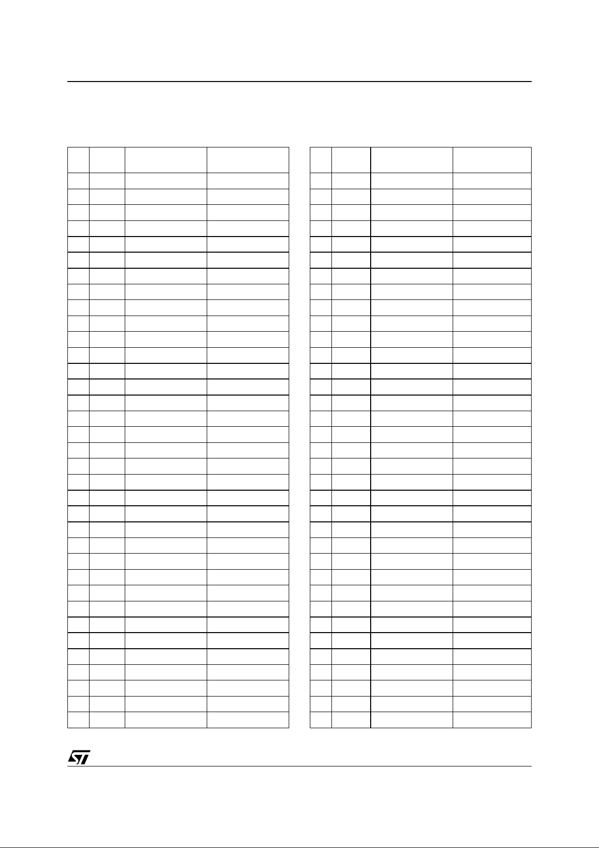
APPENDIX A. BLOCK ADDRESS TABLE
M29W160ET, M29W160EB
Table 19. Top Boot Block Addresses,
M29W160ET
Size
#
(KBytes)
34 16 1FC000h-1FFFFFh FE000h-FFFFFh
33 8 1FA000h-1FBFFFh FD000h-FDFFFh
32 8 1F8000h-1F9FFFh FC000h-FCFFFh
31 32 1F0000h-1F7FFFh F8000h-FBFFFh
30 64 1E0000h-1EFFFFh F0000h-F7FFFh
29 64 1D0000h-1DFFFFh E8000h-EFFFFh
28 64 1C0000h-1CFFFFh E0000h-E7FFFh
27 64 1B0000h-1BFFFFh D8000h-DFFFFh
26 64 1A0000h-1AFFFFh D0000h-D7FFFh
25 64 190000h-19FFFFh C8000h-CFFFFh
24 64 180000h-18FFFFh C0000h-C7FFFh
23 64 170000h-17FFFFh B8000h-BFFFFh
22 64 160000h-16FFFFh B0000h-B7FFFh
21 64 150000h-15FFFFh A8000h-AFFFFh
20 64 140000h-14FFFFh A0000h-A7FFFh
19 64 130000h-13FFFFh 98000h-9FFFFh
18 64 120000h-12FFFFh 90000h-97FFFh
17 64 110000h-11FFFFh 88000h-8FFFFh
16 64 100000h-10FFFFh 80000h-87FFFh
15 64 0F0000h-0FFFFFh 78000h-7FFFFh
14 64 0E0000h-0EFFFFh 70000h-77FFFh
13 64 0D0000h-0DFFFFh 68000h-6FFFFh
12 64 0C0000h-0CFFFFh 60000h-67FFFh
11 64 0B0000h-0BFFFFh 58000h-5FFFFh
10 64 0A0000h-0AFFFFh 50000h-57FFFh
9 64 090000h-09FFFFh 48000h-4FFFFh
8 64 080000h-08FFFFh 40000h-47FFFh
7 64 070000h-07FFFFh 38000h-3FFFFh
6 64 060000h-06FFFFh 30000h-37FFFh
5 64 050000h-05FFFFh 28000h-2FFFFh
4 64 040000h-04FFFFh 20000h-27FFFh
3 64 030000h-03FFFFh 18000h-1FFFFh
2 64 020000h-02FFFFh 10000h-17FFFh
1 64 010000h-01FFFFh 08000h-0FFFFh
0 64 000000h-00FFFFh 00000h-07FFFh
Addres s Range
(x8)
Address Ran ge
(x16)
Table 20. Bottom Boot Block Addresses,
M29W160EB
Size
#
(KBytes)
34 64 1F0000h-1FFFFFh F8000h-FFFFFh
33 64 1E0000h-1EFFFFh F0000h-F7FFFh
32 64 1D0000h-1DFFFFh E8000h-EFFFFh
31 64 1C0000h-1CFFFFh E0000h-E7FFFh
30 64 1B0000h-1BFFFFh D8000h-DFFFFh
29 64 1A0000h-1AFFFFh D0000h-D7FFFh
28 64 190000h-19FFFFh C8000h-CFFFFh
27 64 180000h-18FFFFh C0000h-C7FFFh
26 64 170000h-17FFFFh B8000h-BFFFFh
25 64 160000h-16FFFFh B0000h-B7FFFh
24 64 150000h-15FFFFh A8000h-AFFFFh
23 64 140000h-14FFFFh A0000h-A7FFFh
22 64 130000h-13FFFFh 98000h-9FFFFh
21 64 120000h-12FFFFh 90000h-97FFFh
20 64 110000h-11FFFFh 88000h-8FFFFh
19 64 100000h-10FFFFh 80000h-87FFFh
18 64 0F0000h-0FFFFFh 78000h-7FFFFh
17 64 0E0000h-0EFFFFh 70000h-77FFFh
16 64 0D0000h-0DFFFFh 68000h-6FFFFh
15 64 0C0000h-0CFFFFh 60000h-67FFFh
14 64 0B0000h-0BFFFFh 58000h-5FFFFh
13 64 0A0000h-0AFFFFh 50000h-57FFFh
12 64 090000h-09FFFFh 48000h-4FFFFh
11 64 080000h-08FFFFh 40000h-47FFFh
10 64 070000h-07FFFFh 38000h-3FFFFh
9 64 060000h-06FFFFh 30000h-37FFFh
8 64 050000h-05FFFFh 28000h-2FFFFh
7 64 040000h-04FFFFh 20000h-27FFFh
6 64 030000h-03FFFFh 18000h-1FFFFh
5 64 020000h-02FFFFh 10000h-17FFFh
4 64 010000h-01FFFFh 08000h-0FFFFh
3 32 008000h-00FFFFh 04000h-07FFFh
2 8 006000h-007FFFh 03000h-03FFFh
1 8 004000h-005FFFh 02000h-02FFFh
0 16 000000h-003FFFh 00000h-01FFFh
Address Range
(x8)
Address Range
(x16)
29/40
Page 30
M29W160ET, M29W160EB
APPENDIX B. COMMON FLASH INTERFACE (CFI)
The Common Flash Interface is a JEDEC approved, standardized data structure that can be
read from the Flash memory device. It allows a
system software to query the device to det ermine
various electrical and timing p arameters, density
information and functions su pported by the memory. The system can interface easily with the device, enabling the software to upgrade itself when
necessary.
When the CFI Query Command is issued the device enters CFI Query mode and the data structure
is read from the memory. Tables 21, 22, 23, 24, 25
Table 21. Query Structure Overview
Address
x16 x8
10h 20h CFI Query Identification String Command set ID and algorithm data offset
1Bh 36h System Interface Information Device timing & voltage information
27h 4Eh Device Geometry Definition Flash device layout
40h 80h
61h C2h Security Code Area 64 bit unique device number
Note: Query data are always pr esented on the lowest or der data outputs.
Primary Algorithm-specific Extended
Query table
Sub-section Name Description
and 26 show the addres ses used to retrieve the
data.
The CFI data structure also contains a security
area where a 64 bit unique security number is written (see Table 26, Security Code area). This area
can be accessed only in Read mode by the final
user. It is impossible to change the security num ber after it has been written by ST. Issue a Read
command to return to Read mode.
Note: The Common Fl ash Interface is only available for Temperature range 6 (–40 to 85°C).
Additional information specific to the Primary
Algorithm (optional)
Table 22. CFI Query Identification String
Address
x16 x8
10h 20h 0051h "Q"
11h 22h 0052h Query Unique ASCII String "QRY" "R"
12h 24h 0059h "Y"
13h 26h 0002h
14h 28h 0000h
15h 2Ah 0040h
16h 2Ch 0000h
17h 2Eh 0000h
18h 30h 0000h
19h 32h 0000h
1Ah 34h 0000h
Note: Query data are always presented on the lowest order data outputs (DQ7-DQ0) only. DQ8-DQ15 are ‘0’.
Data Description Value
Primary Algorithm Command Set and Control Interface ID code 16 bit
ID code defining a specific algorithm
Address for Primary Algorithm extended Query table (see Table 24) P = 40h
Alternate Vendor Command Set and Control Interface ID Code second
vendor - specified algorithm supported
Address for Alternate Algorithm extended Query table
AMD
Compatible
NA
NA
30/40
Page 31
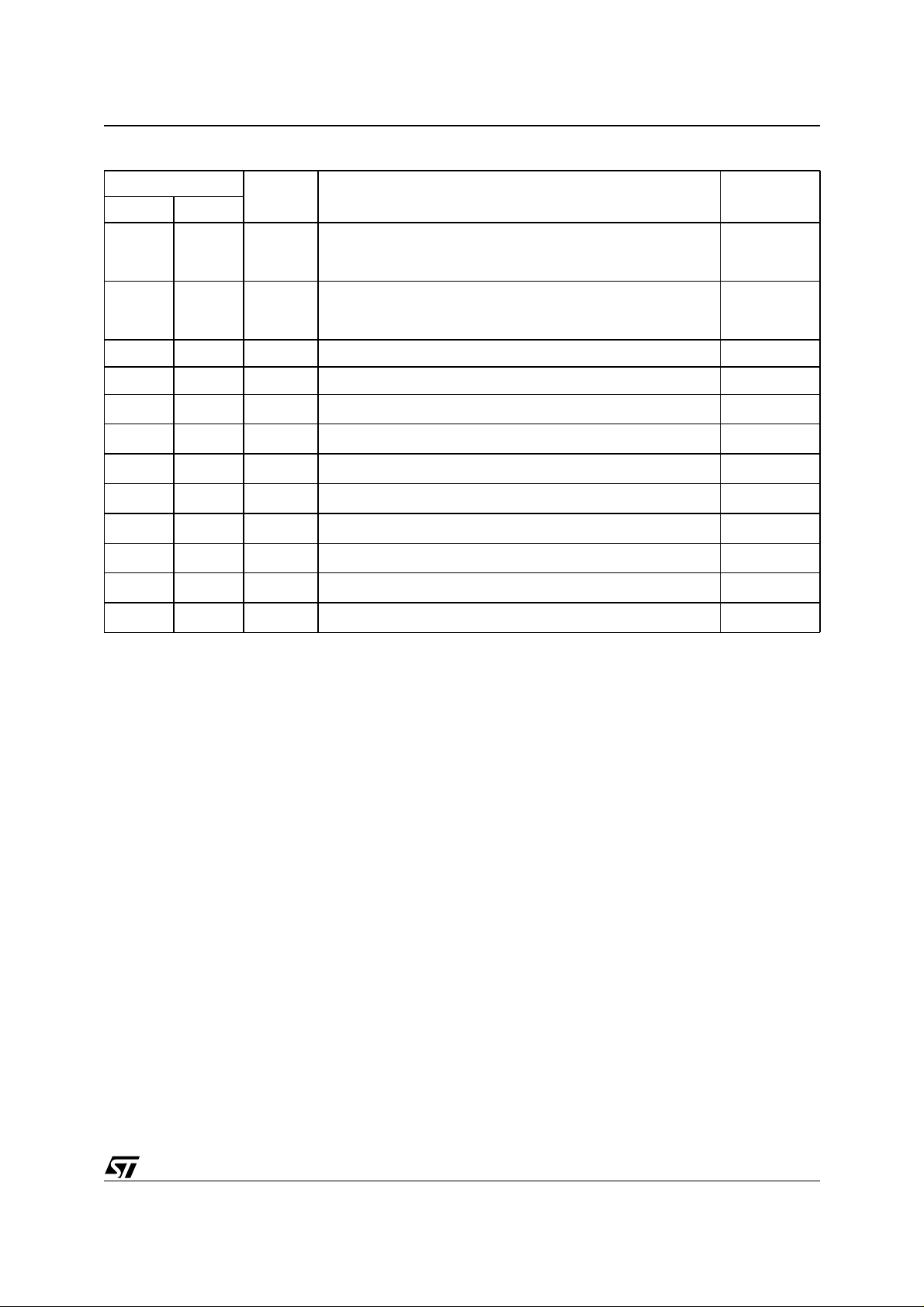
Table 23. CFI Query System Interface Information
Address
x16 x8
1Bh 36h 0027h
1Ch 38h 0036h
1Dh 3Ah 0000h
1Eh 3Ch 0000h
1Fh 3Eh 0004h
20h 40h 0000h
21h 42h 000Ah
22h 44h 0000h
23h 46h 0004h
24h 48h 0000h
25h 4Ah 0003h
26h 4Ch 0000h
Data Description Value
V
Logic Supply Minimum Program/Erase voltage
CC
bit 7 to 4BCD value in volts
bit 3 to 0BCD value in 100 mV
V
Logic Supply Maximum Program/Erase voltage
CC
bit 7 to 4BCD value in volts
bit 3 to 0BCD value in 100 mV
V
[Programming] Supply Minimum Program/Erase voltage
PP
V
[Programming] Supply Maximum Program/Erase voltage
PP
Typical timeout per single Byte/Word program = 2
Typical timeout for minimum size write buffer program = 2
Typical timeout per individual block erase = 2
Typical timeout for full chip erase = 2
Maximum timeout for Byte/Word program = 2
Maximum timeout for write buffer program = 2
Maximum timeout per individual block erase = 2
Maximum timeout for chip erase = 2
n
ms
n
ms
n
times typical
n
n
times typical
M29W160ET, M29W160EB
2.7V
3.6V
NA
NA
n
µs
n
µs
times typical
n
times typical
16µs
NA
1s
NA
256µs
NA
8s
NA
31/40
Page 32
M29W160ET, M29W160EB
Table 24. Device Geometry Definition
Address
x16 x8
27h 4Eh 0015h
Data Description Value
Device Size = 2
n
in number of Bytes
2 MByte
28h
29h
2Ah
2Bh
2Ch 58h 0004h
2Dh
2Eh
2Fh
30h
31h
32h
33h
34h
35h
36h
37h
38h
39h
3Ah
3Bh
3Ch
50h
52h
54h
56h
5Ah
5Ch
5Eh
60h
62h
64h
66h
68h
6Ah
6Ch
6Eh
70h
72h
74h
76h
78h
0002h
0000h
0000h
0000h
0000h
0000h
0040h
0000h
0001h
0000h
0020h
0000h
0000h
0000h
0080h
0000h
001Eh
0000h
0000h
0001h
Flash Device Interface Code description
Maximum number of Bytes in multi-Byte program or page = 2
Number of Erase Block Regions within the device.
It specifies the number of regions within the device containing
contiguous Erase Blocks of the same size.
Region 1 Information
Number of identical size erase block = 0000h+1
Region 1 Information
Block size in Region 1 = 0040h * 256 Byte
Region 2 Information
Number of identical size erase block = 0001h+1
Region 2 Information
Block size in Region 2 = 0020h * 256 Byte
Region 3 Information
Number of identical size erase block = 0000h+1
Region 3 Information
Block size in Region 3 = 0080h * 256 Byte
Region 4 Information
Number of identical-size erase block = 001Eh+1
Region 4 Information
Block size in Region 4 = 0100h * 256 Byte
x8, x16
Async.
n
NA
4
1
16 KByte
2
8 KByte
1
32 KByte
31
64 KByte
32/40
Page 33
Table 25. Primary Algorithm-Specific Extended Qu ery Ta ble
Address
Data Description Value
x16 x8
M29W160ET, M29W160EB
40h 80h 0050h
41h 82h 0052h "R"
42h 84h 0049h "I"
43h 86h 0031h Major version number, ASCII "1"
44h 88h 0030h Minor version number, ASCII "0"
45h 8Ah 0000h Address Sensitive Unlock (bits 1 to 0)
46h 8Ch 0002h Erase Suspend
47h 8Eh 0001h Block Protection
48h 90h 0001h Temporary Block Unprotect
49h 92h 0004h Block Protect /Unprotect
4Ah 94h 0000h Simultaneous Operations, 00 = not supported No
4Bh 96h 0000h Burst Mode, 00 = not supported, 01 = supported No
4Ch 98h 0000h Page Mode, 00 = not supported, 01 = 4 page Word, 02 = 8 page Word No
Primary Algorithm extended Query table unique ASCII string “PRI”
00 = required, 01= not required
Silicon Revision Number (bits 7 to 2)
00 = not supported, 01 = Read only, 02 = Read and Write
00 = not supported, x = number of blocks in per group
00 = not supported, 01 = supported
04 = M29W400B
"P"
Yes
2
1
Yes
4
Table 26. Security Code Area
Address
x16 x8
61h C3h, C2h XXXX
62h C5h, C4h XXXX
63h C7h, C6h XXXX
64h C9h, C8h XXXX
Data Description
64 bit: unique device number
33/40
Page 34
M29W160ET, M29W160EB
APPENDIX C. BLOCK PROTECTION
Block protection can be used to prevent any operation from modifying the data stored in the Flash
memory. Each Block can be protected individually.
Once protected, Program and Erase operations
on the block fail to change the data.
There are three techniques that can be used to
control Block Protection, these are the Programmer technique, the In-System technique and Temporary Unprotection. Temporary Unprotection is
controlled by the Reset/Block Temporary Unprotection pin, RP
scriptions section.
Unlike the Command Interface of the Program/
Erase Controller, the techniques for protecting and
unprotecting blocks could change between different Flash memory suppliers.
Programm er Te chnique
The Programmer techniq ue uses high (V
age levels on some of the bus pins. These cannot
be achieved using a standard microprocessor bus,
therefore the technique is recommended on ly for
use in Programming Equipment.
To protect a block follow the flowchart in Figure 17,
Programmer Equipment Block Protec t Flowchart.
During the Block Protect algorithm, the A19-A12
Address Inputs indicate the address of the block to
be protected. The block will be correctly protected
only if A19-A12 remain valid and stable, and if
Chip Enable is kept Low, V
and Verify phases.
The Chip Unprotect algorithm is used to unprotect
all the memory blocks at the same time. This algorithm can only be used if all of t he bl ocks are protected first. To unprotect the chip follow Figure 18,
; this is described in the Signal De-
) volt-
ID
, all along the Protect
IL
Programmer Equipment Chip Unprotect Flowchart. Table 27, Programmer Technique Bus Operations, gives a summary of each operation.
The timing on these flowcharts is critical. Care
should be taken t o ensure t hat, where a pause is
specified, it is followed as closely as possible. Do
not abort the procedure be fore reaching the end.
Chip Unprotect can take several seconds and a
user message should be provided to show that the
operation is progressing.
In-System Technique
The In-System technique requires a high voltage
level on the Reset/Blocks Temporary Unprotect
pin, RP
. This can be achieved without violating the
maximum ratings of the components on the microprocessor bus, therefore this technique is suitable
for use after the Flash memory has been fitted to
the system.
To protect a block follow the flowchart in Figure 19,
In-System Block Protect Flowchart. To unprot ect
the whole chip it is necessary to protect all of the
blocks first, then all the blocks can be unprotected
at the same time. To unprotect the chip follow Figure 20, In-System Chip Unprotect Flowchart.
The timing on these flowcharts is critical. Care
should be taken t o ensure t hat, where a pause is
specified, it is followed as closely as possible. Do
not allow the microprocessor to serv ice interrupts
that will upset the timing and do not abort the procedure before reaching t he end. Chip Unprotect
can take several seconds and a user message
should be provided to show that the operation is
progressing.
Table 27. Programmer Technique Bus Op erati ons, BYTE
Operation E G W
Block Protect
Chip Unprotect
Block Protection
Verify
Block Unprotection
Verify
34/40
V
IL
V
IDVIDVIL
V
IL
V
IL
VIDVIL Pulse
Pulse
V
V
V
IL
IL
IH
V
IH
A9 = V
A0 = VIL, A1 =VIH, A6 = VIL, A9 = VID,
A0 = VIL, A1 = VIH, A6 =VIH, A9 = VID,
Address Inputs
A0-A19
, A12-A19 Block Address
ID
Others = X
A9 = V
, A12 = VIH, A15 = VIH
ID
Others = X
A12-A19 Block Address
Others = X
A12-A19 Block Address
Others = X
= VIH or V
IL
Data Inputs/Outputs
DQ15A–1, DQ14 -DQ0
X
X
Pass = XX01h
Retry = XX00h
Retry = XX01h
Pass = XX00h
Page 35
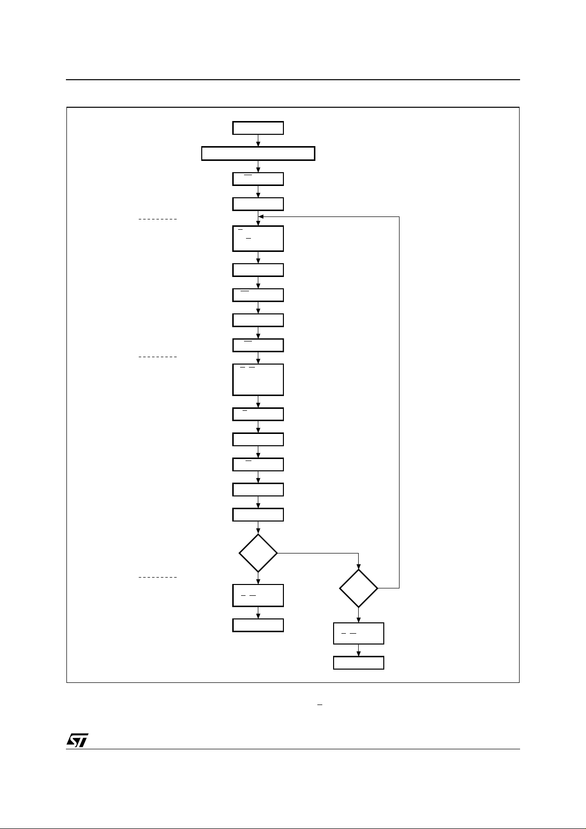
Figure 17. Programmer Equipment Bl oc k P rot ect Flowchart
START
ADDRESS = BLOCK ADDRESS
W = V
IH
n = 0
G, A9 = VID,
E = V
IL
Wait 4µs
(1)
W = V
IL
Wait 100µs
W = V
IH
M29W160ET, M29W160EB
Verify Protect Set-upEnd
E, G = VIH,
A0, A6 = VIL,
A1 = V
IH
(1)
E = V
IL
Wait 4µs
G = V
IL
Wait 60ns
Read DATA
DATA
=
01h
YES
A9 = V
IH
E, G = V
IH
PASS
NO
++n
= 25
A9 = V
E, G = V
NO
YES
IH
IH
FAIL
Note: 1. Address In puts A1 9-A12 g ive the a ddres s of th e bloc k t hat is to be pr ot ecte d. I t is imp era tive t hat they rem ain st able d urin g the
operation.
2. During the Protect and Verify phases of the algorithm, Chip Enable E
must be kept Low, VIL.
AI03469b
35/40
Page 36
M29W160ET, M29W160EB
Figure 18. Programmer Equipment Chip Unprotect Flowchart
START
PROTECT ALL BLOCKS
CURRENT BLOCK = 0
ADDRESS = CURRENT BLOCK ADDRESS
n = 0
A6, A12, A15 = V
E, G, A9 = V
Wait 4µs
W = V
Wait 10ms
W = V
E, G = V
A0 = VIL, A1, A6 = V
E = V
Wait 4µs
IH
ID
IL
IH
IH
IL
(1)
IH
36/40
Verify Unprotect Set-upEnd
G = V
IL
Wait 60ns
Read DATA
=
00h
YESNO
DATA
++n
NO
= 1000
YES
A9 = V
IH
E, G = V
IH
FAIL PASS
CURRENT BLOCK
LAST
BLOCK
YES
A9 = V
IH
E, G = V
IH
INCREMENT
NO
AI03470
Page 37
Figure 19. In-System Equipment Block Protect Flowchart
START
n = 0
RP = V
ID
M29W160ET, M29W160EB
Verify Protect Set-upEnd
ADDRESS = BLOCK ADDRESS
ADDRESS = BLOCK ADDRESS
ADDRESS = BLOCK ADDRESS
ADDRESS = BLOCK ADDRESS
A0 = VIL, A1 = VIH, A6 = V
WRITE 60h
A0 = VIL, A1 = VIH, A6 = V
WRITE 60h
A0 = VIL, A1 = VIH, A6 = V
Wait 100µs
WRITE 40h
A0 = VIL, A1 = VIH, A6 = V
Wait 4µs
READ DATA
DATA
RP = V
01h
NO
=
YES
IH
IL
IL
IL
IL
++n
= 25
NO
ISSUE READ/RESET
COMMAND
PASS
YES
RP = V
IH
ISSUE READ/RESET
COMMAND
FAIL
AI03471
37/40
Page 38
M29W160ET, M29W160EB
Figure 20. In-System Equipment Chip Unprotect Flowchart
START
PROTECT ALL BLOCKS
Verify Unprotect Set-upEnd
CURRENT BLOCK = 0
A0 = VIL, A1 = VIH, A6 = V
A0 = VIL, A1 = VIH, A6 = V
ADDRESS = CURRENT BLOCK ADDRESS
A0 = VIL, A1 = VIH, A6 = V
ADDRESS = CURRENT BLOCK ADDRESS
A0 = VIL, A1 = VIH, A6 = V
n = 0
RP = V
ID
WRITE 60h
ANY ADDRESS WITH
WRITE 60h
ANY ADDRESS WITH
Wait 10ms
WRITE 40h
Wait 4µs
READ DATA
IH
IH
IH
IH
INCREMENT
CURRENT BLOCK
38/40
++n
NO
= 1000
YES
RP = V
IH
ISSUE READ/RESET
COMMAND
FAIL
DATA
=
00h
YESNO
LAST
BLOCK
RP = V
ISSUE READ/RESET
COMMAND
PASS
NO
YES
IH
AI03472
Page 39
M29W160ET, M29W160EB
REVISION HIST ORY
Table 28. Document Revision History
Date Version Revision Details
06-Aug-2002 -01 First Issue: originates from M29W160D datasheet dated 24-Jun-2002
9x8mm FBGA48 package replaced by 6x8mm. VDD(min) reduced for -70ns speed class.
27-Nov-2002 1.1
03-Dec-2002 1.2 Package information corrected in ordering information table.
21-Mar-2003 2.0
27-Jun-2003 2.1 TSOP48 package information updated (see Figure 15 and Table 16).
26-Jan-2004 3.0 Block Erase Command clarified.
Erase Suspend Latency Time (typical and maximum) added to Program, Erase Times
and Program, Erase Endurance Cycles table. Logic Diagram corrected.
Document promoted to full Datasheet status. Block Protect and Chip Unprotect
algorithms specified in Appendix C, BLOCK PROTECTION.
39/40
Page 40

M29W160ET, M29W160EB
Information furnished i s believed to be accurate and reliable. However, STMicroe lectronics assumes no respons ibili ty for the consequences of use of such
information nor for any infri ngement of patents or other rights of third p arties which m ay result from i ts use. No l icense is granted by implic ation or oth erwise
under any patent or pat ent ri ghts of STMi croel ect ronic s. Specifi cations me ntion ed i n thi s publ icat ion ar e s ubj ect to change without notice. This publication
supersedes and r eplaces a ll i nform atio n pr eviously s uppl i ed. STMi croel ectr onics pr oduc ts are not a uthori zed f or use as cr iti cal com ponents i n l if e s upport
devices or systems without express written approval of STMicroelectronics.
The ST logo is a registered trademark of STMicroelectronics.
All other names are the property of their respective owners.
© 2004 STMicroelectronics - All rights reserved
Australia - Belgium - Brazil - Canada - China - Czech Republic - Finland - France - Germany -
Hong Kong - India - Israel - Italy - Japan - Malaysia - Malta - Morocco - Singapore -
STMicroelectronics GROUP OF COMPANIES
Spain - Sweden - Switzerland - United Kingdom - United States
www.st.com
40/40
 Loading...