

Datasheet M29W040B70N1, M29W040B55K1, M29W040B, M29W040B90N6, M29W040B90N1T Datasheet (SGS Thomson Microelectronics)
...Page 1
Low Voltage Single Supply Flash Memory
■ SINGLE 2.7 to3.6V SUPPLY VOLTAGEfor
PROGRAM, ERASE and READ OPERATIONS
■ ACCESS TIME: 55ns
■ PROGRAMMING TIME
–10µs perByte typical
■ 8 UNIFORM 64 Kbytes MEMORY BLOCKS
■ PROGRAM/ERASE CONTROLLER
– Embedded Byte Program algorithm
– Embedded Multi-Block/Chip Erase algorithm
– Status Register Polling and Toggle Bits
■ ERASE SUSPEND and RESUME MODES
– Read and Program another Block during
Erase Suspend
■ UNLOCK BYPASS PROGRAM COMMAND
– Faster Production/Batch Programming
■ LOW POWER CONSUMPTION
– Standby andAutomatic Standby
■ 100,000 PROGRAM/ERASE CYCLES per
BLOCK
■ 20 YEARS DATA RETENTION
– Defectivity below 1 ppm/year
■ ELECTRONIC SIGNATURE
– Manufacturer Code:20h
– Device Code: E3h
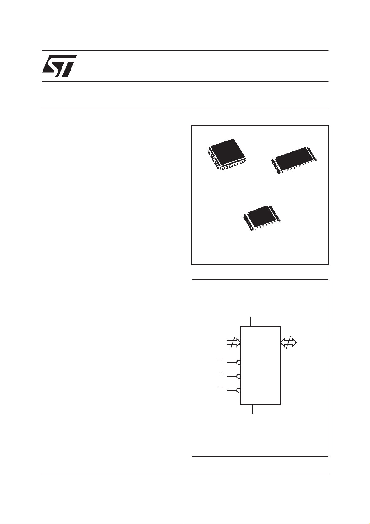
M29W040B
4 Mbit (512Kb x8, Uniform Block)
PLCC32 (K)
TSOP32 (NZ)
8 x 14mm
Figure 1. Logic Diagram
V
CC
19
A0-A18
TSOP32 (N)
8 x 20mm
8
DQ0-DQ7
W
M29W040B
E
G
V
SS
AI02953
1/20March 2000
Page 2
M29W040B
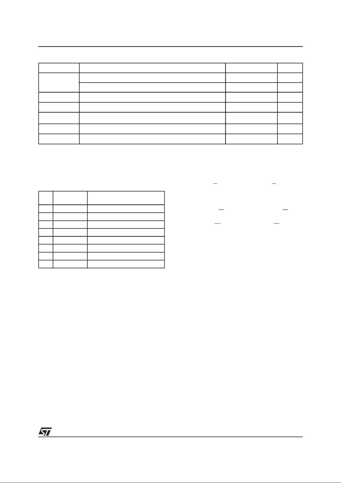
Figure 2. PLCC Connections
A16
A7
A6
A5
A4
A3
A2
A1
A0
DQ0
A12
9
DQ1
A18
A15
1
32
M29W040B
17
SS
V
DQ2
DQ3
V
DQ4
CC
W
DQ5
A17
25
DQ6
A14
A13
A8
A9
A11
G
A10
E
DQ7
AI02951
Figure 3. TSOP Connections
A11 G
A9
A8
A13
A14
A17
V
CC
A18
A16
A15
A12
A7
A6
A5
A4 A3
1
W
8
M29W040B
9
16 17
32
25
24
AI02952
A10
E
DQ7
DQ6
DQ5
DQ4
DQ3
V
SS
DQ2
DQ1
DQ0
A0
A1
A2
Table 1. Signal Names
A0-A18 Address Inputs
DQ0-DQ7 Data Inputs/Outputs
E Chip Enable
G Output Enable
W Write Enable
V
CC
V
SS
Supply Voltage
Ground
SUMMARY DESCRIPTION
The M29W040B is a 4 Mbit (512Kb x8) non-volatile memory that can be read, erased and reprogrammed. These operations can be performed
using a single lowvoltage (2.7 to 3.6V) supply. On
power-up the memory defaults to its Read mode
where itcan be read in the sameway as aROM or
EPROM. The M29W040B is fully backward compatible with theM29W040.
The memory is divided into blocks that can be
erased independently so it is possible to preserve
valid data whileold data is erased. Each block can
be protected independently to prevent accidental
Program or Erase commands from modifying the
memory. Program and Erase commands are written to the Command Interface of the memory. An
on-chip Program/Erase Controller simplifies the
process of programming orerasing the memoryby
taking care of all ofthe special operations that are
required to update thememory contents. The end
of a program or erase operation can be detected
and any error conditions identified. The command
set required to control the memory is consistent
with JEDEC standards.
Chip Enable, Output Enable and Write Enable signals control the bus operation of the memory.
They allow simple connection to most microprocessors, often without additional logic.
The memory is offered in TSOP32 (8 x 20mm),
TSOP32 (8 x 14mm) and PLCC32 packages and
it is supplied with all the bits erased (set to ‘1’).
2/20
Page 3
M29W040B
Table 2. Absolute Maximum Ratings
Symbol Parameter Value Unit
T
A
T
BIAS
T
STG
(2)
V
IO
V
CC
V
ID
Note: 1. Except for the rating ”Operating Temperature Range”, stresses above those listed in the Table ”Absolute Maximum Ratings” may
cause permanent damage to the device. These are stress ratings only and operation of the device at these or anyother conditions
above those indicated in the Operating sections of this specification is not implied. Exposure to Absolute Maximum Rating conditions for extended periods may affect device reliability. Refer also to theSTMicroelectronics SURE Program andotherrelevant quality documents.
2. Minimum Voltage may undershoot to –2V during transition and for less than 20ns during transitions.
Ambient Operating Temperature (Temperature Range Option 1) 0 to 70 °C
Ambient Operating Temperature (Temperature Range Option 6) –40 to 85 °C
Temperature Under Bias –50 to 125 °C
Storage Temperature –65 to 150 °C
Input or Output Voltage –0.6 to 4 V
Supply Voltage –0.6 to 4 V
Identification Voltage –0.6 to 13.5 V
Table 3. Uniform Block Addresses, M29W040B
#
7 64 70000h-7FFFFh
6 64 60000h-6FFFFh
5 64 50000h-5FFFFh
4 64 40000h-4FFFFh
3 64 30000h-3FFFFh
2 64 20000h-2FFFFh
1 64 10000h-1FFFFh
0 64 00000h-0FFFFh
Size
(Kbytes)
Address Range
(1)
Chip Enable (E). The Chip Enable, E, activates
the memory, allowingBus Read and BusWrite operations to be performed. When Chip Enable is
High, VIH, all other pins are ignored.
Output Enable (G). The Output Enable, G, controls the Bus Read operation of the memory.
Write Enable (W). The Write Enable, W, controls
the Bus Write operation of the memory’s Command Interface.
VCCSupply Voltage. The VCCSupply Voltage
supplies the power for all operations (Read, Program, Eraseetc.).
The Command Interface is disabledwhen the V
CC
Supply Voltage is less than the Lockout Voltage,
V
. Thisprevents Bus Write operationsfrom ac-
SIGNAL DESCRIPTIONS
See Figure 1, Logic Diagram, and Table 1, Signal
Names, forabriefoverview ofthesignalsconnected to this device.
Address Inputs (A0-A18). The Address Inputs
select thecells in the memoryarray to access during BusRead operations. During Bus Write operations they control the commands sent to the
Command Interface of the internal state machine.
Data Inputs/Outputs (DQ0-DQ7). The Data Inputs/Outputs outputthe data storedatthe selected
address during aBus Readoperation. During Bus
Write operations they represent the commands
LKO
cidentally damaging the data during power-up,
power-down and power surges. If the Program/
Erase Controller is programming or erasing during
this time then the operationaborts and the memory contents being altered will be invalid.
A 0.1µF capacitor should be connected between
the VCCSupply Voltage pin and the VSSGround
pin to decouple the current surges from the power
supply. ThePCB track widthsmust be sufficientto
carry the currents required during program and
erase operations,I
CC3
.
VSSGround. The VSSGroundis the reference for
all voltage measurements.
sent tothe CommandInterfaceof the internal state
machine.
3/20
Page 4
M29W040B
BUS OPERATIONS
There are fivestandard bus operations thatcontrol
the device. These are Bus Read, Bus Write, Output Disable,Standby andAutomatic Standby. See
Table 4,Bus Operations,for asummary. Typically
glitches of less than 5ns on Chip Enable or Write
Enable are ignored by the memory and do not affect busoperations.
Bus Read. Bus Read operations read from the
memory cells, or specific registers in the Command Interface. A valid Bus Read operation involves settingthe desired address on theAddress
Inputs, applying a Low signal, VIL, to Chip Enable
and Output Enable and keeping Write Enable
High, VIH. The Data Inputs/Outputs will output the
value, see the Figure 8, Read Mode AC Waveforms, and Table 11, Read AC Characteristics, for
details of when the output becomes valid.
Bus Write. Bus Write operations write to the
Command Interface. A valid Bus Write operation
begins by setting the desired address on the Address Inputs. The Address Inputs are latched by
the CommandInterface on thefalling edge of Chip
Enable or Write Enable, whichever occurs last.
The Data Inputs/Outputs are latched by the Command Interface on the rising edge of Chip Enable
or WriteEnable, whicheveroccursfirst.Output Enable must remain High, VIH, during the whole Bus
Write operation. See Figures 9 and 10 Write AC
Waveforms, and Tables 12 and 13, Write AC
Characteristics, for details of the timing requirements.
Output Disable. The Data Inputs/Outputs are in
the high impedance state when Output Enable is
High, VIH.
Standby. When Chip Enable is High, VIH, the
memory enters Standby mode and the Data Inputs/Outputs pins are placed in the high-impedance state. To reduce the Supply Current to the
Standby Supply Current, I
, ChipEnable should
CC2
be held withinVCC± 0.2V.For the Standby current
level see Table 10, DC Characteristics.
During program or erase operations the memory
will continue to use the Program/Erase Supply
Current, I
, forProgramor Erase operationsun-
CC3
til the operation completes.
Automatic Standby. If CMOSlevels (VCC± 0.2V)
are used to drive the bus andthe bus is inactive for
150ns or more the memory enters Automatic
Standby where the internal Supply Current is reduced to the Standby Supply Current, I
CC2
. The
Data Inputs/Outputs will still output data if a Bus
Read operation is in progress.
Special Bus Operations
Additional bus operations can be performed to
read the Electronic Signature and also to apply
and remove Block Protection. These bus operations are intended for use by programming equipment and are not usually used in applications.
They require VIDto be applied to some pins.
Electronic Signature. The memory has two
codes, the manufacturer code and the device
code, that can be read to identify the memory.
These codes can be read by applying the signals
listed in Table 4, Bus Operations.
Block Protection and BlocksUnprotection. Each
block can be separately protected against accidental Program or Erase.Protected blocks canbe
unprotected to allow data to be changed. Block
Protection and Blocks Unprotection operations
must only be performed on programming equipment. For further information refer to Application
Note AN1122, Applying Protection and Unprotection to M29 Series Flash.
Table 4. Bus Operations
Operation E G W Address Inputs
Bus Read
Bus Write V
Output Disable
Standby V
Read Manufacturer
Code
Read Device Code
Note: X = VILor VIH.
4/20
V
IL
IL
XV
IH
V
IL
V
IL
V
IL
V
IH
IH
XXX Hi-Z
V
IL
V
IL
Data
Inputs/Outpu ts
V
V
V
V
V
Cell Address Data Output
IH
Command Address Data Input
IL
XHi-Z
IH
A0 = VIL,A1=VIL,A9=VID,
IH
Others V
A0 = VIL,A1=VIL,A9=VID,
IH
Others V
or V
IL
or V
IL
IH
IH
20h
E3h
Page 5

M29W040B
COMMAND INTERFACE
All Bus Write operations to the memory are interpreted by the Command Interface. Commands
consist of one or more sequential Bus Write operations. Failureto observe a valid sequence of Bus
Write operations will result in the memory returning to Readmode.The long command sequences
are imposed to maximize data security.
The commands are summarized in Table 5, Commands. Refer to Table 5 in conjunction with the
text descriptions below.
Read/Reset Command. The Read/Reset command returnsthe memory toits Read mode where
it behaves like a ROM or EPROM. It also resets
the errors in the Status Register. Either one or
three Bus Write operations can be used to issue
the Read/Reset command.
If the Read/Reset command is issued during a
Block Eraseoperation or followinga Programming
or Eraseerror then thememory will take upto 10µs
to abort. Duringthe abort period no valid data can
be read from the memory. Issuing a Read/Reset
command during a Block Erase operation will
leave invalid datain the memory.
Auto Select Command. The Auto Select command is used to read the Manufacturer Code, the
Device Code and the Block Protection Status.
Three consecutive Bus Write operations are required to issue the Auto Select command. Once
the Auto Select command is issued the memory
remains in Auto Select mode until another command is issued.
From the Auto Select mode the Manufacturer
Code can be read using a Bus Read operation
with A0 = VILand A1 = VIL. The other address bits
may be set to either VILor VIH. The Manufacturer
Code for STMicroelectronics is 20h.
The Device Code can be read using a Bus Read
operation with A0 = VIHand A1 = VIL. The other
address bits may be set to either VILor VIH.The
Device Code for the M29W040B is E3h.
The Block Protection Status of each block can be
read using a Bus Read operation with A0 = VIL,
A1 = VIH, and A16, A17andA18specifying the address of the block. The other address bits may be
set to either VILor VIH. If the addressed block is
protected then 01h is output on the Data Inputs/
Outputs, otherwise 00h is output.
Program Command. The Program command
can be usedto program a value to one addressin
the memory array at a time. The command requires fourBus Writeoperations,the finalwriteoperation latchestheaddressand data inthe internal
state machine and starts the Program/Erase Controller.
If the address falls in a protected block then the
Program command is ignored, the data remains
unchanged. The Status Registerisnever read and
no errorcondition is given.
During the program operation the memory will ignore all commands. It is not possible to issue any
command to abort or pause the operation. Typical
program timesare given in Table 6.Bus Read operations during the program operation will output
the Status Register on the Data Inputs/Outputs.
See the section on the Status Register for more
details.
After the program operation has completed the
memory will return to the Read mode, unless an
error has occurred. When an error occurs the
memory will continue to output the Status Register. A Read/Reset command must be issued to reset the error condition and return to Read mode.
Note thatthe Programcommand cannotchange a
bit set at ‘0’ back to ‘1’. One of the Erase Commands must beused to setall the bits in a block or
in the wholememory from ‘0’ to ‘1’.
Unlock Bypass Command. The Unlock Bypass
command is used in conjunction with the Unlock
Bypass Program commandto programthe memory. When the access time to the device is long (as
with some EPROM programmers) considerable
time saving can be made by using these commands. Three Bus Write operations are required
to issue the Unlock Bypass command.
Once the Unlock Bypass command has been issued the memory will only accept the Unlock Bypass Program command and the Unlock Bypass
Reset command. The memorycan be read as if in
Read mode.
Unlock Bypass Program Command. The Un-
lock Bypass Program command can be used to
program one address in memory at a time. The
command requires two Bus Write operations, the
final write operation latches the address and data
in the internal state machine and starts the Program/Erase Controller.
The Program operation using the Unlock Bypass
Program command behaves identically tothe Program operation using the Program command. A
protected block cannot be programmed; the operation cannot be aborted and theStatusRegister is
read. Errors must be reset using the Read/Reset
command, which leaves the device in Unlock Bypass Mode. See the Programcommand for details
on thebehavior.
Unlock Bypass Reset Command. The Unlock
Bypass Reset command can be used to return to
Read/Reset mode from Unlock Bypass Mode.
TwoBus Write operations are requiredtoissue the
Unlock Bypass Reset command.
5/20
Page 6
M29W040B
Table 5. Commands
Bus Write Operations
Command
Read/Reset
Auto Select 3 555 AA 2AA 55 555 90
Program 4 555 AA 2AA 55 555 A0 PA PD
Unlock Bypass 3 555 AA 2AA 55 555 20
Unlock Bypass
Program
Unlock Bypass Reset 2 X 90 X 00
Chip Erase 6 555 AA 2AA 55 555 80 555 AA 2AA 55 555 10
Block Erase 6+ 555 AA 2AA 55 555 80 555 AA 2AA 55 BA 30
Erase Suspend 1 X B0
Erase Resume 1 X 30
Note: X Don’t Care, PA Program Address, PD Program Data, BA Any address in the Block.
All values in the table are in hexadecimal.
The Command Interface only uses address bits A0-A10 to verify the commands, the upper address bits are Don’t Care.
Read/Reset. After a Read/Reset command, read the memory as normal until another command is issued.
Auto Select. After anAuto Select command, read Manufacturer ID, Device ID or Block Protection Status.
Program, Unlock Bypass Program, Chip Erase, Block Erase. After these commands read the Status Register until the Program/Erase
Controller completes and the memory returns to Read Mode. Add additional Blocks during Block Erase Command with additional BusWrite
Operations until the Timeout Bit is set.
Unlock Bypass. After the Unlock Bypass command issue Unlock Bypass Program or Unlock Bypass Reset commands.
Unlock Bypass Reset. After the Unlock Bypass Reset command read the memory as normal until another command is issued.
Erase Suspend. After the Erase Suspend command readnon-erasing memory blocksas normal, issue AutoSelect and Program commands
on non-erasing blocks as normal.
Erase Resume. After the Erase Resume command the suspended Erase operation resumes, read the Status Register until the Program/
Erase Controller completes and the memory returns toRead Mode.
1X F0
3 555 AA 2AA 55 X F0
2X A0PAPD
1st 2nd 3rd 4th 5th 6th
Length
Addr Data Addr Data Addr Data Addr Data Addr Data Addr Data
Chip Erase Command. The Chip Erase com-
mand canbeusedto erase the entirechip. Six Bus
Write operations are required to issue the Chip
Erase Command and start the Program/Erase
Controller.
If any blocksare protected then these are ignored
and all the other blocks are erased. If all of the
blocks are protected the ChipErase operation appears tostart butwillterminate within about 100µs,
leaving the data unchanged. No error condition is
given when protected blocks are ignored.
During the erase operationthe memory will ignore
all commands. It is not possible to issue any command to abort the operation. Typical chip erase
6/20
times are given in Table 6. All Bus Read operations during the Chip Erase operation will output
the Status Register on the Data Inputs/Outputs.
See the section on the Status Register for more
details.
After the Chip Erase operation has completed the
memory will return to the Read Mode, unless an
error has occurred. When an error occurs the
memory will continue to output the Status Register. A Read/Reset command must be issued to reset the error condition and return to Read Mode.
TheChip Erase Commandsetsallof the bitsinunprotected blocks of the memory to ‘1’. All previous
data is lost.
Page 7

M29W040B
Block Erase Command. The Block Erase com-
mand can be used to erase a list of one or more
blocks. Six Bus Write operations are required to
select the first block in the list. Each additional
block in the list can be selected by repeating the
sixth Bus Write operation using the address of the
additional block. The Block Erase operation starts
the Program/Erase Controller about 50µs after the
last BusWrite operation. Oncethe Program/Erase
Controller starts it is not possible to select any
more blocks.Each additionalblock must therefore
be selectedwithin50µs of the last block.The 50µs
timer restartswhenan additional block isselected.
The Status Register can be read after the sixth
Bus Write operation. See the Status Register for
details on how to identify if the Program/Erase
Controller has started the Block Erase operation.
If anyselectedblocks are protected thenthese are
ignored and all the other selected blocks are
erased. If all of the selected blocks are protected
the Block Eraseoperation appears tostart but will
terminate withinabout 100µs, leaving thedata un-
changed. Noerrorcondition isgiven whenprotected blocks are ignored.
During the Block Erase operation the memory will
ignore all commands except the Erase Suspend
and Read/Reset commands. Typical block erase
times are given in Table 6. All Bus Read operations during the Block Erase operation will output
the Status Register on the Data Inputs/Outputs.
See the section on the Status Register for more
details.
After theBlock Erase operationhas completed the
memory will return to the Read Mode, unless an
error has occurred. When an error occurs the
memory will continue to output the Status Regis-
ter. A Read/Reset command must be issued to reset the error condition and return to Read mode.
The Block Erase Command sets all of the bits in
the unprotectedselected blocks to ‘1’. All previous
data in the selected blocks is lost.
Erase Suspend Command. The Erase Suspend
Command may be used totemporarily suspend a
Block Erase operation and return the memory to
Read mode. The command requires one Bus
Write operation.
The Program/Erase Controller will suspend within
15µs of the Erase Suspend Command being issued. Once the Program/Erase Controller has
stopped thememory will be set toRead modeand
the Erase willbe suspended. IftheErase Suspend
command is issued during the period when the
memory is waiting for an additional block (before
the Program/Erase Controller starts) then the
Erase is suspendedimmediately and will start immediately when the Erase Resume Command is
issued. It will not be possible to select any further
blocks for erasure after the EraseResume.
During Erase Suspend it is possible to Read and
Program cells in blocks that are not being erased;
both Read and Program operations behave as
normal on these blocks. Reading from blocks that
are being erased willoutput the Status Register. It
is also possible toenter theAuto Select mode: the
memorywill behaveas in theAuto Select mode on
all blocks untila Read/Reset commandreturnsthe
memory to Erase Suspend mode.
Erase Resume Command. The Erase Resume
command must be used to restart the Program/
Erase Controller from Erase Suspend. An erase
can be suspended and resumed more than once.
Table 6. Program, Erase Times and Program, Erase EnduranceCycles
(TA= 0 to 70°C or –40 to 85°C)
Parameter Min
Chip Erase (All bits in the memory set to‘0’) 2.5 2.5 sec
Chip Erase 6 6 35 sec
Block Erase (64 Kbytes) 0.8 0.8 6 sec
Program 10 10 200 µs
Chip Program 5.5 5.5 30 sec
Program/Erase Cycles (per Block) 100,000 cycles
Note: 1. TA=25°C, VCC= 3.3V.
Typ
(1)
Typical after
100k W/E Cycles
(1)
Max Unit
7/20
Page 8

M29W040B
STATUS REGISTER
Bus Read operations from any address always
read the Status Register during Program and
Erase operations.It is also read during EraseSuspend whenanaddress within ablock beingerased
is accessed.
The bits in the Status Register are summarized in
Table 7, Status RegisterBits.
Data Polling Bit (DQ7). The Data Polling Bit can
be used to identify whether the Program/Erase
Controller has successfully completed its operation or if it has responded to an Erase Suspend.
The Data Polling Bit is output on DQ7 when the
Status Register is read.
During Program operations the Data Polling Bit
outputs the complement of the bit being programmed to DQ7. After successful completion of
the Program operation the memory returns to
Read modeand Bus Read operationsfrom the address just programmed output DQ7, not its complement.
During Erase operations the Data Polling Bit outputs ‘0’, the complement of the erased state of
DQ7. Aftersuccessful completion of theErase operation the memory returns to Read mode.
In Erase Suspend mode the Data Polling Bit will
output a ‘1’ during a Bus Read operation within a
block being erased. The Data Polling Bit will
change froma ‘0’to a‘1’ whenthe Program/Erase
Controller has suspendedthe Erase operation.
Figure 3, Data Polling Flowchart, gives an example of how to use theData Polling Bit. A Valid Address is the address being programmed or an
address within the block being erased.
Toggle Bit (DQ6). The Toggle Bit can be used to
identify whethertheProgram/Erase Controllerhas
successfully completedits operation or if ithas responded to an Erase Suspend. The Toggle Bit is
output on DQ6 when the Status Register is read.
During Program and Erase operations the Toggle
Bit changes from ‘0’ to ‘1’ to ‘0’, etc., with successive Bus Read operations at any address. After
successful completionof the operation the memory returns to Read mode.
During Erase Suspend mode the Toggle Bit will
output when addressinga cellwithin ablock being
erased. TheToggle Bit will stop toggling when the
Program/Erase Controller has suspended the
Erase operation.
Figure 4, Data Toggle Flowchart, gives an example of howto use the Data Toggle Bit.
Error Bit (DQ5). The Error Bit can be used to
identify errors detected by the Program/Erase
Controller. The Error Bit is set to ‘1’ when a Program, BlockErase orChip Erase operation fails to
write the correct data to the memory. If the Error
Bit is set a Read/Reset command must be issued
before other commands are issued. The Error bit
is output onDQ5when the Status Registerisread.
Note thatthe Programcommand cannotchange a
bit set at ‘0’backto ‘1’ andattemptingto do so may
or may not set DQ5 at ‘1’. In bothcases, a successive Bus Readoperation will showthe bit isstill ‘0’.
One of the Erase commands must be used to set
all the bits in a blockor in the whole memoryfrom
‘0’ to ‘1’.
Table 7. Status Register Bits
Operation Address DQ7 DQ6 DQ5 DQ3 DQ2
Program Any Address DQ7 Toggle 0 – –
Program During Erase
Suspend
Program Error Any Address DQ7 Toggle 1 – –
Chip Erase Any Address 0 Toggle 0 1 Toggle
Block Erase before
timeout
Block Erase
Erase Suspend
Erase Error
Note: Unspecified data bits should be ignored.
8/20
Any Address DQ7 Toggle 0 – –
Erasing Block 0 Toggle 0 0 Toggle
Non-Erasing Block 0 Toggle 0 0 No Toggle
Erasing Block 0 Toggle 0 1 Toggle
Non-Erasing Block 0 Toggle 0 1 No Toggle
Erasing Block 1 No Toggle 0 – Toggle
Non-Erasing Block Data read as normal
Good Block Address 0 Toggle 1 1 No Toggle
Faulty Block Address 0 Toggle 1 1 Toggle
Page 9

M29W040B
Figure 4. Data Polling Flowchart
START
READ DQ5&
at VALID ADDRESS
NO
READ
at VALID ADDRESS
DQ7
DQ7
DATA
DQ5
DQ7
DATA
FAIL PASS
=
=1
=
NO
YES
DQ7
NO
YES
YES
AI03598
Figure 5. Data Toggle Flowchart
START
READ
DQ5 & DQ6
READ DQ6
DQ6
=
TOGGLE
NO
DQ5
=1
READ
TWICE
DQ6
=
TOGGLE
FAIL PASS
YES
YES
DQ6
YES
NO
NO
AI01370B
Erase Timer Bit(DQ3). The Erase Timer Bit can
be used to identify the start of Program/Erase
Controller operation during a Block Erase command. Once the Program/Erase Controller starts
erasing theErase Timer Bit is set to ‘1’. Beforethe
Program/Erase Controller starts the Erase Timer
Bit is set to ‘0’ and additional blocks to be erased
may be written to the Command Interface. The
Erase Timer Bit is outputon DQ3 when the Status
Register is read.
Alternative Toggle Bit (DQ2). The Alternative
Toggle Bit can be used to monitor the Program/
Erase controller during Erase operations. The Alternative Toggle Bit is output on DQ2 when the
Status Register is read.
During Chip Erase andBlock Eraseoperations the
Toggle Bit changes from ‘0’ to ‘1’ to ‘0’, etc., with
successive Bus Read operations from addresses
within the blocks beingerased. Oncetheoperation
completes the memory returns to Read mode.
During Erase Suspend the Alternative Toggle Bit
changes from ‘0’ to ‘1’ to ‘0’, etc. with successive
Bus Read operations from addresses within the
blocks being erased. Bus Read operations to addresses within blocks not being erased will output
the memory cell data as if in Read mode.
After an Erase operationthat causes the Error Bit
to be set the Alternative Toggle Bit can be used to
identify whichblock or blocks have caused the error. TheAlternative Toggle Bit changes from ‘0’ to
‘1’ to ‘0’, etc. with successive Bus Read Operations from addresses within blocks that have not
erased correctly. The Alternative Toggle Bit does
not changeif the addressed block has erased correctly.
9/20
Page 10

M29W040B
Table 8. AC Measurement Conditions
Parameter
V
Supply Voltage
CC
M29W040B
55 70 90 / 120
3.0 to 3.6V 2.7 to3.6V 2.7 to 3.6V
Load Capacitance (C
) 30pF 30pF 100pF
L
Input Rise and Fall Times ≤ 10ns ≤ 10ns ≤ 10ns
Input Pulse Voltages 0 to 3V 0 to3V 0 to 3V
Input and Output Timing Ref.Voltages 1.5V 1.5V 1.5V
Figure 6. AC Testing Input Output Waveform
3V
1.5V
0V
AI01417
Figure 7. AC TestingLoad Circuit
0.8V
1N914
3.3kΩ
DEVICE
UNDER
TEST
CL= 30pF or100pF
OUT
CLincludes JIG capacitance
Table 9. Capacitance
(TA=25°C, f = 1 MHz)
Symbol Parameter Test Condition Min Max Unit
V
V
IN
OUT
=0V
=0V
6pF
12 pF
C
IN
C
OUT
Note: Sampled only, not 100% tested.
Input Capacitance
Output Capacitance
10/20
AI02762
Page 11

Table 10. DC Characteristics
(TA= 0 to 70°C or –40 to 85°C)
Symbol Parameter Test Condition Min
I
Input Leakage Current
LI
I
I
CC1
I
CC2
I
CC3
V
V
V
V
V
V
LKO
Note: 1. Sampled only, not 100% tested.
Output Leakage Current 0V ≤ V
LO
Supply Current (Read)
Supply Current (Standby)
(1)
Supply Current (Program/Erase)
Input Low Voltage –0.5 0.8 V
IL
Input High Voltage
IH
Output Low Voltage
OL
Output High Voltage IOH= –100µAV
OH
Identification Voltage 11.5 12.5 V
ID
I
Identification Current
ID
Program/Erase Lockout Supply
(1)
Voltage
=25°C, VCC= 3.3V.
2. T
A
0V ≤ V
E=V
,G=VIH, f = 6MHz
IL
E=V
Program/Erase
Controller active
I
OL
A9 = V
≤ V
IN
≤ V
OUT
± 0.2V
CC
= 1.8mA
ID
CC
CC
0.7V
CC
M29W040B
(2)
Typ.
410mA
30 100 µA
CC
– 0.4 V
1.8 2.3 V
Max Unit
±1 µA
±1 µA
20 mA
VCC+ 0.3
0.45 V
100 µA
V
11/20
Page 12

M29W040B
Table 11. Read AC Characteristics
(TA= 0 to 70°C or –40 to 85°C)
Symbol Alt Parameter Test Condition
E=V
,
t
AVAV
t
AVQV
t
ELQX
(1)
t
t
ACC
t
Address Validto Next Address Valid
RC
Address Validto Output Valid
Chip Enable Low to Output
LZ
Transition
G=V
E=V
G=V
G=V
IL
IL
,
IL
IL
IL
M29W040B
Unit
55 70 90 / 120
Min 55 70 90 ns
Max 55 70 90 ns
Min 0 0 0 ns
t
Chip Enable Low to Output Valid
t
OLZ
t
t
t
t
CE
Output Enable Low to Output
Transition
Output Enable Low to Output Valid
OE
Chip Enable High to Output Hi-Z
HZ
Output Enable High to Output Hi-Z
DF
Chip Enable, Output Enableor
Address Transitionto Output
OH
Transition
t
ELQV
(1)
t
GLQX
t
GLQV
(1)
t
EHQZ
(1)
t
GHQZ
t
EHQX
t
GHQX
t
AXQX
Note: 1. Sampled only, not 100% tested.
Figure 8. Read Mode AC Waveforms
A0-A18
tAVQV tAXQX
E
tAVAV
VALID
G=V
E=V
E=V
G=V
E=V
Max 55 70 90 ns
IL
Min 0 0 0 ns
IL
Max 30 30 35 ns
IL
Max 20 25 30 ns
IL
Max 20 25 30 ns
IL
Min 0 0 0 ns
12/20
G
DQ0-DQ7
tELQV tEHQX
tELQX tEHQZ
tGLQX tGHQX
tGLQV
tGHQZ
VALID
AI02903
Page 13

Table 12. Write ACCharacteristics, Write Enable Controlled
(TA= 0 to 70°C or –40 to 85°C)
Symbol Alt Parameter
t
AVAV
t
ELWL
t
WLWH
t
DVWH
t
WHDX
t
WHEH
t
WHWL
t
AVWL
t
WLAX
t
GHWL
t
WHGL
t
VCHEL
t
WC
t
t
WP
t
t
t
t
WPH
t
t
t
OEH
t
VCS
Address Valid to Next Address Valid Min 55 70 90 ns
Chip Enable Low to Write Enable Low Min 0 0 0 ns
CS
Write Enable Lowto Write Enable High Min 40 45 45 ns
Input Validto Write Enable High Min 25 30 45 ns
DS
Write Enable High to Input Transition Min 0 0 0 ns
DH
Write Enable High to Chip Enable High Min 0 0 0 ns
CH
Write Enable High to Write Enable Low Min 30 30 30 ns
Address Valid to Write Enable Low Min 0 0 0 ns
AS
Write Enable Lowto Address Transition Min 40 45 45 ns
AH
Output Enable High to Write Enable Low Min 0 0 0 ns
Write Enable High to Output Enable Low Min 0 0 0 ns
VCCHigh to Chip Enable Low
M29W040B
M29W040B
Unit
55 70 90 / 120
Min 50 50 50 µs
Figure 9. Write AC Waveforms, Write Enable Controlled
tAVAV
A0-A18
E
G
W
DQ0-DQ7
V
CC
tAVWL
tELWL
tVCHEL
VALID
tWLWHtGHWL
tDVWH
tWLAX
tWHEH
tWHGL
tWHWL
tWHDX
VALID
AI02908
13/20
Page 14

M29W040B
Table 13. Write ACCharacteristics, Chip Enable Controlled
(TA= 0 to 70°C or –40 to 85°C)
Symbol Alt Parameter
t
AVAV
t
WLEL
t
ELEH
t
DVEH
t
EHDX
t
EHWH
t
EHEL
t
AVEL
t
ELAX
t
GHEL
t
EHGL
t
VCHWL
t
WC
t
WS
t
CP
t
DS
t
DH
t
WH
t
CPH
t
AS
t
AH
t
OEH
t
VCS
Address Valid to Next Address Valid Min 55 70 90 ns
Write Enable Lowto Chip Enable Low Min 0 0 0 ns
Chip Enable Low to Chip Enable High Min 40 45 45 ns
Input Validto Chip Enable High Min 25 30 45 ns
Chip Enable High to Input Transition Min 0 0 0 ns
Chip Enable High to Write Enable High Min 0 0 0 ns
Chip Enable High to Chip Enable Low Min 30 30 30 ns
Address Valid to Chip Enable Low Min 0 0 0 ns
Chip Enable Low to Address Transition Min 40 45 45 ns
Output Enable High Chip Enable Low Min 0 0 0 ns
Chip Enable High to Output Enable Low Min 0 0 0 ns
VCCHigh to Write Enable Low
M29W040B Unit
55 70 90 / 120
Min 50 50 50 µs
Figure 10. Write AC Waveforms, Chip Enable Controlled
tAVAV
A0-A18
W
G
E
DQ0-DQ7
V
CC
tAVEL
tWLEL
tVCHWL
VALID
tELEHtGHEL
tDVEH
tELAX
tEHWH
tEHGL
tEHEL
tEHDX
VALID
AI02909
14/20
Page 15

Table 14. Ordering Information Scheme
Example: M29W040B 55 N 1 T
Device Type
M29
Operating Voltage
W=V
Device Function
040B = 4 Mbit (512Kb x8), Uniform Block
Speed
55 = 55 ns
70 = 70 ns
90 = 90 ns
120 = 120 ns
Package
K = PLCC32
N = TSOP32: 8 x 20 mm
NZ = TSOP32: 8 x 14 mm
= 2.7 to 3.6V
CC
M29W040B
Temperature Range
1=0to70°C
6=–40to85°C
Option
T = Tape & Reel Packing
Note: The last two characters of the ordering code may be replaced by a letter code for preprogrammed
parts, otherwise devicesare shipped fromthe factory with the memory content bits erased to ‘1’.
For a list of available options (Speed, Package, etc...) or for further information on any aspect of this device, please contactthe ST Sales Office nearest to you.
15/20
Page 16

M29W040B
Table 15. Revision History
Date Revision Details
July 1999 First Issue
Typ.specification added (Table 10)
I
09/21/99
03/09/00
CC1
Typ.specification added (Table 10)
I
CC2
Document type: from Preliminary Data to Data Sheet
Status Register bit DQ5 clarification
Data Polling Flowchart diagram change (Figure 4)
Data ToggleFlowchart diagram change (Figure 5)
16/20
Page 17

M29W040B
Table 16. PLCC32 - 32lead Plastic Leaded Chip Carrier, rectangular, Package Mechanical Data
Symbol
A 2.54 3.56 0.1000 0.1402
A1 1.52 2.41 0.0598 0.0949
A2 0.38 0.0150
B 0.33 0.53 0.0130 0.0209
B1 0.66 0.81 0.0260 0.0319
D 12.32 12.57 0.4850 0.4949
D1 11.35 11.56 0.4469 0.4551
D2 9.91 10.92 0.3902 0.4299
E 14.86 15.11 0.5850 0.5949
E1 13.89 14.10 0.5469 0.5551
E2 12.45 13.46 0.4902 0.5299
e 1.27 – – 0.0500 – –
F 0.00 0.25 0.0000 0.0098
R 0.89 – – 0.0350 – –
N32 32
Nd 7 7
Ne 9 9
CP 0.10 0.0039
Typ Min Max Typ Min Max
mm inches
Figure 11. PLCC32 - 32 lead Plastic Leaded Chip Carrier, rectangular, Package Outline
D
D1
1N
Ne E1 E
F
D2/E2
A2
B
0.51 (.020)
1.14 (.045)
PLCC
Drawing is notto scale.
Nd
R
CP
A
A1
B1
e
17/20
Page 18

M29W040B
Table 17. TSOP32 - 32lead Plastic Thin Small Outline, 8 x 20mm, Package Mechanical Data
Symbol
Typ Min Max Typ Min Max
A 1.20 0.0472
A1 0.05 0.15 0.0020 0.0059
A2 0.95 1.05 0.0374 0.0413
B 0.15 0.27 0.0059 0.0106
C 0.10 0.21 0.0039 0.0083
D 19.80 20.20 0.7795 0.7953
D1 18.30 18.50 0.7205 0.7283
E 7.90 8.10 0.3110 0.3189
e 0.50 – – 0.0197 – –
L 0.50 0.70 0.0197 0.0276
α 0° 5° 0° 5°
N32 32
CP 0.10 0.0039
mm inches
Figure 12. TSOP32 - 32 lead Plastic Thin Small Outline, 8 x 20mm, Package Outline
A2
1N
e
E
B
N/2
D1
D
DIE
A
CP
C
TSOP-a
Drawing is notto scale.
LA1 α
18/20
Page 19

M29W040B
Table 18. TSOP32 - 32 lead Plastic Thin Small Outline, 8 x 14mm, Package Mechanical Data
Symbol
A 1.20 0.0472
A1 0.05 0.15 0.0020 0.0059
A2 0.95 1.05 0.0374 0.0413
B 0.17 0.27 0.0067 0.0106
C 0.10 0.21 0.0039 0.0083
D 13.80 14.20 0.5433 0.5591
D1 12.30 12.50 0.4843 0.4921
E 7.90 8.10 0.3110 0.3189
e 0.50 – – 0.0197 – –
L 0.50 0.70 0.0197 0.0276
α 0° 5° 0° 5°
N32 32
CP 0.10 0.0039
Typ Min Max Typ Min Max
mm inches
Figure 13. TSOP32 - 32 lead Plastic Thin Small Outline, 8 x 14mm, Package Outline
A2
1N
e
E
B
N/2
D1
D
DIE
A
CP
C
TSOP-a
Drawing is notto scale.
LA1 α
19/20
Page 20

M29W040B
Information furnished is believed to be accurate and reliable. However, STMicroelectronics assumes no responsibility for the consequences
of use ofsuch information nor for any infringement of patents orother rights of thirdparties whichmay result from itsuse. No license is granted
by implication or otherwise under any patent or patent rights of STMicroelectronics. Specifications mentioned in this publication are subject
to change without notice. This publication supersedes and replaces allinformation previously supplied. STMicroelectronics products are not
authorized for use as critical components in life support devicesor systems without express written approval of STMicroelectronics.
The ST logo is registered trademark of STMicroelectronics
2000 STMicroelectronics - All Rights Reserved
All other names are the property of their respective owners.
Australia - Brazil - China - Finland - France - Germany - Hong Kong - India - Italy - Japan -Malaysia - Malta - Morocco -
Singapore - Spain - Sweden - Switzerland - United Kingdom - U.S.A.
STMicroelectronics GROUP OF COMPANIES
http://www.st.com
20/20
 Loading...