

Page 1
Low Voltage Single Supply Flash Memory
M29W008T and M29W008B are replaced
respectively by the M29W008AT and
M29W008AB
2.7V to 3.6V SUPPLY VOLTAG E for
PROGRAM, ERASE and READ OPERATIONS
FAST A CCES S TIME : 100ns
FAST PROGRAMMING TIME: 10µs typical
PROGRAM/ERASE CONTROLLER (P/E.C.)
– Program Byte-by-Byte
– Status Register bits and Ready/Busy Output
MEMOR Y BLOCKS
– Boot Block (Top or Bottom location)
– Parameter and Main blocks
BLOCK, MULTI-BLOCK and CHIP ERASE
MULTI BLOCK PROTECTION/TEMPORARY
UNPROTECTION MODES
ERASE SUSPEND and RESUME MOD ES
– Read and Program another Block during
Erase Suspend
LOW POWER CONSUMPTION
– Stand-by and Automatic Stand-by
100,000 PROGRAM/ERASE CYCLES per
BLOCK
20 YEARS DA TA RETE NT ION
– Defectivity below 1ppm/year
ELECTRONIC SIGNATURE
– Manufacturer Code: 20h
– Device Code, M29W008T: D2h
– Device Code, M29W008B: DCh
DESCRIPTION
The M29W008 is a non-volatile memory that may
be erased electrically at the block or chip level and
programmed in-system on a Byte-by-Byte basis
using only a single 2.7V to 3.6V V
Program and Erase operations the necessary high
voltages are generated internally. The device can
also be programmed in standard programmers.
The array matrix organisation allows each block to
be erased and reprogrammed without affecting
other blocks. Blocks can be protected against programing and erase on programming equipment,
and temporarily unprotected to make changes in
supply. For
CC
M29W008T
M29W008B
8 Mbit (1Mb x8, Boot Block)
NOT FOR NEW DESIGN
TSOP40 (N)
10 x 20 mm
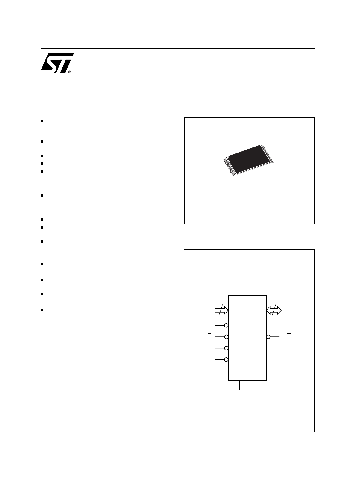
Figure 1. Logic Diagram
V
CC
A0-A19
W
RP
20
E
G
M29W008T
M29W008B
V
SS
8
DQ0-DQ7
RB
AI02189
June 1999 1/30
This is information on a product still in production but not recommended for new designs.
Page 2
M29W008T, M29W008B
Figure 2. TSOP Pin Connections
A16
A15
A14
A13
A12
A11
A9
A8
W
RP
NC
RB
A18
A6
A5
A4
A3
A2
A1
Warning:
NC = Not Connected.
DESCRIPTION
1
M29W008T
10
M29W008B
11
20 21
AI02190
(Cont’d)
40
31
30
A17
V
SS
NC
A19
A10
DQ7
DQ6
DQ5
DQ4
V
CC
V
CC
NC
DQ3
DQ2A7
DQ1
DQ0
G
V
SS
E
A0
the application. Each block can be programmed
and erased over 100,000 cycles.
Instructions for Read/Reset, Auto Select for reading the Electronic Signature or Block Protection
status, Programming, Block and Chip Erase, Erase
Tabl e 1. Signal Names
A0-A19 Address Inputs
DQ0-DQ7 Data Input/Outputs, Command Inputs
E Chip Enable
G Output Enable
W Write Enable
RP Reset / Block Temporary Unprotect
B Ready/Busy Output
R
V
CC
V
SS
Supply Voltage
Ground
Suspend and Resume are written t o the device in
cycles of commands to a Command Interface using
standard microprocessor write timings. The device
is offered in TSOP40 (10 x 20mm) package.
Organisation
The M29W008 is organised as 1Mb x 8. The memory uses the address inputs A0-A19 and the Data
Input/Outputs DQ0-DQ7. Memory control is provided by Chip Enable
Enable
W inputs.
A Reset/Block T emporary Unprotection
E, Output Enable G and Write
RP tri-level
input provides a hardware reset when pulled Low,
and when held High (at V
) temporarily unprotects
ID
blocks previously protected allowing them to be
programed and erased. Erase and Program operations are controlled by an internal Program/Erase
Controller (P/E.C.). Status Register data output on
DQ7 provides a Data Polling signal, and DQ6 and
DQ2 provide Toggle signals to indicate the state of
the P/E.C operations. A Ready/Busy R
B output
indicates the completion of the internal algorithms.
T ab le 2. Absolute Maximum Ratings
Symbol Parameter Value Unit
T
A
T
BIAS
T
STG
(2)
V
IO
V
CC
V
(A9, E, G, RP)
Notes:
1. Except for the rating "Operating Temperature Range", stresses above those listed in the Table "Absolute Maximum Ratings"
may cause permanent damage to the device. These are stress rating s only and operation of the device at these or any other
conditions above those indicated in the Operating sections of this specification is not implied. Exposure to Absolute Maximum
Rating conditions for extended periods may affect device reliability. Refer also to the STMicroelectronics SURE Program and other
relevant quality documents.
2. Minimum Voltage may undershoot to –2V during transition and for less than 20ns.
3. Depends on range.
2/30
Ambient Operating Temperature
Temperature Under Bias –50 to 125
Storage Temperature –65 to 150
Input or Output Voltages –0.6 to 5 V
Supply Voltage –0.6 to 5 V
(2)
A9, E, G, RP Voltage –0.6 to 13.5 V
(1)
(3)
–40 to 85
C
°
C
°
C
°
Page 3

M29W008T, M29W008B
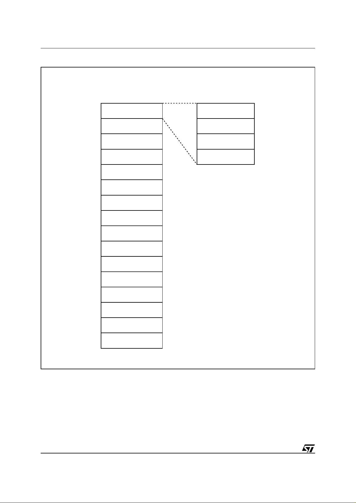
Memory Blocks
The devices feature asymmetrically blocked architecture providing system memory integration. Both
M29W008T and M29W008B devices have an array
of 19 blocks, one Boot Block of 16 Kbytes, two
Parameter Blocks of 8 Kbytes, one Main B lock of
32 Kbytes and fifteen Main Blocks of 64 Kbytes.
The M29W008T has the Boot Block at the top of
the memory address space and the M29W008B
locates the Boot Block starting at the bottom. The
memory maps are showed in Figure 3. E ach block
can be erased separately, any combination of
blocks can be specified for multi-block erase or the
entire chip may be erased. The Erase operations
are managed automatically by the P/E.C. The block
erase operation can be suspended in order to read
from or program to any block not being ersased,
and then resumed.
Block protection provides additional data security.
Each block can be separately protected or unprotected against Program or Erase on programming
equipment. All previously protected blocks can be
temporarily unprotected in the application.
Bus Operations
The following operations can be performed usi ng
the appropriate bus cycles: Read (Array , E lectronic
Signature, Block Protection Status), Write command, Output Disable, Standby, Reset, Block Protection, Unprotection, Protection Verify,
Unprotection Verify and Blo ck Temporary Unprotection. See Tables 4 and 5.
Command Interface
Instructions, made up of commands written in cycles, can be given to the Program/Erase Controller
through a Command Interface (C.I.). For added
data protection, program or erase execution starts
after 4 or 6 cycles. The first, second, fourth and fifth
cycles are used to input Coded cycles to the C.I.
This Coded sequence is the same for all Program/Erase Controller instructions. The ’Command’ itself and its confirmation, when applicable,
are given on the third, four th or sixth cycles. Any
incorrect command or any improper command sequence will reset the device to Read Array mode.
Instructions
Seven instructions are defined to perform Read
Array , Auto Select (to read the Electronic Signature
or Block Protection Status), Program, Block Erase,
Chip Erase, Erase Suspend and Er ase Resume.
The internal P/E.C. automatically handles all timing and verification of the Program and Erase
operations. The Status Register Data Polling, Toggle, Error bits and the R
B output may be read at
any time, during programming or erase, to monitor
the progress of the operation.
Instructions are composed of up to six cycles. The
first two cycles input a Coded sequence to the
Command Interface which is common to all instructions (see Table 8). The third cycle inputs the
instruction set-up command. Subsequent cycles
output the addressed data, Electronic Signature or
Block Protection Status for Read operations. In
order to give additional data protection, the instructions for Program and Block or Chip Erase require
further command inputs. For a P rogram instruction,
the fourth command cycle inputs the address and
data to be programmed. For an Erase instruction
(Block or Chip), the fourth and fifth cycles input a
further Coded sequence before the Erase confirm
command on the sixth cycle. Erasure of a memory
block may be suspended, in order to read data from
another block or to program data in another block,
and then resumed.
When power is first applied or if Vcc falls below
, the command interface is reset to Read
V
LKO
Array.
SIGNAL DESCRIP TIONS
See Figure 1 and T able 1.
Address Inputs (A0-A19)
. The address inputs for
the memory array are latched during a write operation on the falling edge of Chip E nable
Enable
W. When A9 is raised to VID, either a Read
E or Write
Electronic Signature Manufacturer or Dev ice Code,
Block Protection Status or a W rite Block P rotection
or Block Unprotection is enabled depending on t he
combination of levels on A0, A 1, A12 and A 15.
Data Input/Outputs (DQ0-DQ7).
The input is data
to be programmed in the memory arr ay or a command to be written to t he C.I. Both are latched on
the rising edge of Chip Enable
E or Write Enable
W. The output is data from the Memory Array, the
Electronic Signature Manufacturer or Device
codes, the Block Protection Status or the Status
register Data Polling bit DQ7, the Toggle Bits DQ6
and DQ2, the Error bit DQ5 or the Erase Timer bit
DQ3. Outputs are valid when Chip Enable
Output Enable
G are active. The output is high
E and
impedance when the chip is deselected or the
outputs are disabled and when
The Chip Enable input activates
Chip Enable (
E).
RP is at a Low level.
the memory control logic, input buffers, dec oders
and sense amplifiers.
E High deselects the memory
and reduces the power consumption to the standby
E can also be used to control writing to the
level.
command register and to the memory array, while
W remains at a low level. The Chip Enable must be
forced to V
during the Block Unprotection opera-
ID
tion.
3/30
Page 4
M29W008T, M29W008B
Figure 3A. Top Boot Block Memory Map and Block Address Table
TOP BOOT BLOCK
Byte-Wide Byte-Wide
FFFFFh
F0000h
EFFFFh
64K MAIN BLOCK
E0000h
DFFFFh
64K MAIN BLOCK
D0000h
CFFFFh
64K MAIN BLOCK
C0000h
BFFFFh
64K MAIN BLOCK
B0000h
AFFFFh
64K MAIN BLOCK
A0000h
9FFFFh
64K MAIN BLOCK
90000h
8FFFFh
64K MAIN BLOCK
80000h
7FFFFh
64K MAIN BLOCK
70000h
6FFFFh
64K MAIN BLOCK
60000h
5FFFFh
64K MAIN BLOCK
50000h
4FFFFh
64K MAIN BLOCK
40000h
3FFFFh
64K MAIN BLOCK
30000h
2FFFFh
64K MAIN BLOCK
20000h
1FFFFh
64K MAIN BLOCK
10000h
0FFFFh
64K MAIN BLOCK
00000h
16K BOOT BLOCK
8K PARAMETER BLOCK
8K PARAMETER BLOCK
32K MAIN BLOCK
FFFFFh
FC000h
FBFFFh
FA000h
F9FFFh
F8000h
F7FFFh
F0000h
AI02135
4/30
Page 5
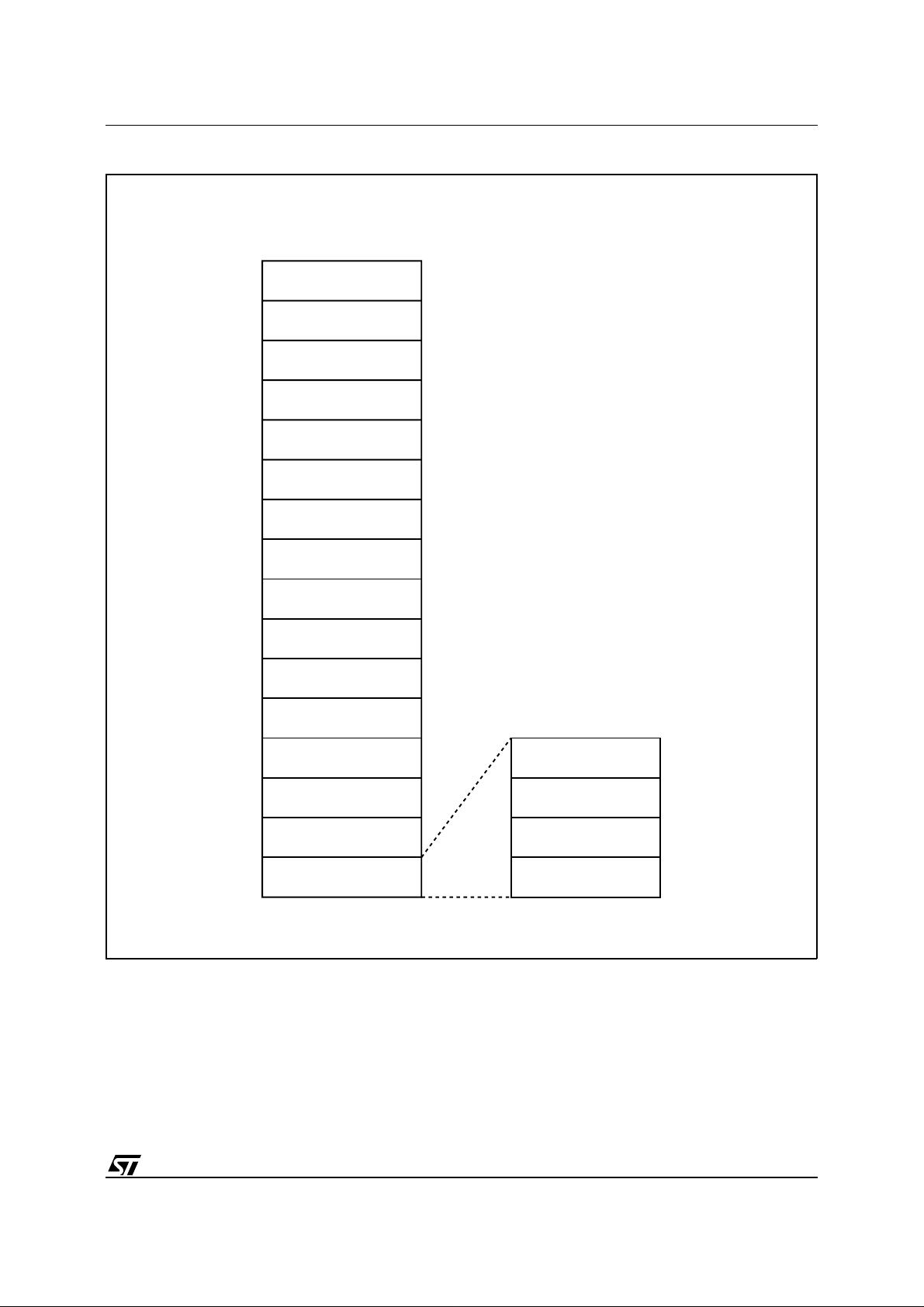
Figure 3B. Bottom Boot Block Memory Map and Block Address Table
BOTTOM BOOT BLOCK
Byte-Wide
FFFFFh
FFFFFh
F0000h
EFFFFh
E0000h
DFFFFh
D0000h
CFFFFh
C0000h
BFFFFh
B0000h
AFFFFh
A0000h
9FFFFh
90000h
8FFFFh
80000h
7FFFFh
70000h
6FFFFh
60000h
5FFFFh
50000h
4FFFFh
40000h
3FFFFh
30000h
2FFFFh
20000h
1FFFFh
10000h
0FFFFh
00000h
64K MAIN BLOCK
64K MAIN BLOCK
64K MAIN BLOCK
64K MAIN BLOCK
64K MAIN BLOCK
64K MAIN BLOCK
64K MAIN BLOCK
64K MAIN BLOCK
64K MAIN BLOCK
64K MAIN BLOCK
64K MAIN BLOCK
64K MAIN BLOCK
64K MAIN BLOCK
64K MAIN BLOCK
64K MAIN BLOCK
32K MAIN BLOCK
8K PARAMETER BLOCK
8K PARAMETER BLOCK
16K BOOT BLOCK
M29W008T, M29W008B
Byte-Wide
0FFFFh
08000h
07FFFh
06000h
05FFFh
04000h
03FFFh
00000h
AI02136
5/30
Page 6
M29W008T, M29W008B
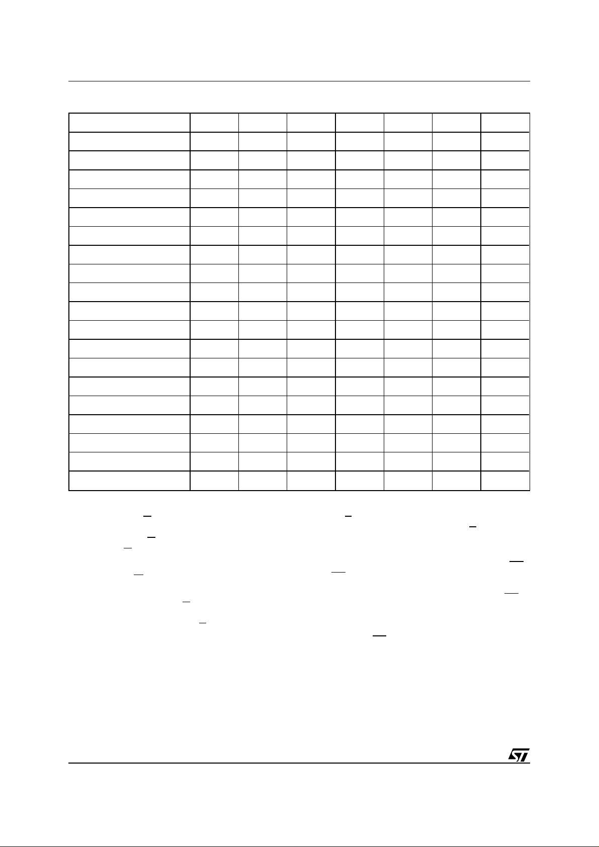
T ab le 3A. M29W008T Block Address Table
Address Range A19 A18 A17 A16 A15 A14 A13
00000h-0FFFFh 0 0 0 0 X X X
10000h-1FFFFh 0 0 0 1 X X X
20000h-2FFFFh 0 0 1 0 X X X
30000h-3FFFFh 0 0 1 1 X X X
40000h-4FFFFh 0 1 0 0 X X X
50000h-5FFFFh 0 1 0 1 X X X
60000h-6FFFFh 0 1 1 0 X X X
70000h-7FFFFh 0 1 1 1 X X X
80000h-8FFFFh 1 0 0 0 X X X
90000h-9FFFFh 1 0 0 1 X X X
A0000h-AFFFFh 1 0 1 0 X X X
B0000h-BFFFFh 1 0 1 1 X X X
C0000h-CFFFFh 1 1 0 0 X X X
D0000h-DFFFFh 1 1 0 1 X X X
E0000h-EFFFFh 1 1 1 0 X X X
F0000h-F7FFFh 1 1 1 1 0 X X
F8000h-F9FFFh 1 1 1 1 1 0 0
FA000h-FBFFFh 1 1 1 1 1 0 1
FC000h-FFFFFh 1 1 1 1 1 1 X
The Output Enable gates the
Output Enable (
G).
outputs through the data buffers during a read
operation. When
impedance.
G is High the outputs are High
G must be forced to VID level during
Block Protection and Unprotection operations.
Write Enable (
This input controls writing to the
W).
Command Register and Address and Data latches.
Ready/Busy Output (R
Ready/Busy is an
B).
open-drain output and gives the internal state of the
P/E.C. of the device. When R
B is Low, the device
is Busy with a Program or Erase operation and it
When R
Program or Erase operation. T he R
High when the memory is put in Erase Suspend or
Standby modes.
Reset/Block Temporary Unprotect Input (
The
tected block(s) temporary unprotection functions.
Reset of the memory is acheived by pulling
V
if the memory is in Read or Standby modes, it will
be available for new operations in t
rising edge of
B is High, the device is ready for any Read,
RP Input provides hardware reset and pro-
for at least t
IL
. When the reset pulse is given,
PLPX
RP.
will not accept any additional program or erase
instructions except the Erase Suspend instruction.
B will also be
RP).
RP to
after the
PHEL
6/30
Page 7
M29W008T, M29W008B
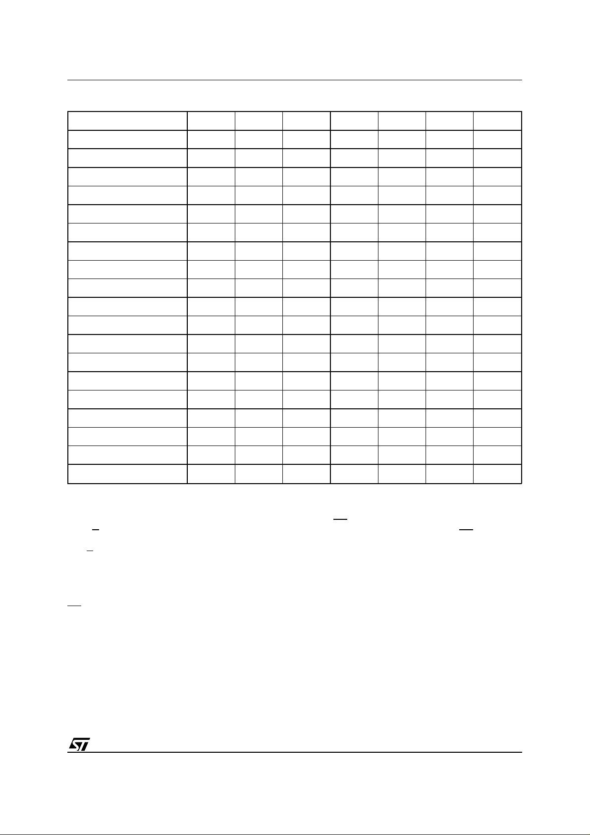
T ab le 3B. M29W008B Block Address Table
Address Range A19 A18 A17 A16 A15 A14 A13
00000h-03FFFh 0 0 0 0 0 0 X
04000h-05FFFh 0 0 0 0 0 1 0
06000h-07FFFh 0 0 0 0 0 1 1
08000h-0FFFFh 0 0 0 0 1 X X
10000h-1FFFFh 0 0 0 1 X X X
20000h-2FFFFh 0 0 1 0 X X X
30000h-3FFFFh 0 0 1 1 X X X
40000h-4FFFFh 0 1 0 0 X X X
50000h-5FFFFh 0 1 0 1 X X X
60000h-6FFFFh 0 1 1 0 X X X
70000h-7FFFFh 0 1 1 1 X X X
80000h-8FFFFh 1 0 0 0 1 X X
90000h-9FFFFh 1 0 0 1 X X X
A0000h-AFFFFh 1 0 1 0 X X X
B0000h-BFFFFh 1 0 1 1 X X X
C0000h-CFFFFh 1 1 0 0 X X X
D0000h-DFFFFh 1 1 0 1 X X X
E0000h-6FFFFh 1 1 1 0 X X X
F0000h-FFFFFh 1 1 1 1 X X X
If the memory is in Erase, Erase Suspend or Program modes the reset will take t
B signal will be held at VIL. The end of the
the R
during which
PLYH
memory reset will be indicated by the rising edge
B. A hardware reset during an Erase or Pro-
of R
gram operation will corrupt the data being programmed or the sector(s) being erased. See Table
14 and Figure 9.
Temporary block unprotection is made by holding
RP at VID. In this condition previously protected
blocks can be programmed or erased. The transi-
RP from VIH to VID must slower than t
tion of
(See Table 15 and Figure 9). When
from V
to VIH all blocks temporarily unprotected
ID
will be again protected.
Supply Voltage.
V
CC
The power supply for all
operations (Read, Program and Erase).
is the reference for all voltage
Ground.
V
SS
V
SS
measurements.
RP is returned
PHPHH
.
7/30
Page 8

M29W008T, M29W008B
DEVICE O PERATIONS
See Tables 4, 5 and 6.
Read operations are used to output the
Read.
contents of the Memory Array, the Electronic Signature, the Status Register or the Block Protection
Status. Both Chip Enable
E and Output Enable G
must be low in order to read the output of the
memory.
Write operations are used to give Instruction
Write.
Commands to the memory or to latch input data to
be programmed. A write operation is initiated when
Chip Enable
with Output Enable
on the falling edge of
E is Low and Write Enable W is Low
G High. Addresses are latched
W or E whichever occurs last.
Commands and Input Data are latched on the rising
edge of
Output Disable.
ance when the Output Enable
Enable
Standby.
Enable
W or E whichever occurs first.
The data outputs are high imped-
G is High with Write
W High.
The memory is in standby when Chip
E is High and the P/E .C. is idle. T he power
consumption is reduced to the standby level and
the outputs are high impedance, independent of
the Output Enable
Automatic Standby.
G or Write Enable W inputs.
After 150ns of bus inactivity
and when CMOS levels are driving the addresses,
the chip automatically enters a pseudo-standby
mode where consumption is reduced to the CMOS
standby value, while outputs still drive the bus.
Electronic S ignature.
Two codes identifying the
manufacturer and the device can be read from the
memory. The manufacturer’s code for STMicroelectronics is 20h, the device code is D2h for the
M29W008T (Top Boot) and DCh for the
M29W008B (Bottom Boot). These codes allow programming equipment or applications to aut omatically match their interface to the characteristics of
the M29W008. The Electronic Signature is output
by a Read operation when the voltage applied to
A9 is at V
and address inputs A1 is Low. The
ID
manufacturer code is output when the Address
input A0 is Low and the device code when this input
is High. Other Address inputs are ignored. The
Electronic Signature can also be read, without raising A9 to V
, by giving the memory the Instruction
ID
AS.
Block Protection.
Each block can be separately
protected against Program or Erase on programming equipment. Block protection provides additional data security, as it disables all program or
erase operations. This mode is activated when both
A9 and
G are raised to VID and an address in the
block is applied on A13-A19. Block protection is
initiated on the edge of
a delay of 100µs, the edge of
W falling to VIL. Then after
W rising to VIH ends
the protection operations. Block protection verify is
achieved by bringing
, while W is at VIH and A9 at VID. Under these
to V
IH
G, E, A0 and A6 to VIL and A1
conditions, reading the data output will yield 01h if
the block defined by the inputs on A13-A19 is
protected. Any attempt to program or erase a protected block will be ignored by the device.
Block Temporary Unprotection.
Any previously
protected block can be temporarily unprot ected in
order to change stored data. The temporary unprotection mode is activated by bringing
RP to VID.
During the temporary unprotection mode the previously protected blocks are unprotected. A block
can be selected and data can be modified by
executing the Erase or Program instruction with the
RP signal held at VID. When RP is returned to VIH,
all the previously protected blocks are again protected.
Block Unprotection.
All protected blocks can be
unprotected on programming equipment to allow
updating of bit contents. All blocks must first be
protected before the unprotection operation. Block
unprotection is activated when A9,
and A12, A15 at VIH. Unprotection is initiated
V
ID
by the edge of
W falling to VIL. After a delay of 10ms,
G and E are at
the unprotection operation will end. Unprotection
verify is achieved by bringing
A0 is at V
at V
ID
, A6 and A1 are at VIH and A9 remains
IL
. In these conditions, reading the output data
G and E to VIL while
will yield 00h if the block defined by the inputs
A13-A19 has been succesfully unprotected. Each
block must be separately verified by giving its address in order to ensure that it has been unprotected.
8/30
Page 9
M29W008T, M29W008B
T ab le 4. User Bus Operations
(1)
Operation E G W RP A0 A1 A6 A9 A12 A15 DQ0-DQ7
Read Byte V
Write Byte V
Output Disable V
Standby V
Reset X X X V
Block
Protection
(2,4)
Blocks
Unprotection
VIL VIDVIL Pulse V
V
(4)
V
IL
IL
IL
IH
ID
IL
V
IH
V
IH
XXVIHXXXXXX Hi-Z
V
ID
V
IH
V
IL
V
IH
VIL Pulse V
V
V
V
A0 A1 A6 A9 A12 A15 Data Output
IH
A0 A1 A6 A9 A12 A15 Data Input
IH
IH
IH
IH
XXXXXX Hi-Z
XXXXXX Hi-Z
IL
XXXVIDXX X
XXXVIDV
V
IH
IH
Block
Protection
(2,4)
Verify
V
V
IL
IL
V
IH
V
V
IH
V
IL
V
IH
V
IL
ID
A12 A15
Protect
Status
Block
Unprotection
(2,4)
Verify
V
V
IL
IL
V
IH
V
V
IH
V
IL
V
IH
V
IH
ID
A12 A15
Protect
Status
Block
Temporary
XX XV
ID
XXXXXX X
Unprotection
Notes:
1. X = V
2. Block Address must be given on A13-A19 bits.
3. See Table 6.
4. Operation performed on programming equipment.
IL
or V
IH
X
Block
(3)
Block
(3)
T able 5. Read Electronic Signature (following AS instruction or with A9 = VID)
Code Device E G WA0A1
Manufact. Code V
Device Code
M29W008T V
M29W008B V
IL
IL
IL
V
IL
V
IL
V
IL
V
IH
V
IH
V
IH
V
IL
V
IH
V
IH
V
IL
V
IL
V
IL
T ab le 6. Read Block Protection with AS Instruction
Code E G W A0 A1 A13-A19
Protected Block V
Unprotected Block V
IL
IL
V
IL
V
IL
V
IH
V
IH
V
IL
V
IL
V
IH
V
IH
Block Address Don’t Care 01h
Block Address Don’t Care 00h
Addresses
Other
Addresses
Don’t Care 20h
Don’t Care D2h
Don’t Care DCh
Other
DQ0-DQ7
DQ0-
DQ7
9/30
Page 10

M29W008T, M29W008B
INSTRUCTIONS AND COMMANDS
The Command Interface latches commands wr itten to the memory. Instructions are made up from
one or more commands to perform Read Memory
Array, Read Electronic Signature, Read B lock Protection, Program, Block Erase, Chip Erase, Erase
Suspend and Erase Resume. Commands are
made of address and data sequences. The instructions require from 1 to 6 cycles, the first or first
three of which are always write operations used to
initiate the instruction. They are followed by either
further write cycles to confirm the first command or
execute the command immediately . Command sequencing must be followed exactly. Any invalid
combination of commands will reset the device to
Read Array. The increased number of cycles has
been chosen to assure maximum data security.
Instructions are initialised by two initial Coded cycles which unlock the Command Interface. In addition, for Erase, instruction confirmation is again
preceded by the two Coded cycles.
Status Register Bits
P/E.C. status is indicated during execution by Data
Polling on DQ7, detection of Toggle on DQ6 and
DQ2, or Error on DQ5 and Erase Timer DQ3 bits.
Any read attempt during Program or Erase command execution will automatically output these five
Status Register bits. The P/E.C. automatically sets
T ab le 7. Commands
Hex Code Command
00h Invalid/Reserved
10h Chip Erase Confirm
20h Reserved
30h Block Erase Resume/Confirm
80h Set-up Erase
90h
A0h Program
B0h Erase Suspend
F0h Read Array/Reset
Read Electronic Signature/
Block Protection Status
bits DQ2, DQ3, DQ5, DQ6 and DQ7. Other bits
(DQ0, DQ1 and DQ4) are reser ved for future use
and should be masked. See Tables 9 and 10.
Data Polling Bit (DQ7).
When Programming operations are in progress, this bit outputs t he complement of the bit being programmed on DQ7.
During Erase operation, it outputs a ’0’. After completion of the operation, DQ7 will output the bit last
programmed or a ’1’ after erasing. Data Polling is
valid and only effective during P/E.C. operation,
that is after the fourth
after the sixth
W pulse for erase. It must be per-
W pulse for programming or
formed at the address being programmed or at an
address within the block being erased. If all the
blocks selected for erasure are protected, DQ7 will
be set to ’0’ for about 100µs, and then return to the
previous addressed memory data value. See Figure 11 for the Data Polling flowchart and Figure 10
for the Data Polling waveforms. DQ7 will also flag
the Erase Suspend mode by switching from ’0’ to
’1’ at the start of the Erase Suspend. In order to
monitor DQ7 in the Erase Suspend mode an address within a block being erased must be provided. For a Read Operation in Erase Suspend
mode, DQ7 will output ’1’ if the read is attempted
on a block being erased and the data value on other
blocks. During Program operation i n Erase Suspend Mode, DQ7 will have the same behaviour as
in the normal program execution outside of the
suspend mode.
Toggle Bit (DQ6).
When Programming or Erasing
operations are in progress, successive attempts to
read DQ6 will output complementary data. DQ6 will
toggle following toggling of either
G, or E when G
is low. The operation is completed when two successive reads yield the same output data. The next
read will output the bit last programmed or a ’1’ after
erasing. The toggle bit DQ6 is valid only during
P/E.C. operations, that is after the fourth
for programming or after the sixth
W pulse
W pulse for
Erase. If the blocks selected for erasure are protected, DQ6 will toggle for about 100µs and then
return back to Read. DQ6 will be set to ’1’ if a Read
operation is attempted on an Erase Suspend block.
When erase is suspended DQ6 will toggle during
programming operations in a block different to the
block in Erase Suspend. Either
E or G toggling will
cause DQ6 to toggle. See Figure 12 for Toggle Bit
flowchart and Figure 13 for Toggle Bit waveforms.
10/30
Page 11

M29W008T, M29W008B
T ab le 8. Instructions
(1)
Mne. Instr. Cyc. 1st Cyc. 2nd Cyc. 3rd Cyc. 4th Cyc. 5th Cyc. 6th Cyc. 7th Cyc.
(3,7)
Addr.
RD
(2,4)
Read/Reset
Memory
Array
1+
3+
Data
Addr.
(3,7)
Data
(3,7)
Addr.
AS
(4)
Auto Select 3+
Data
(3,7)
Addr.
PG Program 4
Data
(3,7)
Addr.
BE Block Erase
6
Data
(3,7)
Chip Erase 6
CE
Addr.
Data
(3,7)
Addr.
Data
Addr.
Data
(3,7)
IL
ES
Notes:
Suspend
Erase
ER
Resume
1. Commands not interpreted in this table will default to read array mode.
2. A wait of t
before starting any new operation. (See Table 14 and Figure 9).
3. X = Don’t Care.
4. The first cycles of the RD or AS instructions are followed by read operations. Any number of read cycles can occur after
the command cycles.
5. Signature Address bits A0, A1 at V
Device code.
6. Block Protection Address: A0 at V
7. For Coded cycles address inputs A15-A19 are don’t care.
8. Optional, additional Blocks addresses must be entered within the erase timeout delay after last write entry, timeout status
can be verified through DQ3 value (see Erase Timer Bit DQ3 description). When full command is entered,
read Data Polling or Toggle bit until Erase is completed or suspended.
9. Read Data Polling, T oggle bits or R
10.During Erase Suspend, Read and Data Program functions are allowed in blocks not being erased.
PLYH
1
1
is necessary after a Read/Reset command if the memory was in an Erase or Program mode
Erase
(10)
X
Read Memory Array until a new write cycle is initiated.
F0h
5555h 2AAAh 5555h
AAh 55h F0h
Read Memory Array until a new write cycle
is initiated.
5555h 2AAAh 5555h Read Electronic Signature or Block
Protection Status until a new write cycle is
AAh 55h 90h
5555h 2AAAh 5555h
AAh 55h A0h
5555h 2AAAh 5555h 5555h 2AAAh
initiated. See Note 5 and 6.
Program
Address
Program
Read Data Polling or Toggle Bit
until Program completes.
Data
Block
Address
AAh 55h 80h AAh 55h 30h 30h
5555h 2AAAh 5555h 5555h 2AAAh 5555h
AAh 55h 80h AAh 55h 10h
X
Read until Toggle stops, then read all the data needed from any
B0h
30h
will output Manufacturer code (20h). Address bits A0 at VIH and A1 at VIL will output
IL
, A1 at VIH and A13-A19 within the Block will output the Block Pr otec tio n st atus.
B until Erase completes.
Block(s) not being erased then Resume Erase.
X
Read Data Polling or Toggle Bits until Erase completes or Erase
is suspended another time
Additional
Block
Note 9
(8)
11/30
Page 12

M29W008T, M29W008B
Table 9. Status Register Bits
DQ Name Logic Level Definition Note
Data
7
Polling
6 Toggle Bit
5 Error Bit
4 Reserved
Erase
3
Time Bit
2 Toggle Bit
’1’
’0’ Erase On-going
DQ
DQ Program On-going
’-1-0-1-0-1-0-1-’ Erase or Program On-going Successive reads output complementary
DQ Program Complete
’-1-1-1-1-1-1-1-’
’1’ Program or Erase Error
’0’ Program or Erase On-going
’1’ Erase Timeout Period Expired
’0’
’-1-0-1-0-1-0-1-’
1
DQ
Erase Complete or erase
block in Erase Suspend
Program Complete or data
of non erase block during
Erase Suspend
Erase Complete or Erase
Suspend on currently
addressed block
Erase Timeout Period
On-going
Chip Erase, Erase or Erase
Suspend on the currently
addressed block.
Erase Error due to the
currently addressed block
(when DQ5 = ’1’).
Program on-going, Erase
on-going on another block or
Erase Complete
Erase Suspend read on
non Erase Suspend block
Indicates the P/E.C. status, check during
Program or Erase, and on completion
before checking bits DQ5 for Program or
Erase Success.
data on DQ6 while Programming or Erase
operations are on-going. DQ6 remains at
constant level when P/E.C. operations are
completed or Erase Suspend is
acknowledged.
This bit is set to ’1’ in the case of
Programming or Erase failure.
P/E.C. Erase operation has started. Only
possible command entry is Erase Suspend
(ES).
An additional block to be erased in parallel
can be entered to the P/E.C.
Indicates the erase status and allows to
identify the erased block
1 Reserved
0 Reserved
Notes:
Logic level ’1’ is High, ’0’ is Low. -0-1-0-0-0-1-1-1-0- represent bit value in successive Read operations.
12/30
Page 13

M29W008T, M29W008B
T able 10. Polling and T oggle Bits
Mode DQ7 DQ6 D Q2
Program
Erase 0 Toggle Note 1
Erase Suspend Read
(in Erase Suspend
block)
Erase Suspend Read
(outside Erase Suspend
block)
Erase Suspend Program
Note:
1. Toggle if the address is within a block being erased.
’1’ if the address is within a block not being erased.
Toggle Bit (DQ2).
This toggle bit, together with
DQ7 Toggle 1
1 1 Toggle
DQ7 DQ6 DQ2
DQ7 Toggle N/A
DQ6, can be used to determine the dev ice status
during the Erase operations. It can also be used to
identify the block being erased. During Erase or
Erase Suspend a read from a block being erased
will cause DQ2 to toggle. A read from a block not
being erased will set DQ2 to ’1’ during erase and
to DQ2 during Erase Suspend. During Chip Erase
a read operation will cause DQ2 to toggle as all
blocks are being erased. DQ2 will be set to ’1’
during program operation and when erase is complete. After erase completion and if the error bit
DQ5 is set to ’1’, DQ2 will toggle if the faulty block
is addressed.
Error Bit (DQ5).
This bit is set to ’1’ by the P/E.C.
when there is a failure of programming, block
erase, or chip erase that results in invalid data in
the memory block. In case of an er ror in block erase
or program, the block in which the error occured or
to which the programmed data belongs, must be
discarded. The DQ5 failure condition will also appear if a user tries to program a ’1’ to a location that
is previously programmed to ’0’. Other Blocks may
still be used. The error bit resets after a Read/Reset
(RD) instruction. In case of success of Program or
Erase, the error bit will be set to ’0’ .
Erase Timer Bit (DQ3).
This bit is set to ’0’ by the
P/E.C. when the last block Erase command has
been entered to the Command Interface and it is
awaiting the Erase start. When the erase timeout
period is finished, after 50µs to 90µs, DQ3 returns
to ’1’.
Coded Cycles
The two Coded cycles unlock the C ommand Interface. They are followed by an input command or a
confirmation command. The Coded cycles consist
of writing the data AAh at address 5555h during the
first cycle. During the second cycle the Coded
cycles consist of writing the data 55h at address
2AAAh. A0 to A15 are valid, other address lines are
’don’t care’. The Coded cycles happen on first and
second cycles of the command write or on the
fourth and fifth cycles.
Instructions
See Table 8.
Read/Reset (RD) Instruction.
The Read/Reset
instruction consists of one write cycle giving the
command F0h. It can be optionally preceded by the
two Coded cycles. Subsequent read operations will
read the memory array addressed and output the
data read. A wait state of 10µs is necessary after
Read/Reset prior to any valid read if the memory
was in an Erase mode when the RD instruc tion is
given.
Auto Select (AS) Instruction.
This instruction
uses the two Coded cycles followed by one write
cycle giving the command 90h to address 555h for
command set-up. A subsequent read will output the
manufacturer code and the device code or the
block protection status depending on the levels of
A0 and A1. The manufacturer code, 20h, is output
when the addresses lines A0 and A1 are Low, the
device code, EAh for Top Boot, EBh for Bottom
Boot is output when A0 is High with A1 Low.
The AS instruction also allows access to the block
protection status. After giving the AS instruction, A0
and A6 are set to V
with A1 at VIH, while A13-A19
IL
define the address of the bloc k to be verified. A read
in these conditions will output a 01h if the block is
protected and a 00h if the block is not protected.
Program (PG) Instruction.
This instruction uses
four write cycles. The Program command A0h is
written to address 5555h on the third cyc le after two
Coded cycles. A fourth write operation latches the
Address on the falling edge of
W or E and the Data
to be written on the rising edge and starts the
P/E.C. Read operations output the Status Register
bits after the programming has started. Memory
programming is made only by writing ’0’ in place of
’1’. Status bits DQ6 and DQ7 determine if programming is on-going and DQ5 allows verification of any
possible error. Programming at an address not in
blocks being erased is also possible during erase
suspend. In this case, DQ2 will toggle at the address being programmed.
13/30
Page 14

M29W008T, M29W008B
T ab le 11. AC Measurement Conditions
Input Rise and Fall Times
10ns
≤
Figure 5. AC Testing Load Circuit
0.8V
Input Pulse Voltages 0 to 3V
Input and Output Timing Ref. Voltages 1.5V
Figure 4. AC Testing Input O utput Waveform
3V
1.5V
0V
AI01417
(1)
T ab le 12. Capacitance
(TA = 25 °C, f = 1 MHz )
DEVICE
UNDER
TEST
CL includes JIG capacitance
1N914
3.3kΩ
CL = 30pF or 100pF
Symbol Parameter Test Condition Min Max Unit
C
IN
C
OUT
Note:
1. Sampled only, not 100% tested.
Input Capacitance VIN = 0V 6 pF
Output Capacitance V
= 0V 12 pF
OUT
OUT
AI01968
T ab le 13. DC Characteristics
(T
= 0 to 70°C, –20 to 85°C or –40 to 85°C; VCC = 2.7V to 3.6V)
A
Symbol Parameter Test Condition Min Max Unit
I
Note:
I
I
CC1
I
CC3
CC4
V
V
V
V
V
V
I
LO
I
LKO
Input Leakage Current 0V ≤ VIN ≤ V
LI
Output Leakage Current 0V ≤ V
OUT
≤ V
CC
CC
Supply Current (Read) Byte E = VIL, G = VIH, f = 6MHz 10 mA
Supply Current (Standby) E = VCC ± 0.2V 100
(1)
Supply Current (Program or Erase)
Input Low Voltage –0.5 0.8 V
IL
Input High Voltage 0.7 VCC VCC + 0.3 V
IH
Output Low Voltage IOL = 1.8mA 0.45 V
OL
Output High Voltage CMOS IOH = –100µAV
OH
A9 Voltage (Electronic Signature) 11.5 12.5 V
ID
A9 Current (Electronic Signature) A9 = V
ID
Supply Voltage (Erase and
Program lock-out)
1. Sampled only, not 100% tested.
Byte program, Block or
Chip Erase in progress
ID
–0.4V V
CC
2.0 2.3 V
1
±
1
±
20 mA
100
A
µ
A
µ
A
µ
A
µ
14/30
Page 15

T ab le 14A. Read AC Characteristics
(T
= 0 to 70°C, –20 to 85°C or –40 to 85°C)
A
M29W008T, M29W008B
M29W008T / M29W008B
Symbol Alt Parameter
Test
Condition
V
-90 -100
= 3.0V to 3.6V
CC
C
= 30pF
L
Min Max Min Max
t
AVAV
t
AVQV
t
ELQX
t
ELQV
t
GLQX
t
GLQV
t
EHQX
t
EHQZ
t
GHQX
t
GHQZ
t
AXQX
t
PLYH
t
PHEL
t
PLPX
Notes:
t
Address Valid to Next Address Valid
RC
t
Address Valid to Output Valid
ACC
(1)
(2)
(1)
(2)
(1)
(1)
(1,3)
1. Sampled only, not 100% tested.
G may be delayed by up to t
2.
3. To be considered only if the Reset pulse is given while the memory is in Erase, Erase Suspend or Program mode.
Chip Enable Low to Output
t
LZ
Transition
t
Chip Enable Low to Output Valid G = V
CE
Output Enable Low to Output
t
OLZ
Transition
t
Output Enable Low to Output Valid E = V
OE
Chip Enable High to Output
t
OH
Transition
tHZChip Enable High to Output Hi-Z G = V
Output Enable High to Output
t
OH
Transition
tDFOutput Enable High to Output Hi-Z E = V
Address Transition to Output
t
OH
Transition
t
RRB
RP Low to Read Mode 10 10
t
READY
t
RP High to Chip Enable Low 50 50 ns
RH
t
RP Pulse Width 500 500 ns
RP
- t
ELQV
after the falling edge of E without increasing t
GLQV
E = VIL,
G = V
E = VIL,
G = V
G = V
E = V
G = V
E = V
E = VIL,
G = V
IL
IL
IL
IL
IL
IL
IL
IL
IL
IL
IL
90 100 ns
90 100 ns
00ns
90 100 ns
00ns
35 40 ns
00ns
30 30 ns
00ns
30 30 ns
00ns
.
ELQV
= 2.7V to 3.6V
V
CC
C
= 30pF
L
Unit
µ
s
15/30
Page 16

M29W008T, M29W008B
T ab le 14B. Read AC Characteristics
(T
= 0 to 70°C, –20 to 85°C or –40 to 85°C)
A
M29W008T / M29W008B
Symbol Alt Parameter
t
AVAV
t
AVQV
t
ELQX
t
ELQV
t
GLQX
t
GLQV
t
EHQX
t
EHQZ
t
GHQX
t
GHQZ
t
AXQX
t
PLYH
t
PHEL
t
PLPX
Notes:
t
Address Valid to Next Address Valid
RC
t
Address Valid to Output Valid
ACC
(1)
(2)
(1)
(2)
(1)
(1)
(1,3)
1. Sampled only, not 100% tested.
G may be delayed by up to t
2.
3. To be considered only if the Reset pulse is given while the memory is in Erase, Erase Suspend or Program mode.
Chip Enable Low to Output
t
LZ
Transition
t
Chip Enable Low to Output Valid G = V
CE
Output Enable Low to Output
t
OLZ
Transition
t
Output Enable Low to Output Valid E = V
OE
Chip Enable High to Output
t
OH
Transition
tHZChip Enable High to Output Hi-Z G = V
Output Enable High to Output
t
OH
Transition
tDFOutput Enable High to Output Hi-Z E = V
Address Transition to Output
t
OH
Transition
t
RRB
RP Low to Read Mode 10 10
t
READY
t
RP High to Chip Enable Low 50 50 ns
RH
t
RP Pulse Width 500 500 ns
RP
- t
ELQV
after the falling edge of E without increasing t
GLQV
Test
Condition
E = VIL,
G = V
IL
E = VIL,
G = V
IL
G = V
IL
IL
E = V
IL
IL
G = V
IL
IL
E = V
IL
IL
E = VIL,
G = V
IL
-120 -150
VCC = 2.7V to 3.6V VCC = 2.7V to 3.6V
Min Max Min Max
120 150 ns
120 150 ns
00ns
120 150 ns
00ns
50 55 ns
00ns
30 40 ns
00ns
30 40 ns
00ns
.
ELQV
Unit
µ
s
16/30
Page 17

Figure 6. Read Mode AC Waveforms
tEHQZ
tGHQZ
tGHQX
M29W008T, M29W008B
AI02191
VALID
tAVAV
VALID
A0-A19
tAVQV tAXQX
tELQV
tGLQV
tGLQX
tELQX tEHQX
E
G
DQ0-DQ7
OUTPUT ENABLE DATA VALID
ADDRESS VALID
AND CHIP ENABLE
W) = High.
Write Enable (
Note:
17/30
Page 18

M29W008T, M29W008B
Tabl e 15A. Write AC Characteristics, Write Enable Controlled
= 0 to 70°C, –20 to 85°C or –40 to 85°C)
(T
A
Symbol Alt Parameter
V
= 3.0V to 3.6V
CC
C
Min Max Min Max
t
AVAV
t
ELWL
t
WLWH
t
DVWH
t
WHDX
t
WHEH
t
WHWL
t
AVWL
t
WLAX
t
GHWL
t
VCHEL
t
WHGL
t
PHPHH
t
PLPX
t
WHRL
t
PHWL
Notes:
1. Sample only, not 100% tested.
2. This timing is for Temporary Block Unprotection operation.
t
Address Valid to Next Address Valid 90 100 ns
WC
tCSChip Enable Low to Write Enable Low 0 0 ns
t
Write Enable Low to Write Enable High 45 50 ns
WP
t
Input Valid to Write Enable High 45 50 ns
DS
t
Write Enable High to Input Transition 0 0 ns
DH
t
Write Enable High to Chip Enable High 0 0 ns
CH
t
Write Enable High to Write Enable Low 30 30 ns
WPH
t
Address Valid to Write Enable Low 0 0 ns
AS
t
Write Enable Low to Address Transition 45 50 ns
AH
Output Enable High to Write Enable Low 0 0 ns
t
t
(1,2)
t
(1)
t
BUSY
(1)
t
VCSVCC
OEH
VIDR
t
RP
RSP
High to Chip Enable Low 50 50
Write Enable High to Output Enable Low 0 0 ns
RP Rise Time to V
ID
500 500 ns
RP Pulse Width 500 500 ns
Program Erase Valid to RB Delay 90 90 ns
RP High to Write Enable Low 4 4
M29W008T / M29W008B
-90 -100
= 2.7V to 3.6V
V
CC
= 30pF
L
C
= 30pF
L
Unit
µ
µ
s
s
Block Erase (BE) Instruction
. This instruction
uses a minimum of six write cycles. The Erase
Set-up command 80h is written to address 5555h
on third cycle after the two Coded cycles. The Block
Erase Confirm command 30h is similarly written on
the sixth cycle after another two Coded cycles.
During the input of the second command an address within the block to be erased is given a nd
latched into the memory. Additional block Erase
Confirm commands and block addresses can be
written subsequently to erase other blocks in parallel, without further Coded cycles. The erase will
start after the erase timeout period (see Erase
Timer Bit DQ3 description). Thus, additional Erase
Confirm commands for other blocks must be given
18/30
within this delay . The input of a new E rase Confirm
command will restart the timeout period. The status
of the internal timer can be monitored through the
level of DQ3, if DQ3 is ’0’ the Block Erase Command has been given and the timeout is running, if
DQ3 is ’1’, the timeout has expired and the P/E.C.
is erasing the Block(s). If the second command
given is not an erase confirm or if the Coded cycles
are wrong, the instruction aborts, and the device is
reset to Read Array. It is not necessary to program
the block with 00h as the P/E.C. will do t his automatically before to erasing to FFh. Read operations
after the sixth rising edge of
W or E output the
status register status bits.
Page 19

M29W008T, M29W008B
Tabl e 15B. Write AC Characteristics, Write Enable Controlled
= 0 to 70°C, –20 to 85°C or –40 to 85°C)
(T
A
Symbol Alt Parameter
VCC = 2.7V to 3.6V VCC = 2.7V to 3.6V
Min Max Min Max
t
AVAV
t
ELWL
t
WLWH
t
DVWH
t
WHDX
t
WHEH
t
WHWL
t
AVWL
t
WLAX
t
GHWL
t
VCHEL
t
WHGL
t
PHPHH
t
PLPX
t
WHRL
t
PHWL
Notes:
1. Sample only, not 100% tested.
2. This timing is for Temporary Block Unprotection operation.
t
t
t
t
(1,2)
t
(1)
t
BUSY
(1)
t
Address Valid to Next Address Valid 120 150 ns
WC
t
Chip Enable Low to Write Enable Low 0 0 ns
CS
t
Write Enable Low to Write Enable High 50 65 ns
WP
t
Input Valid to Write Enable High 50 65 ns
DS
t
Write Enable High to Input Transition 0 0 ns
DH
t
Write Enable High to Chip Enable High 0 0 ns
CH
Write Enable High to Write Enable Low 30 35 ns
WPH
t
Address Valid to Write Enable Low 0 0 ns
AS
t
Write Enable Low to Address Transition 50 65 ns
AH
Output Enable High to Write Enable Low 0 0 ns
VCSVCC
OEH
VIDR
t
RP
High to Chip Enable Low 50 50
Write Enable High to Output Enable Low 0 0 ns
RP Rise Time to V
ID
500 500 ns
RP Pulse Width 500 500 ns
Program Erase Valid to RB Delay 90 90 ns
RP High to Write Enable Low 4 4
RSP
M29W008T / M29W008B
-120 -150
Unit
µ
µ
s
s
During the execution of the erase by the P/E.C., the
memory accepts only the Erase Suspend ES and
Read/Reset RD instructions. Data Polling bit DQ7
returns ’0’ while the erasure is in progress and ’1’
when it has completed. The Toggle bit DQ2 and
DQ6 toggle during the erase operation. They stop
when erase is completed. After completion the
Status Register bit DQ5 returns ’1’ if there has been
an erase failure. In such a situation, the Toggle bit
DQ2 can be used to determine which block is not
correctly erased. In the case of erase failure, a
Read/Reset RD instruction is necessary in order to
reset t he P/E.C.
Chip Erase (CE ) Instruction.
This instruction uses
six write cycles. The Erase Set-up command 80h
is written to address 5555h on the third cycle after
the two Coded cycles. The Chip Erase Confirm
command 10h is similarly written on the sixth cycle
after another two Coded cycles. If the second
command given is not an erase confirm or if the
Coded cycles are wrong, the instruction aborts and
the device is reset to Read Array. It is not necessary
to program the array with 00h first as the P/E.C. will
automatically do this before erasing it to FFh. Read
operations after the sixth rising edge of
W or E
output the Status Register bits. During the execution of the erase by the P/E.C., Data Polling bit DQ7
returns ’0’, then ’1’ on completion. The Toggle bits
DQ2 and DQ6 toggle during erase operation and
stop when erase is completed. After completion the
Status Register bit DQ5 returns ’1’ if there has been
an Erase Failure.
19/30
Page 20

M29W008T, M29W008B
Figure 7. Write AC Waveforms, W Controlled
A0-A19
tAVWL
E
tAVAV
VALID
tWLAX
tWHEH
tELWL
G
W
DQ0-DQ7
V
CC
tVCHEL
RB
Note:
Address are latched on the falling edge of
Erase Suspend (ES) Instruction.
W, Data is latched on the rising edge of W.
The Block
Erase operation may be suspended by this instruction which consists of writing the command B0h
without any specific address. No Coded cycles are
required. It permits reading of data fr om another
block and programming in another block while an
erase operation is in progress. Erase suspend is
accepted only during the Block Erase instruction
execution. Writing this command during Erase
timeout will, in addition to suspending the erase,
terminate the timeout. The Toggle bit DQ6 stops
toggling when the P/E.C. is suspended. The Toggle
bits will stop toggling between 0.1µs and 15µs after
the Erase Suspend (ES) command has been written. The device will then automatically be set to
Read Memory Array mode. When erase is sus-
tWHGL
tWLWHtGHWL
tWHWL
tDVWH
VALID
tWHRL
tWHDX
AI02192
pended, a Read from blocks being erased will
output DQ2 toggling and DQ6 at ’1’. A Read from
a block not being erased returns valid data. During
suspension the memory will respond only to the
Erase Resume ER and the Program PG instructions. A Program operation can be initiated during
erase suspend in one of the blocks not being
erased. It will result in both DQ2 and DQ 6 toggling
when the data is being programmed. A Read/Reset
command will definitively abort erasure and result
in invalid data in the blocks being erased.
Erase Resume (ER) Instruction.
If an Erase Suspend instruction was previously executed, the
erase operation may be resumed by giving the
command 30h, at any address, and without any
Coded cycles.
20/30
Page 21

M29W008T, M29W008B
T ab le 16A. Write AC Characteristics, Chip Enable Controlled
= 0 to 70°C, –20 to 85°C or –40 to 85°C)
(T
A
Symbol Alt Parameter
V
= 3.0V to 3.6V
CC
C
Min Max Min Max
t
AVAV
t
WLEL
t
ELEH
t
DVEH
t
EHDX
t
EHWH
t
EHEL
t
AVEL
t
ELAX
t
GHEL
t
VCHWL
t
EHGL
t
PHPHH
t
PLPX
(1)
t
EHRL
(1)
t
PHWL
Notes:
1. Sample only, not 100% tested.
2. This timing is for Temporary Block Unprotection operation.
(1,2)
t
t
t
t
t
t
t
CPH
t
t
t
VCS
t
OEH
t
VIDR
t
t
BUSY
t
RSP
Address Valid to Next Address Valid 90 100 ns
WC
Write Enable Low to Chip Enable Low 0 0 ns
WS
Chip Enable Low to Chip Enable High 45 50 ns
CP
Input Valid to Chip Enable High 45 50 ns
DS
Chip Enable High to Input Transition 0 0 ns
DH
Chip Enable High to Write Enable High 0 0 ns
WH
Chip Enable High to Chip Enable Low 30 30 ns
Address Valid to Chip Enable Low 0 0 ns
AS
Chip Enable Low to Address Transition 45 50 ns
AH
Output Enable High Chip Enable Low 0 0 ns
VCC High to Write Enable Low 50 50
Chip Enable High to Output Enable Low 0 0 ns
RP Rise TIme to V
RP Pulse Width 500 500 ns
RP
ID
500 500 ns
Program Erase Valid to RB Delay 90 90 ns
RP High to Write Enable Low 4 4
M29W008T / M29W008B
V
= 30pF
L
CC
= 2.7V to 3.6V
C
= 30pF
L
Unit-90 -100
s
µ
s
µ
POWER SUPP LY
Power Up
The memory Command Interface is reset on power
up to Read Array . E ither
E or W must be tied to V
during Power Up to allow maximum security and
the possibility to write a command on the first rising
edge of
blocked when Vcc is below V
E and W. Any write cycle initiation is
.
LKO
Supply Rails
Normal precautions must be taken for supply voltage decoupling; each device in a system should
have the V
IH
close to the V
rail decoupled with a 0. 1µF capacitor
CC
and VSS pins. The PCB trace
CC
widths should be sufficient to carry the V
gram and erase currents required.
CC
pro-
21/30
Page 22

M29W008T, M29W008B
T ab le 16B. Write AC Characteristics, Chip Enable Controlled
= 0 to 70°C, –20 to 85°C or –40 to 85°C)
(T
A
Symbol Alt Parameter
V
= 2.7V to 3.6V VCC = 2.7V to 3.6V
CC
Min Max Min Max
t
AVAV
t
WLEL
t
ELEH
t
DVEH
t
EHDX
t
EHWH
t
EHEL
t
AVEL
t
ELAX
t
GHEL
t
VCHWL
t
EHGL
t
PHPHH
t
PLPX
(1)
t
EHRL
(1)
t
PHWL
Notes:
1. Sample only, not 100% tested.
2. This timing is for Temporary Block Unprotection operation.
(1,2)
t
t
t
t
t
t
t
CPH
t
t
t
VCS
t
OEH
t
VIDR
t
t
BUSY
t
RSP
Address Valid to Next Address Valid 120 150 ns
WC
Write Enable Low to Chip Enable Low 0 0 ns
WS
Chip Enable Low to Chip Enable High 50 50 ns
CP
Input Valid to Chip Enable High 50 50 ns
DS
Chip Enable High to Input Transition 0 0 ns
DH
Chip Enable High to Write Enable High 0 0 ns
WH
Chip Enable High to Chip Enable Low 20 20 ns
Address Valid to Chip Enable Low 0 0 ns
AS
Chip Enable Low to Address Transition 50 50 ns
AH
Output Enable High Chip Enable Low 0 0 ns
VCC High to Write Enable Low 50 50
Chip Enable High to Output Enable Low 0 0 ns
RP Rise TIme to V
RP Pulse Width 500 500 ns
RP
ID
500 500 ns
Program Erase Valid to RB Delay 90 90 ns
RP High to Write Enable Low 4 4
M29W008T / M29W008B
-120 -150
Unit
µ
µ
s
s
22/30
Page 23

Figure 8. Write AC Waveforms, E Controlled
M29W008T, M29W008B
tAVAV
A0-A19
W
G
E
DQ0-DQ7
V
CC
RB
tWLEL
tVCHWL
tAVEL
VALID
tELEHtGHEL
tDVEH
VALID
tEHRL
tELAX
tEHWH
tEHGL
tEHEL
tEHDX
AI02193
Note:
Address are latched on the falling edge of
E, Data is latched on the rising edge of E.
Figure 9. Read and Write AC Characteristics, RP Related
E
tPHEL
W
tPHWL
RB
RP
tPLPX
tPLYH
tPHPHH
AI02091
23/30
Page 24

M29W008T, M29W008B
Table 17A. Data Polling and T oggle Bit AC Characteristics
= 0 to 70°C, –20 to 85°C or –40 to 85°C)
(T
A
(1)
M29W008T / M29W008B
Sym-
bol
Parameter
V
CC
Min Max Min Max
t
WHQ7V
t
EHQ7V
t
Q7VQV
t
WHQV
Write Enable High to DQ7 Valid
(Program,
W Controlled)
Write Enable High to DQ7 Valid
(Chip Erase,
W Controlled)
Chip Enable High to DQ7 Valid
(Program,
E Controlled)
Chip Enable High to DQ7 Valid
(Chip Erase,
E Controlled)
Q7 Valid to Output Valid (Data Polling) 35 40 ns
Write Enable High to Output Valid (Program) 10 2400 10 2400
10 2400 10 2400 ms
1.0 60 1.0 60 sec
10 2400 10 2400
1.0 60 1.0 60 sec
Write Enable High to Output Valid (Chip Erase) 1.0 60 1.0 60 sec
t
Chip Enable High to Output Valid (Program) 10 2400 10 2400
EHQV
Chip Enable High to Output Valid (Chip Erase) 1.0 60 1.0 60 sec
Note:
1. All other timings are defined in Read AC Characteristics table.
Table 17B. Data Polling and T oggle Bit AC Characteristics
= 0 to 70°C, –20 to 85°C or –40 to 85°C)
(T
A
-90 -100
= 3.0V to 3.6V
C
= 30pF
L
(1)
V
= 2.7V to 3.6V
CC
C
= 30pF
L
Unit
s
µ
s
µ
s
µ
Sym-
bol
Parameter
Write Enable High to DQ7 Valid
t
WHQ7V
(Program,
W Controlled)
Write Enable High to DQ7 Valid
(Chip Erase,
W Controlled)
Chip Enable High to DQ7 Valid
t
EHQ7V
(Program,
E Controlled)
Chip Enable High to DQ7 Valid
t
Q7VQV
t
WHQV
(Chip Erase,
Q7 Valid to Output Valid (Data Polling) 50 55 ns
Write Enable High to Output Valid (Program) 10 2400 10 2400
E Controlled)
Write Enable High to Output Valid (Chip Erase) 1.0 60 1.0 60 sec
t
Chip Enable High to Output Valid (Program) 10 2400 10 2400
EHQV
Chip Enable High to Output Valid (Chip Erase) 1.0 60 1.0 60 sec
Note:
1. All other timings are defined in Read AC Characteristics table.
M29W008T / M29W008B
-120 -150
VCC = 2.7V to 3.6V
= 100pF
C
L
V
= 2.7V to 3.6V
CC
= 100pF
C
L
Min Max Min Max
10 2400 10 2400 ms
1.0 60 1.0 60 sec
10 2400 10 2400
1.0 60 1.0 60 sec
Unit
s
µ
s
µ
s
µ
24/30
Page 25

Figure 10. Data Polling DQ7 AC Waveforms
M29W008T, M29W008B
AI02194
ARRAY
READ CYCLE
DATA OUTPUT VALID
ADDRESS (WITHIN BLOCKS)
tELQV
tAVQV
tEHQ7V
tGLQV
VALID
DQ7
tWHQ7V
VALID
tQ7VQV
IGNORE
DATA POLLING (LAST) CYCLE MEMORY
READ CYCLES
DATA POLLING
A0-A19
PROGRAM
OR ERASE
CYCLE OF
LAST WRITE
E
G
W
DQ7
DQ0-DQ6
INSTRUCTION
25/30
Page 26

M29W008T, M29W008B
Figure 11. Data Polling Flowchart
START
READ DQ5 & DQ7
at VALID ADDRESS
DQ7
YES
=
DATA
NO
NO
DQ5
= 1
YES
READ DQ7
DQ7
YES
=
DATA
NO
FAIL PASS
Figure 12. Data Toggle Flowchart
START
READ
DQ2, DQ5 & DQ6
DQ2, DQ6
=
TOGGLE
NO
DQ5
= 1
READ DQ2, DQ6
DQ2, DQ6
=
TOGGLE
FAIL PASS
NO
YES
YES
NO
YES
AI01369
AI01873
Table 18. Program, Erase Times and Program, Erase Endurance Cycles
(T
= 0 to 70°C; VCC = 2.7V to 3.6V)
A
M29W008T / M29W008B
Parameter
Min Typ
Chip Erase (Preprogrammed) 5 3.3 sec
Chip Erase 12 sec
Boot Block Erase 2.4 sec
Parameter Block Erase 2.3 sec
Main Block (32Kb) Erase 2.7 sec
Main Block (64Kb) Erase 3.3 15 sec
Chip Program (Byte) 8 8 sec
Byte Program 10 10
Program/Erase Cycles (per Block)
100,000
Typical after
100k W/E Cycles
Max
Unit
s
µ
cycles
26/30
Page 27

Figure 13. Data T oggle DQ6, DQ2 AC Waveforms
M29W008T, M29W008B
AI02195
VALID
tAVQV
tEHQV
tELQV
tGLQV
VALID
tWHQV
STOP TOGGLE
VALID
IGNORE
READ CYCLE
MEMORY ARRAY
READ CYCLE
DATA TOGGLE
A0-A19
DATA
TOGGLE
READ CYCLE
OF ERASE
PROGRAM
CYCLE OF
LAST WRITE
E
G
W
DQ6,DQ2
DQ0-DQ1,DQ3-DQ5,DQ7
INSTRUCTION
All other timings are as a normal Read cycle.
Note:
27/30
Page 28

M29W008T, M29W008B
ORDERING INFORMATION SCHEME
Example: M29W008T -90 N 1 TR
Operating Voltage
W 2.7V to 3.6V
Array Matrix
T Top Boot
B Bottom Boot
Speed
-90 90ns
-100 100ns
-120 120ns
-150 150ns
Package
N TSOP40
10 x 20mm
Option
TR T ape & Reel
Packing
Temp. Range
1 0 to 70 °C
5 –20 to 85 °C
6 –40 to 85 °C
M29W008T and M29W008B are replaced respectively by the new version M29W008AT and
M29W008AB
Devices are shipped from the factory with the memory content erased (to FFh).
For a list of available options (Speed, Package, etc...) or for further information on any aspect of this device,
please contact the STMicroelectronics Sales Office nearest to you.
28/30
Page 29

M29W008T, M29W008B
TSOP40 Normal Pi nout - 40 lead Plastic Thin Small Ou t li ne, 10 x 20mm
Symb
Typ Min Max Typ Min Max
A 1.20 0.047
A1 0.05 0.15 0.002 0.006
A2 0.95 1.05 0.037 0.041
B 0.17 0.27 0.007 0.011
C 0.10 0.21 0.004 0.008
D 19.80 20.20 0.780 0.795
D1 18.30 18.50 0.720 0.728
E 9.90 10.10 0.390 0.398
e0.50– –0.020– –
L 0.50 0.70 0.020 0.028
α
N40 40
CP 0.10 0.004
mm inches
0
°
5
°
0
°
5
°
Drawing is not to scale.
1 N
N/2
D1
DIE
TSOP-a
A2
e
E
B
A
D
CP
C
LA1 α
29/30
Page 30

M29W008T, M29W008B
Information furnished is believ ed to be accura te and reliable. Ho wever, STMicroelectronics as sum es no responsibility for the consequences
of use of such information nor for any infringement of patents or other rights of third parties which may result from its use. No license is granted
by implication or otherwise under any patent or patent rights of STMicroelectronics. Specifications mentioned in this publication are subject to
change without notice. This publication supersedes and repl aces all information previously supplied. STMicroelectron ics products are not
authorized for use as critical components in life support devices or systems without express written approval of STMicroelectronics.
The ST logo is a registered trademark of STMicroelect roni cs
© 1999 STMicroelectronics - All Rights Reserved
All other names are the property of their respective owners
Australia - Brazil - Canada - China - France - Germany - Italy - Japan - Korea - Malaysia - Malta - Mexico - Morocco - The Netherlands -
Singapore - Spain - Sweden - Switzerland - Taiwan - Thailand - United Kingdom - U.S.A.
STMicroelectronics GROUP OF COMPANIES
http://www.st.com
30/30
 Loading...