

Page 1
M24LR16E-R
SO8 (MN)
150 mils width
UFDFPN8 (MC)
2 x 3 mm
TSSOP8 (DW)
Sawn wafer on UV tape
16-bit EEPROM with password protection, dual interface & energy
harvesting: 400 kHz I²C bus & ISO 15693 RF protocol at 13.56 MHz
Datasheet − production data
Features
I2C interface
■ Two-wire I
400 kHz protocol
■ Single supply voltage:
– 1.8 V to 5.5 V
■ Byte and Page Write (up to 4 bytes)
■ Random and Sequential read modes
■ Self-timed programming cycle
■ Automatic address incrementing
■ Enhanced ESD/latch-up protection
■ I²C timeout
2
C serial interface supports
Contactless interface
■ ISO 15693 and ISO 18000-3 mode 1
compatible
■ 13.56 MHz ±7k Hz carrier frequency
■ To tag: 10% or 100% ASK modulation using
1/4 (26 Kbit/s) or 1/256 (1.6 Kbit/s) pulse
position coding
■ From tag: load modulation using Manchester
coding with 423 kHz and 484 kHz subcarriers
in low (6.6 kbit/s) or high (26 kbit/s) data rate
mode. Supports the 53 kbit/s data rate with
Fast commands
■ Internal tuning capacitance: 27.5pF
■ 64-bit unique identifier (UID)
■ Read Block & Write (32-bit blocks)
Digital output pin
■ User configurable pin: RF write in progress or
RF busy mode
Energy harvesting
■ Analog pin for energy harvesting
■ 4 sink current configurable ranges
Memory
■ 16-Kbit EEPROM organized into:
– 2048 bytes in I
– 512 blocks of 32 bits in RF mode
■ Write time
2
–I
C: 5 ms (max.)
– RF: 5.75 ms including the internal Verify
time
■ More than 1 million write cycles
■ More than 40-year data retention
■ Multiple password protection in RF mode
■ Single password protection in I
■ Package
– ECOPACK2
Halogen-free)
2
C mode
2
C mode
®
(RoHS compliant and
June 2012 Doc ID 018932 Rev 8 1/143
This is information on a product in full production.
www.st.com
1
Page 2

Contents M24LR16E-R
Contents
1 Description . . . . . . . . . . . . . . . . . . . . . . . . . . . . . . . . . . . . . . . . . . . . . . . . 13
2 Signal descriptions . . . . . . . . . . . . . . . . . . . . . . . . . . . . . . . . . . . . . . . . . 15
2.1 Serial clock (SCL) . . . . . . . . . . . . . . . . . . . . . . . . . . . . . . . . . . . . . . . . . . . 15
2.2 Serial data (SDA) . . . . . . . . . . . . . . . . . . . . . . . . . . . . . . . . . . . . . . . . . . . 15
2.3 RF Write in progress / RF Busy (RF WIP/BUSY) . . . . . . . . . . . . . . . . . . . 15
2.4 Energy harvesting analog output (Vout) . . . . . . . . . . . . . . . . . . . . . . . . . . 15
2.5 Antenna coil (AC0, AC1) . . . . . . . . . . . . . . . . . . . . . . . . . . . . . . . . . . . . . 15
2.5.1 Device reset in RF mode . . . . . . . . . . . . . . . . . . . . . . . . . . . . . . . . . . . . 15
2.6 VSS ground . . . . . . . . . . . . . . . . . . . . . . . . . . . . . . . . . . . . . . . . . . . . . . . . 16
2.7 Supply voltage (V
2.7.1 Operating supply voltage V
2.7.2 Power-up conditions . . . . . . . . . . . . . . . . . . . . . . . . . . . . . . . . . . . . . . . 16
2.7.3 Device reset in I²C mode . . . . . . . . . . . . . . . . . . . . . . . . . . . . . . . . . . . . 16
2.7.4 Power-down conditions . . . . . . . . . . . . . . . . . . . . . . . . . . . . . . . . . . . . . 16
) . . . . . . . . . . . . . . . . . . . . . . . . . . . . . . . . . . . . . . . . 16
CC
CC . . . . . . . . . . . . . . . . . . . . . . . . . . . . . . . . . . . . . . . . . 16
3 User memory organization . . . . . . . . . . . . . . . . . . . . . . . . . . . . . . . . . . . 19
4 System memory area . . . . . . . . . . . . . . . . . . . . . . . . . . . . . . . . . . . . . . . 24
4.1 M24LR16E-R block security in RF mode . . . . . . . . . . . . . . . . . . . . . . . . . 24
4.1.1 Example of the M24LR16E-R security protection in RF mode . . . . . . . 26
4.2 M24LR16E-R block security in I²C mode (I2C_Write_Lock bit area) . . . . 27
4.3 Configuration byte and Control register . . . . . . . . . . . . . . . . . . . . . . . . . . 27
4.3.1 RF WIP/BUSY pin configuration . . . . . . . . . . . . . . . . . . . . . . . . . . . . . . 27
4.3.2 Energy harvesting configuration . . . . . . . . . . . . . . . . . . . . . . . . . . . . . . 28
4.3.3 FIELD_ON indicator bit . . . . . . . . . . . . . . . . . . . . . . . . . . . . . . . . . . . . . 29
4.3.4 Configuration byte access in I²C and RF modes . . . . . . . . . . . . . . . . . . 30
4.3.5 Control register access in I²C or RF mode . . . . . . . . . . . . . . . . . . . . . . 30
4.4 ISO 15693 system parameters . . . . . . . . . . . . . . . . . . . . . . . . . . . . . . . . . 30
5I
2
C device operation . . . . . . . . . . . . . . . . . . . . . . . . . . . . . . . . . . . . . . . . 32
5.1 Start condition . . . . . . . . . . . . . . . . . . . . . . . . . . . . . . . . . . . . . . . . . . . . . 32
5.2 Stop condition . . . . . . . . . . . . . . . . . . . . . . . . . . . . . . . . . . . . . . . . . . . . . 32
2/143 Doc ID 018932 Rev 8
Page 3

M24LR16E-R Contents
5.3 Acknowledge bit (ACK) . . . . . . . . . . . . . . . . . . . . . . . . . . . . . . . . . . . . . . . 32
5.4 Data input . . . . . . . . . . . . . . . . . . . . . . . . . . . . . . . . . . . . . . . . . . . . . . . . . 32
5.5 I²C timeout . . . . . . . . . . . . . . . . . . . . . . . . . . . . . . . . . . . . . . . . . . . . . . . . 32
5.5.1 I²C timeout on Start condition . . . . . . . . . . . . . . . . . . . . . . . . . . . . . . . . 33
5.5.2 I²C timeout on clock period . . . . . . . . . . . . . . . . . . . . . . . . . . . . . . . . . . 33
5.6 Memory addressing . . . . . . . . . . . . . . . . . . . . . . . . . . . . . . . . . . . . . . . . . 33
5.7 Write operations . . . . . . . . . . . . . . . . . . . . . . . . . . . . . . . . . . . . . . . . . . . . 35
5.8 Byte write . . . . . . . . . . . . . . . . . . . . . . . . . . . . . . . . . . . . . . . . . . . . . . . . . 35
5.9 Page write . . . . . . . . . . . . . . . . . . . . . . . . . . . . . . . . . . . . . . . . . . . . . . . . 35
5.10 Minimizing system delays by polling on ACK . . . . . . . . . . . . . . . . . . . . . . 37
5.11 Read operations . . . . . . . . . . . . . . . . . . . . . . . . . . . . . . . . . . . . . . . . . . . . 39
5.12 Random Address Read . . . . . . . . . . . . . . . . . . . . . . . . . . . . . . . . . . . . . . 39
5.13 Current Address Read . . . . . . . . . . . . . . . . . . . . . . . . . . . . . . . . . . . . . . . 39
5.14 Sequential Read . . . . . . . . . . . . . . . . . . . . . . . . . . . . . . . . . . . . . . . . . . . . 39
5.15 Acknowledge in Read mode . . . . . . . . . . . . . . . . . . . . . . . . . . . . . . . . . . . 39
5.16 M24LR16E-R I
5.16.1 I2C present password command description . . . . . . . . . . . . . . . . . . . . . 40
5.16.2 I
2
C password security . . . . . . . . . . . . . . . . . . . . . . . . . . . . 40
2
C write password command description . . . . . . . . . . . . . . . . . . . . . . . 41
6 M24LR16E-R memory initial state . . . . . . . . . . . . . . . . . . . . . . . . . . . . . 42
7 RF device operation . . . . . . . . . . . . . . . . . . . . . . . . . . . . . . . . . . . . . . . . 43
7.1 RF communication and energy harvesting . . . . . . . . . . . . . . . . . . . . . . . . 43
7.2 Commands . . . . . . . . . . . . . . . . . . . . . . . . . . . . . . . . . . . . . . . . . . . . . . . . 44
7.3 Initial dialog for vicinity cards . . . . . . . . . . . . . . . . . . . . . . . . . . . . . . . . . . 45
7.3.1 Power transfer . . . . . . . . . . . . . . . . . . . . . . . . . . . . . . . . . . . . . . . . . . . . 45
7.3.2 Frequency . . . . . . . . . . . . . . . . . . . . . . . . . . . . . . . . . . . . . . . . . . . . . . . 45
7.3.3 Operating field . . . . . . . . . . . . . . . . . . . . . . . . . . . . . . . . . . . . . . . . . . . . 45
8 Communication signal from VCD to M24LR16E-R . . . . . . . . . . . . . . . . 46
9 Data rate and data coding . . . . . . . . . . . . . . . . . . . . . . . . . . . . . . . . . . . 48
9.1 Data coding mode: 1 out of 256 . . . . . . . . . . . . . . . . . . . . . . . . . . . . . . . . 48
9.2 Data coding mode: 1 out of 4 . . . . . . . . . . . . . . . . . . . . . . . . . . . . . . . . . . 49
9.3 VCD to M24LR16E-R frames . . . . . . . . . . . . . . . . . . . . . . . . . . . . . . . . . . 51
Doc ID 018932 Rev 8 3/143
Page 4

Contents M24LR16E-R
9.4 Start of frame (SOF) . . . . . . . . . . . . . . . . . . . . . . . . . . . . . . . . . . . . . . . . . 51
10 Communication signal from M24LR16E-R to VCD . . . . . . . . . . . . . . . . 53
10.1 Load modulation . . . . . . . . . . . . . . . . . . . . . . . . . . . . . . . . . . . . . . . . . . . . 53
10.2 Subcarrier . . . . . . . . . . . . . . . . . . . . . . . . . . . . . . . . . . . . . . . . . . . . . . . . . 53
10.3 Data rates . . . . . . . . . . . . . . . . . . . . . . . . . . . . . . . . . . . . . . . . . . . . . . . . . 53
11 Bit representation and coding . . . . . . . . . . . . . . . . . . . . . . . . . . . . . . . . 54
11.1 Bit coding using one subcarrier . . . . . . . . . . . . . . . . . . . . . . . . . . . . . . . . 54
11.1.1 High data rate . . . . . . . . . . . . . . . . . . . . . . . . . . . . . . . . . . . . . . . . . . . . 54
11.1.2 Low data rate . . . . . . . . . . . . . . . . . . . . . . . . . . . . . . . . . . . . . . . . . . . . . 55
11.2 Bit coding using two subcarriers . . . . . . . . . . . . . . . . . . . . . . . . . . . . . . . 56
11.2.1 High data rate . . . . . . . . . . . . . . . . . . . . . . . . . . . . . . . . . . . . . . . . . . . . 56
11.2.2 Low data rate . . . . . . . . . . . . . . . . . . . . . . . . . . . . . . . . . . . . . . . . . . . . . 56
12 M24LR16E-R to VCD frames . . . . . . . . . . . . . . . . . . . . . . . . . . . . . . . . . . 57
12.1 SOF when using one subcarrier . . . . . . . . . . . . . . . . . . . . . . . . . . . . . . . . 57
12.1.1 High data rate . . . . . . . . . . . . . . . . . . . . . . . . . . . . . . . . . . . . . . . . . . . . 57
12.1.2 Low data rate . . . . . . . . . . . . . . . . . . . . . . . . . . . . . . . . . . . . . . . . . . . . . 57
12.2 SOF when using two subcarriers . . . . . . . . . . . . . . . . . . . . . . . . . . . . . . . 58
12.2.1 High data rate . . . . . . . . . . . . . . . . . . . . . . . . . . . . . . . . . . . . . . . . . . . . 58
12.2.2 Low data rate . . . . . . . . . . . . . . . . . . . . . . . . . . . . . . . . . . . . . . . . . . . . . 58
12.3 EOF when using one subcarrier . . . . . . . . . . . . . . . . . . . . . . . . . . . . . . . . 59
12.3.1 High data rate . . . . . . . . . . . . . . . . . . . . . . . . . . . . . . . . . . . . . . . . . . . . 59
12.3.2 Low data rate . . . . . . . . . . . . . . . . . . . . . . . . . . . . . . . . . . . . . . . . . . . . . 59
12.4 EOF when using two subcarriers . . . . . . . . . . . . . . . . . . . . . . . . . . . . . . . 60
12.4.1 High data rate . . . . . . . . . . . . . . . . . . . . . . . . . . . . . . . . . . . . . . . . . . . . 60
12.4.2 Low data rate . . . . . . . . . . . . . . . . . . . . . . . . . . . . . . . . . . . . . . . . . . . . . 60
13 Unique identifier (UID) . . . . . . . . . . . . . . . . . . . . . . . . . . . . . . . . . . . . . . 61
14 Application family identifier (AFI) . . . . . . . . . . . . . . . . . . . . . . . . . . . . . 62
15 Data storage format identifier (DSFID) . . . . . . . . . . . . . . . . . . . . . . . . . 63
15.1 CRC . . . . . . . . . . . . . . . . . . . . . . . . . . . . . . . . . . . . . . . . . . . . . . . . . . . . . 63
16 M24LR16E-R protocol description . . . . . . . . . . . . . . . . . . . . . . . . . . . . . 64
4/143 Doc ID 018932 Rev 8
Page 5

M24LR16E-R Contents
17 M24LR16E-R states . . . . . . . . . . . . . . . . . . . . . . . . . . . . . . . . . . . . . . . . . 66
17.1 Power-off state . . . . . . . . . . . . . . . . . . . . . . . . . . . . . . . . . . . . . . . . . . . . . 66
17.2 Ready state . . . . . . . . . . . . . . . . . . . . . . . . . . . . . . . . . . . . . . . . . . . . . . . 66
17.3 Quiet state . . . . . . . . . . . . . . . . . . . . . . . . . . . . . . . . . . . . . . . . . . . . . . . . 66
17.4 Selected state . . . . . . . . . . . . . . . . . . . . . . . . . . . . . . . . . . . . . . . . . . . . . 66
18 Modes . . . . . . . . . . . . . . . . . . . . . . . . . . . . . . . . . . . . . . . . . . . . . . . . . . . . 68
18.1 Addressed mode . . . . . . . . . . . . . . . . . . . . . . . . . . . . . . . . . . . . . . . . . . . 68
18.2 Non-addressed mode (general request) . . . . . . . . . . . . . . . . . . . . . . . . . 68
18.3 Select mode . . . . . . . . . . . . . . . . . . . . . . . . . . . . . . . . . . . . . . . . . . . . . . . 68
19 Request format . . . . . . . . . . . . . . . . . . . . . . . . . . . . . . . . . . . . . . . . . . . . 69
19.1 Request flags . . . . . . . . . . . . . . . . . . . . . . . . . . . . . . . . . . . . . . . . . . . . . . 69
20 Response format . . . . . . . . . . . . . . . . . . . . . . . . . . . . . . . . . . . . . . . . . . . 71
20.1 Response flags . . . . . . . . . . . . . . . . . . . . . . . . . . . . . . . . . . . . . . . . . . . . . 71
20.2 Response error code . . . . . . . . . . . . . . . . . . . . . . . . . . . . . . . . . . . . . . . . 72
21 Anticollision . . . . . . . . . . . . . . . . . . . . . . . . . . . . . . . . . . . . . . . . . . . . . . . 73
21.1 Request parameters . . . . . . . . . . . . . . . . . . . . . . . . . . . . . . . . . . . . . . . . . 73
22 Request processing by the M24LR16E-R . . . . . . . . . . . . . . . . . . . . . . . 75
23 Explanation of the possible cases . . . . . . . . . . . . . . . . . . . . . . . . . . . . . 76
24 Inventory Initiated command . . . . . . . . . . . . . . . . . . . . . . . . . . . . . . . . . 78
25 Timing definition . . . . . . . . . . . . . . . . . . . . . . . . . . . . . . . . . . . . . . . . . . . 79
25.1 t1: M24LR16E-R response delay . . . . . . . . . . . . . . . . . . . . . . . . . . . . . . . 79
25.2 t2: VCD new request delay . . . . . . . . . . . . . . . . . . . . . . . . . . . . . . . . . . . . 79
25.3 t
: VCD new request delay when no response is received
3
from the M24LR16E-R . . . . . . . . . . . . . . . . . . . . . . . . . . . . . . . . . . . . . . . 79
26 Command codes . . . . . . . . . . . . . . . . . . . . . . . . . . . . . . . . . . . . . . . . . . . 80
26.1 Inventory . . . . . . . . . . . . . . . . . . . . . . . . . . . . . . . . . . . . . . . . . . . . . . . . . . 81
26.2 Stay Quiet . . . . . . . . . . . . . . . . . . . . . . . . . . . . . . . . . . . . . . . . . . . . . . . . . 83
Doc ID 018932 Rev 8 5/143
Page 6

Contents M24LR16E-R
26.3 Read Single Block . . . . . . . . . . . . . . . . . . . . . . . . . . . . . . . . . . . . . . . . . . 84
26.4 Write Single Block . . . . . . . . . . . . . . . . . . . . . . . . . . . . . . . . . . . . . . . . . . 85
26.5 Read Multiple Block . . . . . . . . . . . . . . . . . . . . . . . . . . . . . . . . . . . . . . . . . 89
26.6 Select . . . . . . . . . . . . . . . . . . . . . . . . . . . . . . . . . . . . . . . . . . . . . . . . . . . . 90
26.7 Reset to Ready . . . . . . . . . . . . . . . . . . . . . . . . . . . . . . . . . . . . . . . . . . . . . 92
26.8 Write AFI . . . . . . . . . . . . . . . . . . . . . . . . . . . . . . . . . . . . . . . . . . . . . . . . . 93
26.9 Lock AFI . . . . . . . . . . . . . . . . . . . . . . . . . . . . . . . . . . . . . . . . . . . . . . . . . . 94
26.10 Write DSFID . . . . . . . . . . . . . . . . . . . . . . . . . . . . . . . . . . . . . . . . . . . . . . . 96
26.11 Lock DSFID . . . . . . . . . . . . . . . . . . . . . . . . . . . . . . . . . . . . . . . . . . . . . . . 97
26.12 Get System Info . . . . . . . . . . . . . . . . . . . . . . . . . . . . . . . . . . . . . . . . . . . . 99
26.13 Get Multiple Block Security Status . . . . . . . . . . . . . . . . . . . . . . . . . . . . . 101
26.14 Write-sector Password . . . . . . . . . . . . . . . . . . . . . . . . . . . . . . . . . . . . . . 102
26.15 Lock-sector . . . . . . . . . . . . . . . . . . . . . . . . . . . . . . . . . . . . . . . . . . . . . . . 104
26.16 Present-sector Password . . . . . . . . . . . . . . . . . . . . . . . . . . . . . . . . . . . . 105
26.17 Fast Read Single Block . . . . . . . . . . . . . . . . . . . . . . . . . . . . . . . . . . . . . 108
26.18 Fast Inventory Initiated . . . . . . . . . . . . . . . . . . . . . . . . . . . . . . . . . . . . . . 109
26.19 Fast Initiate . . . . . . . . . . . . . . . . . . . . . . . . . . . . . . . . . . . . . . . . . . . . . . . 111
26.20 Fast Read Multiple Block . . . . . . . . . . . . . . . . . . . . . . . . . . . . . . . . . . . . 112
26.21 Inventory Initiated . . . . . . . . . . . . . . . . . . . . . . . . . . . . . . . . . . . . . . . . . . 113
26.22 Initiate . . . . . . . . . . . . . . . . . . . . . . . . . . . . . . . . . . . . . . . . . . . . . . . . . . . 115
26.23 ReadCfg . . . . . . . . . . . . . . . . . . . . . . . . . . . . . . . . . . . . . . . . . . . . . . . . . 116
26.24 WriteEHCfg . . . . . . . . . . . . . . . . . . . . . . . . . . . . . . . . . . . . . . . . . . . . . . 117
26.25 WriteDOCfg . . . . . . . . . . . . . . . . . . . . . . . . . . . . . . . . . . . . . . . . . . . . . . 118
26.26 SetRstEHEn . . . . . . . . . . . . . . . . . . . . . . . . . . . . . . . . . . . . . . . . . . . . . . 120
26.27 CheckEHEn . . . . . . . . . . . . . . . . . . . . . . . . . . . . . . . . . . . . . . . . . . . . . . 121
27 Maximum rating . . . . . . . . . . . . . . . . . . . . . . . . . . . . . . . . . . . . . . . . . . . 123
28 I2C DC and AC parameters . . . . . . . . . . . . . . . . . . . . . . . . . . . . . . . . . . 124
29 RF electrical parameters . . . . . . . . . . . . . . . . . . . . . . . . . . . . . . . . . . . . 128
30 Package mechanical data . . . . . . . . . . . . . . . . . . . . . . . . . . . . . . . . . . . 134
31 Part numbering . . . . . . . . . . . . . . . . . . . . . . . . . . . . . . . . . . . . . . . . . . . 137
6/143 Doc ID 018932 Rev 8
Page 7

M24LR16E-R Contents
Appendix A Anticollision algorithm (informative) . . . . . . . . . . . . . . . . . . . . . . . 138
A.1 Algorithm for pulsed slots . . . . . . . . . . . . . . . . . . . . . . . . . . . . . . . . . . . . 138
Appendix B CRC (informative) . . . . . . . . . . . . . . . . . . . . . . . . . . . . . . . . . . . . . . 139
B.1 CRC error detection method . . . . . . . . . . . . . . . . . . . . . . . . . . . . . . . . . . 139
B.2 CRC calculation example . . . . . . . . . . . . . . . . . . . . . . . . . . . . . . . . . . . . 139
Appendix C Application family identifier (AFI) (informative) . . . . . . . . . . . . . . 141
Revision history . . . . . . . . . . . . . . . . . . . . . . . . . . . . . . . . . . . . . . . . . . . . . . . . . . . 142
Doc ID 018932 Rev 8 7/143
Page 8

List of tables M24LR16E-R
List of tables
Table 1. Signal names . . . . . . . . . . . . . . . . . . . . . . . . . . . . . . . . . . . . . . . . . . . . . . . . . . . . . . . . . . . 14
Table 2. Device select code . . . . . . . . . . . . . . . . . . . . . . . . . . . . . . . . . . . . . . . . . . . . . . . . . . . . . . . 18
Table 3. Address most significant byte . . . . . . . . . . . . . . . . . . . . . . . . . . . . . . . . . . . . . . . . . . . . . . . 18
Table 4. Address least significant byte . . . . . . . . . . . . . . . . . . . . . . . . . . . . . . . . . . . . . . . . . . . . . . . 18
Table 5. Sector details . . . . . . . . . . . . . . . . . . . . . . . . . . . . . . . . . . . . . . . . . . . . . . . . . . . . . . . . . . . 21
Table 6. Sector security status byte area . . . . . . . . . . . . . . . . . . . . . . . . . . . . . . . . . . . . . . . . . . . . . 24
Table 7. Sector security status byte organization . . . . . . . . . . . . . . . . . . . . . . . . . . . . . . . . . . . . . . . 24
Table 8. Read / Write protection bit setting. . . . . . . . . . . . . . . . . . . . . . . . . . . . . . . . . . . . . . . . . . . . 24
Table 9. Password control bits . . . . . . . . . . . . . . . . . . . . . . . . . . . . . . . . . . . . . . . . . . . . . . . . . . . . . 25
Table 10. Password system area . . . . . . . . . . . . . . . . . . . . . . . . . . . . . . . . . . . . . . . . . . . . . . . . . . . . 25
Table 11. M24LR16E-R sector security protection after power-up. . . . . . . . . . . . . . . . . . . . . . . . . . . 26
Table 12. M24LR16E-R sector security protection after a valid presentation of password 1 . . . . . . . 26
Table 13. I2C_Write_Lock bit . . . . . . . . . . . . . . . . . . . . . . . . . . . . . . . . . . . . . . . . . . . . . . . . . . . . . . . 27
Table 14. Configuration byte. . . . . . . . . . . . . . . . . . . . . . . . . . . . . . . . . . . . . . . . . . . . . . . . . . . . . . . . 28
Table 15. Control register . . . . . . . . . . . . . . . . . . . . . . . . . . . . . . . . . . . . . . . . . . . . . . . . . . . . . . . . . . 29
Table 16. EH_enable bit value after power-up . . . . . . . . . . . . . . . . . . . . . . . . . . . . . . . . . . . . . . . . . . 29
Table 17. System parameter sector . . . . . . . . . . . . . . . . . . . . . . . . . . . . . . . . . . . . . . . . . . . . . . . . . . 31
Table 18. Operating modes . . . . . . . . . . . . . . . . . . . . . . . . . . . . . . . . . . . . . . . . . . . . . . . . . . . . . . . . 34
Table 19. 10% modulation parameters. . . . . . . . . . . . . . . . . . . . . . . . . . . . . . . . . . . . . . . . . . . . . . . . 47
Table 20. Response data rates. . . . . . . . . . . . . . . . . . . . . . . . . . . . . . . . . . . . . . . . . . . . . . . . . . . . . . 53
Table 21. UID format . . . . . . . . . . . . . . . . . . . . . . . . . . . . . . . . . . . . . . . . . . . . . . . . . . . . . . . . . . . . . 61
Table 22. CRC transmission rules . . . . . . . . . . . . . . . . . . . . . . . . . . . . . . . . . . . . . . . . . . . . . . . . . . . 63
Table 23. VCD request frame format . . . . . . . . . . . . . . . . . . . . . . . . . . . . . . . . . . . . . . . . . . . . . . . . . 64
Table 24. M24LR16E-R Response frame format . . . . . . . . . . . . . . . . . . . . . . . . . . . . . . . . . . . . . . . . 64
Table 25. M24LR16E-R response depending on Request_flags . . . . . . . . . . . . . . . . . . . . . . . . . . . . 67
Table 26. General request format. . . . . . . . . . . . . . . . . . . . . . . . . . . . . . . . . . . . . . . . . . . . . . . . . . . . 69
Table 27. Definition of request flags 1 to 4 . . . . . . . . . . . . . . . . . . . . . . . . . . . . . . . . . . . . . . . . . . . . . 69
Table 28. Request flags 5 to 8 when Bit 3 = 0 . . . . . . . . . . . . . . . . . . . . . . . . . . . . . . . . . . . . . . . . . . 70
Table 29. Request flags 5 to 8 when Bit 3 = 1 . . . . . . . . . . . . . . . . . . . . . . . . . . . . . . . . . . . . . . . . . . 70
Table 30. General response format . . . . . . . . . . . . . . . . . . . . . . . . . . . . . . . . . . . . . . . . . . . . . . . . . . 71
Table 31. Definitions of response flags 1 to 8. . . . . . . . . . . . . . . . . . . . . . . . . . . . . . . . . . . . . . . . . . . 71
Table 32. Response error code definition. . . . . . . . . . . . . . . . . . . . . . . . . . . . . . . . . . . . . . . . . . . . . . 72
Table 33. Inventory request format. . . . . . . . . . . . . . . . . . . . . . . . . . . . . . . . . . . . . . . . . . . . . . . . . . . 73
Table 34. Example of the addition of 0-bits to an 11-bit mask value . . . . . . . . . . . . . . . . . . . . . . . . . 73
Table 35. Timing values . . . . . . . . . . . . . . . . . . . . . . . . . . . . . . . . . . . . . . . . . . . . . . . . . . . . . . . . . . . 79
Table 36. Command codes. . . . . . . . . . . . . . . . . . . . . . . . . . . . . . . . . . . . . . . . . . . . . . . . . . . . . . . . . 80
Table 37. Inventory request format. . . . . . . . . . . . . . . . . . . . . . . . . . . . . . . . . . . . . . . . . . . . . . . . . . . 81
Table 38. Inventory response format . . . . . . . . . . . . . . . . . . . . . . . . . . . . . . . . . . . . . . . . . . . . . . . . . 81
Table 39. Stay Quiet request format. . . . . . . . . . . . . . . . . . . . . . . . . . . . . . . . . . . . . . . . . . . . . . . . . . 83
Table 40. Read Single Block request format . . . . . . . . . . . . . . . . . . . . . . . . . . . . . . . . . . . . . . . . . . . 84
Table 41. Read Single Block response format when Error_flag is NOT set . . . . . . . . . . . . . . . . . . . . 84
Table 42. Sector security status . . . . . . . . . . . . . . . . . . . . . . . . . . . . . . . . . . . . . . . . . . . . . . . . . . . . . 84
Table 43. Read Single Block response format when Error_flag is set . . . . . . . . . . . . . . . . . . . . . . . . 84
Table 44. Write Single Block request format . . . . . . . . . . . . . . . . . . . . . . . . . . . . . . . . . . . . . . . . . . . 85
Table 45. Write Single Block response format when Error_flag is NOT set . . . . . . . . . . . . . . . . . . . . 85
Table 46. Write Single Block response format when Error_flag is set . . . . . . . . . . . . . . . . . . . . . . . . 86
Table 47. Read Multiple Block request format . . . . . . . . . . . . . . . . . . . . . . . . . . . . . . . . . . . . . . . . . . 89
Table 48. Read Multiple Block response format when Error_flag is NOT set. . . . . . . . . . . . . . . . . . . 89
8/143 Doc ID 018932 Rev 8
Page 9

M24LR16E-R List of tables
Table 49. Sector security status . . . . . . . . . . . . . . . . . . . . . . . . . . . . . . . . . . . . . . . . . . . . . . . . . . . . . 89
Table 50. Read Multiple Block response format when Error_flag is set . . . . . . . . . . . . . . . . . . . . . . . 90
Table 51. Select request format . . . . . . . . . . . . . . . . . . . . . . . . . . . . . . . . . . . . . . . . . . . . . . . . . . . . . 90
Table 52. Select Block response format when Error_flag is NOT set. . . . . . . . . . . . . . . . . . . . . . . . . 91
Table 53. Select response format when Error_flag is set . . . . . . . . . . . . . . . . . . . . . . . . . . . . . . . . . . 91
Table 54. Reset to Ready request format . . . . . . . . . . . . . . . . . . . . . . . . . . . . . . . . . . . . . . . . . . . . . . 92
Table 55. Reset to Ready response format when Error_flag is NOT set . . . . . . . . . . . . . . . . . . . . . . 92
Table 56. Reset to ready response format when Error_flag is set . . . . . . . . . . . . . . . . . . . . . . . . . . . 92
Table 57. Write AFI request format. . . . . . . . . . . . . . . . . . . . . . . . . . . . . . . . . . . . . . . . . . . . . . . . . . . 93
Table 58. Write AFI response format when Error_flag is NOT set . . . . . . . . . . . . . . . . . . . . . . . . . . . 93
Table 59. Write AFI response format when Error_flag is set . . . . . . . . . . . . . . . . . . . . . . . . . . . . . . . 93
Table 60. Lock AFI request format . . . . . . . . . . . . . . . . . . . . . . . . . . . . . . . . . . . . . . . . . . . . . . . . . . . 94
Table 61. Lock AFI response format when Error_flag is NOT set . . . . . . . . . . . . . . . . . . . . . . . . . . . 94
Table 62. Lock AFI response format when Error_flag is set. . . . . . . . . . . . . . . . . . . . . . . . . . . . . . . . 95
Table 63. Write DSFID request format . . . . . . . . . . . . . . . . . . . . . . . . . . . . . . . . . . . . . . . . . . . . . . . . 96
Table 64. Write DSFID response format when Error_flag is NOT set . . . . . . . . . . . . . . . . . . . . . . . . 96
Table 65. Write DSFID response format when Error_flag is set . . . . . . . . . . . . . . . . . . . . . . . . . . . . . 96
Table 66. Lock DSFID request format . . . . . . . . . . . . . . . . . . . . . . . . . . . . . . . . . . . . . . . . . . . . . . . . 97
Table 67. Lock DSFID response format when Error_flag is NOT set . . . . . . . . . . . . . . . . . . . . . . . . . 97
Table 68. Lock DSFID response format when Error_flag is set . . . . . . . . . . . . . . . . . . . . . . . . . . . . . 98
Table 69. Get System Info request format . . . . . . . . . . . . . . . . . . . . . . . . . . . . . . . . . . . . . . . . . . . . . 99
Table 70. Get System Info response format when Protocol_extension_flag = 0 and
Error_flag is NOT set . . . . . . . . . . . . . . . . . . . . . . . . . . . . . . . . . . . . . . . . . . . . . . . . . . . . . 99
Table 71. Get System Info response format when Protocol_extension_flag = 1 and
Error_flag is NOT set . . . . . . . . . . . . . . . . . . . . . . . . . . . . . . . . . . . . . . . . . . . . . . . . . . . . . 99
Table 72. Get System Info response format when Error_flag is set . . . . . . . . . . . . . . . . . . . . . . . . . 100
Table 73. Get Multiple Block Security Status request format . . . . . . . . . . . . . . . . . . . . . . . . . . . . . . 101
Table 74. Get Multiple Block Security Status response format when Error_flag is NOT set . . . . . . 101
Table 75. Sector security status . . . . . . . . . . . . . . . . . . . . . . . . . . . . . . . . . . . . . . . . . . . . . . . . . . . . 101
Table 76. Get Multiple Block Security Status response format when Error_flag is set . . . . . . . . . . . 102
Table 77. Write-sector Password request format . . . . . . . . . . . . . . . . . . . . . . . . . . . . . . . . . . . . . . . 102
Table 78. Write-sector Password response format when Error_flag is NOT set . . . . . . . . . . . . . . . 103
Table 79. Write-sector Password response format when Error_flag is set . . . . . . . . . . . . . . . . . . . . 103
Table 80. Lock-sector request format . . . . . . . . . . . . . . . . . . . . . . . . . . . . . . . . . . . . . . . . . . . . . . . . 104
Table 81. Sector security status . . . . . . . . . . . . . . . . . . . . . . . . . . . . . . . . . . . . . . . . . . . . . . . . . . . . 104
Table 82. Lock-sector response format when Error_flag is NOT set . . . . . . . . . . . . . . . . . . . . . . . . 104
Table 83. Lock-sector response format when Error_flag is set. . . . . . . . . . . . . . . . . . . . . . . . . . . . . 105
Table 84. Present-sector Password request format . . . . . . . . . . . . . . . . . . . . . . . . . . . . . . . . . . . . . 106
Table 85. Present-sector Password response format when Error_flag is NOT set . . . . . . . . . . . . . 106
Table 86. Present-sector Password response format when Error_flag is set . . . . . . . . . . . . . . . . . . 106
Table 87. Fast Read Single Block request format . . . . . . . . . . . . . . . . . . . . . . . . . . . . . . . . . . . . . . 108
Table 88. Fast Read Single Block response format when Error_flag is NOT set . . . . . . . . . . . . . . . 108
Table 89. Sector security status . . . . . . . . . . . . . . . . . . . . . . . . . . . . . . . . . . . . . . . . . . . . . . . . . . . . 108
Table 90. Fast Read Single Block response format when Error_flag is set . . . . . . . . . . . . . . . . . . . 108
Table 91. Fast Inventory Initiated request format . . . . . . . . . . . . . . . . . . . . . . . . . . . . . . . . . . . . . . . 109
Table 92. Fast Inventory Initiated response format . . . . . . . . . . . . . . . . . . . . . . . . . . . . . . . . . . . . . 110
Table 93. Fast Initiate request format . . . . . . . . . . . . . . . . . . . . . . . . . . . . . . . . . . . . . . . . . . . . . . . . 111
Table 94. Fast Initiate response format . . . . . . . . . . . . . . . . . . . . . . . . . . . . . . . . . . . . . . . . . . . . . . 111
Table 95. Fast Read Multiple Block request format . . . . . . . . . . . . . . . . . . . . . . . . . . . . . . . . . . . . . 112
Table 96. Fast Read Multiple Block response format when Error_flag is NOT set. . . . . . . . . . . . . . 112
Table 97. Sector security status if Option_flag is set . . . . . . . . . . . . . . . . . . . . . . . . . . . . . . . . . . . . 112
Table 98. Fast Read Multiple Block response format when Error_flag is set . . . . . . . . . . . . . . . . . . 113
Doc ID 018932 Rev 8 9/143
Page 10

List of tables M24LR16E-R
Table 99. Inventory Initiated request format . . . . . . . . . . . . . . . . . . . . . . . . . . . . . . . . . . . . . . . . . . . 114
Table 100. Inventory Initiated response format . . . . . . . . . . . . . . . . . . . . . . . . . . . . . . . . . . . . . . . . . 114
Table 101. Initiate request format . . . . . . . . . . . . . . . . . . . . . . . . . . . . . . . . . . . . . . . . . . . . . . . . . . . . 115
Table 102. Initiate Initiated response format. . . . . . . . . . . . . . . . . . . . . . . . . . . . . . . . . . . . . . . . . . . . 115
Table 103. ReadCfg request format . . . . . . . . . . . . . . . . . . . . . . . . . . . . . . . . . . . . . . . . . . . . . . . . . . 116
Table 104. ReadCfg response format when Error_flag is NOT set . . . . . . . . . . . . . . . . . . . . . . . . . . 116
Table 105. ReadCfg response format when Error_flag is set . . . . . . . . . . . . . . . . . . . . . . . . . . . . . . . 116
Table 106. WriteEHCfg request format. . . . . . . . . . . . . . . . . . . . . . . . . . . . . . . . . . . . . . . . . . . . . . . . 117
Table 107. WriteEHCfg response format when Error_flag is NOT set . . . . . . . . . . . . . . . . . . . . . . . . 117
Table 108. WriteEHCfg response format when Error_flag is set . . . . . . . . . . . . . . . . . . . . . . . . . . . . 117
Table 109. WriteDOCfg request format . . . . . . . . . . . . . . . . . . . . . . . . . . . . . . . . . . . . . . . . . . . . . . . 118
Table 110. WriteDOCfg response format when Error_flag is NOT set . . . . . . . . . . . . . . . . . . . . . . . . 119
Table 111. WriteDOCfg response format when Error_flag is set . . . . . . . . . . . . . . . . . . . . . . . . . . . . 119
Table 112. SetRstEHEn request format . . . . . . . . . . . . . . . . . . . . . . . . . . . . . . . . . . . . . . . . . . . . . . . 120
Table 113. SetRstEHEn response format when Error_flag is NOT set . . . . . . . . . . . . . . . . . . . . . . . 120
Table 114. SetRstEHEn response format when Error_flag is set . . . . . . . . . . . . . . . . . . . . . . . . . . . . 120
Table 115. CheckEHEn request format . . . . . . . . . . . . . . . . . . . . . . . . . . . . . . . . . . . . . . . . . . . . . . . 121
Table 116. CheckEHEn response format when Error_flag is NOT set . . . . . . . . . . . . . . . . . . . . . . . . 121
Table 117. CheckEHEn response format when Error_flag is set . . . . . . . . . . . . . . . . . . . . . . . . . . . . 122
Table 118. Absolute maximum ratings . . . . . . . . . . . . . . . . . . . . . . . . . . . . . . . . . . . . . . . . . . . . . . . . 123
Table 119. I
2
C operating conditions . . . . . . . . . . . . . . . . . . . . . . . . . . . . . . . . . . . . . . . . . . . . . . . . . . 124
Table 120. AC test measurement conditions . . . . . . . . . . . . . . . . . . . . . . . . . . . . . . . . . . . . . . . . . . . 124
Table 121. Input parameters. . . . . . . . . . . . . . . . . . . . . . . . . . . . . . . . . . . . . . . . . . . . . . . . . . . . . . . . 124
Table 122. I
Table 123. I
2
C DC characteristics . . . . . . . . . . . . . . . . . . . . . . . . . . . . . . . . . . . . . . . . . . . . . . . . . . . 125
2
C AC characteristics. . . . . . . . . . . . . . . . . . . . . . . . . . . . . . . . . . . . . . . . . . . . . . . . . . . . 126
Table 124. RF characteristics . . . . . . . . . . . . . . . . . . . . . . . . . . . . . . . . . . . . . . . . . . . . . . . . . . . . . . 128
Table 125. Operating conditions . . . . . . . . . . . . . . . . . . . . . . . . . . . . . . . . . . . . . . . . . . . . . . . . . . . . . 129
Table 126. Energy harvesting . . . . . . . . . . . . . . . . . . . . . . . . . . . . . . . . . . . . . . . . . . . . . . . . . . . . . . 130
Table 127. SO8N – 8-lead plastic small outline, 150 mils body width, package data. . . . . . . . . . . . . 134
Table 128. UFDFPN8 (MLP8) 8-lead ultra thin fine pitch dual flat package no lead
2 x 3 mm, data . . . . . . . . . . . . . . . . . . . . . . . . . . . . . . . . . . . . . . . . . . . . . . . . . . . . . . . . . 135
Table 129. TSSOP8 – 8-lead thin shrink small outline, package mechanical data. . . . . . . . . . . . . . . 136
Table 130. Ordering information scheme for packaged devices . . . . . . . . . . . . . . . . . . . . . . . . . . . . 137
Table 131. CRC definition. . . . . . . . . . . . . . . . . . . . . . . . . . . . . . . . . . . . . . . . . . . . . . . . . . . . . . . . . . 139
Table 132. AFI coding. . . . . . . . . . . . . . . . . . . . . . . . . . . . . . . . . . . . . . . . . . . . . . . . . . . . . . . . . . . . . 141
Table 133. Document revision history . . . . . . . . . . . . . . . . . . . . . . . . . . . . . . . . . . . . . . . . . . . . . . . . 142
10/143 Doc ID 018932 Rev 8
Page 11

M24LR16E-R List of figures
List of figures
Figure 1. Logic diagram . . . . . . . . . . . . . . . . . . . . . . . . . . . . . . . . . . . . . . . . . . . . . . . . . . . . . . . . . . . 13
Figure 2. 8-pin package connections . . . . . . . . . . . . . . . . . . . . . . . . . . . . . . . . . . . . . . . . . . . . . . . . . 14
Figure 3. I
Figure 4. I
Figure 5. Circuit diagram . . . . . . . . . . . . . . . . . . . . . . . . . . . . . . . . . . . . . . . . . . . . . . . . . . . . . . . . . . 19
Figure 6. Memory sector organization . . . . . . . . . . . . . . . . . . . . . . . . . . . . . . . . . . . . . . . . . . . . . . . . 20
Figure 7. I²C timeout on Start condition . . . . . . . . . . . . . . . . . . . . . . . . . . . . . . . . . . . . . . . . . . . . . . . 33
Figure 8. Write mode sequences with I2C_Write_Lock bit = 1 (data write inhibited). . . . . . . . . . . . . 34
Figure 9. Write mode sequences with I2C_Write_Lock bit = 0 (data write enabled) . . . . . . . . . . . . . 36
Figure 10. Write cycle polling flowchart using ACK . . . . . . . . . . . . . . . . . . . . . . . . . . . . . . . . . . . . . . . 36
Figure 11. Read mode sequences . . . . . . . . . . . . . . . . . . . . . . . . . . . . . . . . . . . . . . . . . . . . . . . . . . . . 38
Figure 12. I
Figure 13. I
Figure 14. 100% modulation waveform . . . . . . . . . . . . . . . . . . . . . . . . . . . . . . . . . . . . . . . . . . . . . . . . 46
Figure 15. 10% modulation waveform . . . . . . . . . . . . . . . . . . . . . . . . . . . . . . . . . . . . . . . . . . . . . . . . . 47
Figure 16. 1 out of 256 coding mode . . . . . . . . . . . . . . . . . . . . . . . . . . . . . . . . . . . . . . . . . . . . . . . . . . 48
Figure 17. Detail of a time period. . . . . . . . . . . . . . . . . . . . . . . . . . . . . . . . . . . . . . . . . . . . . . . . . . . . . 49
Figure 18. 1 out of 4 coding mode . . . . . . . . . . . . . . . . . . . . . . . . . . . . . . . . . . . . . . . . . . . . . . . . . . . . 50
Figure 19. 1 out of 4 coding example. . . . . . . . . . . . . . . . . . . . . . . . . . . . . . . . . . . . . . . . . . . . . . . . . . 50
Figure 20. SOF to select 1 out of 256 data coding mode . . . . . . . . . . . . . . . . . . . . . . . . . . . . . . . . . . 51
Figure 21. SOF to select 1 out of 4 data coding mode . . . . . . . . . . . . . . . . . . . . . . . . . . . . . . . . . . . . 51
Figure 22. EOF for either data coding mode . . . . . . . . . . . . . . . . . . . . . . . . . . . . . . . . . . . . . . . . . . . . 52
Figure 23. Logic 0, high data rate . . . . . . . . . . . . . . . . . . . . . . . . . . . . . . . . . . . . . . . . . . . . . . . . . . . . 54
Figure 24. Logic 0, high data rate, fast commands . . . . . . . . . . . . . . . . . . . . . . . . . . . . . . . . . . . . . . . 54
Figure 25. Logic 1, high data rate . . . . . . . . . . . . . . . . . . . . . . . . . . . . . . . . . . . . . . . . . . . . . . . . . . . . 54
Figure 26. Logic 1, high data rate, fast commands . . . . . . . . . . . . . . . . . . . . . . . . . . . . . . . . . . . . . . . 54
Figure 27. Logic 0, low data rate . . . . . . . . . . . . . . . . . . . . . . . . . . . . . . . . . . . . . . . . . . . . . . . . . . . . . 55
Figure 28. Logic 0, low data rate, fast commands . . . . . . . . . . . . . . . . . . . . . . . . . . . . . . . . . . . . . . . . 55
Figure 29. Logic 1, low data rate . . . . . . . . . . . . . . . . . . . . . . . . . . . . . . . . . . . . . . . . . . . . . . . . . . . . . 55
Figure 30. Logic 1, low data rate, fast commands . . . . . . . . . . . . . . . . . . . . . . . . . . . . . . . . . . . . . . . . 55
Figure 31. Logic 0, high data rate . . . . . . . . . . . . . . . . . . . . . . . . . . . . . . . . . . . . . . . . . . . . . . . . . . . . 56
Figure 32. Logic 1, high data rate . . . . . . . . . . . . . . . . . . . . . . . . . . . . . . . . . . . . . . . . . . . . . . . . . . . . 56
Figure 33. Logic 0, low data rate . . . . . . . . . . . . . . . . . . . . . . . . . . . . . . . . . . . . . . . . . . . . . . . . . . . . . 56
Figure 34. Logic 1, low data rate . . . . . . . . . . . . . . . . . . . . . . . . . . . . . . . . . . . . . . . . . . . . . . . . . . . . . 56
Figure 35. Start of frame, high data rate, one subcarrier . . . . . . . . . . . . . . . . . . . . . . . . . . . . . . . . . . . 57
Figure 36. Start of frame, high data rate, one subcarrier, fast commands. . . . . . . . . . . . . . . . . . . . . . 57
Figure 37. Start of frame, low data rate, one subcarrier . . . . . . . . . . . . . . . . . . . . . . . . . . . . . . . . . . . 57
Figure 38. Start of frame, low data rate, one subcarrier, fast commands . . . . . . . . . . . . . . . . . . . . . . 58
Figure 39. Start of frame, high data rate, two subcarriers . . . . . . . . . . . . . . . . . . . . . . . . . . . . . . . . . . 58
Figure 40. Start of frame, low data rate, two subcarriers . . . . . . . . . . . . . . . . . . . . . . . . . . . . . . . . . . . 58
Figure 41. End of frame, high data rate, one subcarrier . . . . . . . . . . . . . . . . . . . . . . . . . . . . . . . . . . . 59
Figure 42. End of frame, high data rate, one subcarrier, fast commands . . . . . . . . . . . . . . . . . . . . . . 59
Figure 43. End of frame, low data rate, one subcarrier . . . . . . . . . . . . . . . . . . . . . . . . . . . . . . . . . . . . 59
Figure 44. End of frame, low data rate, one subcarrier, Fast commands . . . . . . . . . . . . . . . . . . . . . . 59
Figure 45. End of frame, high data rate, two subcarriers. . . . . . . . . . . . . . . . . . . . . . . . . . . . . . . . . . . 60
Figure 46. End of frame, low data rate, two subcarriers . . . . . . . . . . . . . . . . . . . . . . . . . . . . . . . . . . . 60
Figure 47. M24LR16E-R decision tree for AFI . . . . . . . . . . . . . . . . . . . . . . . . . . . . . . . . . . . . . . . . . . . 62
2
C Fast mode (fC = 400 kHz): maximum R
capacitance (C
2
C bus protocol . . . . . . . . . . . . . . . . . . . . . . . . . . . . . . . . . . . . . . . . . . . . . . . . . . . . . . . . . 17
2
C present password command . . . . . . . . . . . . . . . . . . . . . . . . . . . . . . . . . . . . . . . . . . . . 40
2
C write password command . . . . . . . . . . . . . . . . . . . . . . . . . . . . . . . . . . . . . . . . . . . . . . . 41
) . . . . . . . . . . . . . . . . . . . . . . . . . . . . . . . . . . . . . . . . . . . . . . . . . . . . . . . 17
bus
value versus bus parasitic
bus
Doc ID 018932 Rev 8 11/143
Page 12

List of figures M24LR16E-R
Figure 48. M24LR16E-R protocol timing . . . . . . . . . . . . . . . . . . . . . . . . . . . . . . . . . . . . . . . . . . . . . . . 65
Figure 49. M24LR16E-R state transition diagram . . . . . . . . . . . . . . . . . . . . . . . . . . . . . . . . . . . . . . . . 67
Figure 50. Principle of comparison between the mask, the slot number and the UID . . . . . . . . . . . . . 74
Figure 51. Description of a possible anticollision sequence . . . . . . . . . . . . . . . . . . . . . . . . . . . . . . . . 77
Figure 52. M24LR16 RF-Busy management following Inventory command . . . . . . . . . . . . . . . . . . . . 82
Figure 53. Stay Quiet frame exchange between VCD and M24LR16E-R . . . . . . . . . . . . . . . . . . . . . . 83
Figure 54. Read Single Block frame exchange between VCD and M24LR16E-R. . . . . . . . . . . . . . . . 85
Figure 55. Write Single Block frame exchange between VCD and M24LR16E-R . . . . . . . . . . . . . . . . 86
Figure 56. M24LR16 RF-Busy management following Write command . . . . . . . . . . . . . . . . . . . . . . . 87
Figure 57. M24LR16 RF-Wip management following Write command . . . . . . . . . . . . . . . . . . . . . . . . 88
Figure 58. Read Multiple Block frame exchange between VCD and M24LR16E-R . . . . . . . . . . . . . . 90
Figure 59. Select frame exchange between VCD and M24LR16E-R . . . . . . . . . . . . . . . . . . . . . . . . . 91
Figure 60. Reset to Ready frame exchange between VCD and M24LR16E-R . . . . . . . . . . . . . . . . . . 92
Figure 61. Write AFI frame exchange between VCD and M24LR16E-R . . . . . . . . . . . . . . . . . . . . . . . 94
Figure 62. Lock AFI frame exchange between VCD and M24LR16E-R . . . . . . . . . . . . . . . . . . . . . . . 95
Figure 63. Write DSFID frame exchange between VCD and M24LR16E-R . . . . . . . . . . . . . . . . . . . . 97
Figure 64. Lock DSFID frame exchange between VCD and M24LR16E-R. . . . . . . . . . . . . . . . . . . . . 98
Figure 65. Get System Info frame exchange between VCD and M24LR16E-R . . . . . . . . . . . . . . . . 100
Figure 66. Get Multiple Block Security Status frame exchange between VCD and M24LR16E-R . . 102
Figure 67. Write-sector Password frame exchange between VCD and M24LR16E-R . . . . . . . . . . . 103
Figure 68. Lock-sector frame exchange between VCD and M24LR16E-R . . . . . . . . . . . . . . . . . . . . 105
Figure 69. Present-sector Password frame exchange between VCD and M24LR16E-R . . . . . . . . . 107
Figure 70. Fast Read Single Block frame exchange between VCD and M24LR16E-R. . . . . . . . . . . 109
Figure 71. Fast Initiate frame exchange between VCD and M24LR16E-R . . . . . . . . . . . . . . . . . . . . 111
Figure 72. Fast Read Multiple Block frame exchange between VCD and M24LR16E-R . . . . . . . . . 113
Figure 73. Initiate frame exchange between VCD and M24LR16E-R . . . . . . . . . . . . . . . . . . . . . . . . 115
Figure 74. ReadCfg frame exchange between VCD and M24LR16E-R . . . . . . . . . . . . . . . . . . . . . . 116
Figure 75. WriteEHCfg frame exchange between VCD and M24LR16E-R. . . . . . . . . . . . . . . . . . . . 118
Figure 76. WriteDOCfg frame exchange between VCD and M24LR16E-R. . . . . . . . . . . . . . . . . . . . 119
Figure 77. SetRstEHEn frame exchange between VCD and M24LR16E-R . . . . . . . . . . . . . . . . . . . 121
Figure 78. CheckEHEn frame exchange between VCD and M24LR16E-R. . . . . . . . . . . . . . . . . . . . 122
Figure 79. AC test measurement I/O waveform. . . . . . . . . . . . . . . . . . . . . . . . . . . . . . . . . . . . . . . . . 124
Figure 80. I
2
C AC waveforms . . . . . . . . . . . . . . . . . . . . . . . . . . . . . . . . . . . . . . . . . . . . . . . . . . . . . . 127
Figure 81. ASK modulated signal . . . . . . . . . . . . . . . . . . . . . . . . . . . . . . . . . . . . . . . . . . . . . . . . . . . 130
Figure 82. Vout min vs. Isink . . . . . . . . . . . . . . . . . . . . . . . . . . . . . . . . . . . . . . . . . . . . . . . . . . . . . . . 131
Figure 83. Range 11 domain . . . . . . . . . . . . . . . . . . . . . . . . . . . . . . . . . . . . . . . . . . . . . . . . . . . . . . . 131
Figure 84. Range 10 domain . . . . . . . . . . . . . . . . . . . . . . . . . . . . . . . . . . . . . . . . . . . . . . . . . . . . . . . 132
Figure 85. Range 01 domain . . . . . . . . . . . . . . . . . . . . . . . . . . . . . . . . . . . . . . . . . . . . . . . . . . . . . . . 132
Figure 86. Range 00 domain . . . . . . . . . . . . . . . . . . . . . . . . . . . . . . . . . . . . . . . . . . . . . . . . . . . . . . . 133
Figure 87. SO8N – 8-lead plastic small outline, 150 mils body width, package outline. . . . . . . . . . . 134
Figure 88. UFDFPN8 (MLP8) – 8-lead ultra thin fine pitch dual flat package no lead
2 × 3mm, package outline. . . . . . . . . . . . . . . . . . . . . . . . . . . . . . . . . . . . . . . . . . . . . . . . . 135
Figure 89. TSSOP8 – 8-lead thin shrink small outline, package outline . . . . . . . . . . . . . . . . . . . . . . 136
12/143 Doc ID 018932 Rev 8
Page 13
M24LR16E-R Description
1 Description
The M24LR16E-R device is a dual-interface, electrically erasable programmable memory
(EEPROM). It features an I
also a contactless memory powered by the received carrier electromagnetic wave. The
M24LR16E-R is organized as 2048 × 8 bits in the I
15693 and ISO 18000-3 mode 1 RF mode.
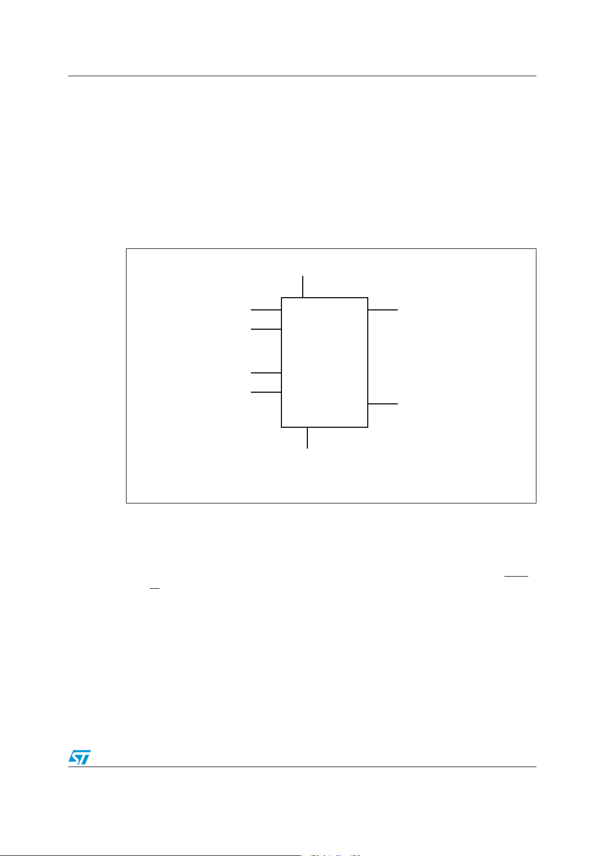
The M24LR16E-R also features an energy harvesting analog output, as well as a userconfigurable digital output pin toggling during either RF write in progress or RF busy mode.
Figure 1. Logic diagram
2
C interface and can be operated from a VCC power supply. It is
2
C mode and as 512 × 32 bits in the ISO
V
CC
SCL
Vout
SDA
AC0
M24LR16E-R
AC1
RF WIP/
#64:
V
SS
MS19740V1
2
I
C uses a two-wire serial interface, comprising a bidirectional data line and a clock line. The
devices carry a built-in 4-bit device type identifier code (1010) in accordance with the I
bus definition.
The device behaves as a slave in the I
by the serial clock. Read and Write operations are initiated by a Start condition, generated
by the bus master. The Start condition is followed by a device select code and Read/Write
bit (RW
When writing data to the memory, the device inserts an acknowledge bit during the 9
time, following the bus master’s 8-bit transmission. When data is read by the bus master, the
bus master acknowledges the receipt of the data byte in the same way. Data transfers are
terminated by a Stop condition after an Ack for Write, and after a NoAck for Read.
In the ISO15693/ISO18000-3 mode 1 RF mode, the M24LR16E-R is accessed via the
13.56 MHz carrier electromagnetic wave on which incoming data are demodulated from the
received signal amplitude modulation (ASK: amplitude shift keying). When connected to an
antenna, the operating power is derived from the RF energy and no external power supply is
required. The received ASK wave is 10% or 100% modulated with a data rate of 1.6 Kbit/s
) (as described in Ta bl e 2 ), terminated by an acknowledge bit.
2
C protocol, with all memory operations synchronized
th
2
C
bit
Doc ID 018932 Rev 8 13/143
Page 14
Description M24LR16E-R
SDAV
SS
SCL
RF WIP/BUSYAC0
Vout V
CC
MS19742V1
1
2
3
4
8
7
6
5
AC1
using the 1/256 pulse coding mode or a data rate of 26 Kbit/s using the 1/4 pulse coding
mode.
Outgoing data are generated by the M24LR16E-R load variation using Manchester coding
with one or two subcarrier frequencies at 423 kHz and 484 kHz. Data are transferred from
the M24LR16E-R at 6.6 Kbit/s in low data rate mode and 26 Kbit/s high data rate mode. The
M24LR16E-R supports the 53 Kbit/s fast mode in high data rate mode using one subcarrier
frequency at 423 kHz.
The M24LR16E-R follows the ISO 15693 and ISO 18000-3 mode 1 recommendation for
radio-frequency power and signal interface.
The M24LR16E-R provides an Energy harvesting mode on the analog output pin Vout.
When the Energy harvesting mode is activated, the M24LR16E-R can output the excess
energy coming from the RF field on the Vout analog pin. In case the RF field strength is
insufficient or when Energy harvesting mode is disabled, the analog output pin Vout goes
into high-Z state and Energy harvesting mode is automatically stopped.
The M24LR16E-R features a user configurable digital out pin RF WIP/BUSY that can be
used to drive a micro controller interrupt input pin (available only when the M24LR16E-R is
correctly powered on the Vcc pin).
When configured in the RF write in progress mode (RF WIP mode), the RF WIP/BUSY pin is
driven low for the entire duration of the RF internal write operation. When configured in the
RF busy mode (RF BUSY mode), the RF WIP/BUSY pin is driven low for the entire duration
of the RF command progress.
The RF WIP/BUSY pin is an open drain output and must be connected to a pull-up resistor.
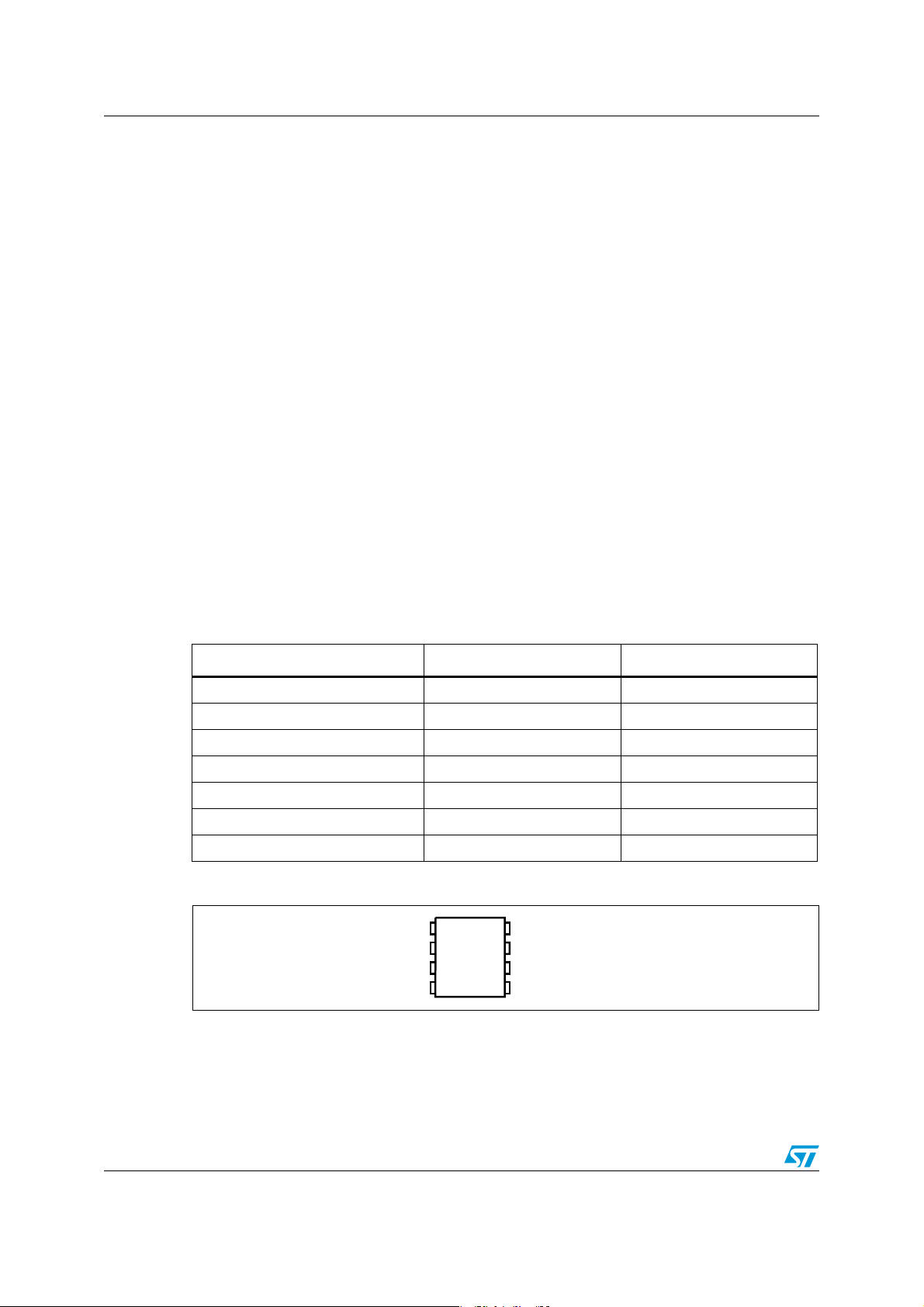
Table 1. Signal names
Signal name Function Direction
Vout Energy harvesting Output Analog output
SDA Serial Data I/O
SCL Serial Clock Input
AC0, AC1 Antenna coils I/O
V
CC
RF WIP/BUSY Digital signal Digital output
V
SS
Supply voltage
Ground
Figure 2. 8-pin package connections
1. See Section 30 for package dimensions, and how to identify pin-1.
14/143 Doc ID 018932 Rev 8
Page 15

M24LR16E-R Signal descriptions
2 Signal descriptions
2.1 Serial clock (SCL)
This input signal is used to strobe all data in and out of the device. In applications where this
signal is used by slave devices to synchronize the bus to a slower clock, the bus master
must have an open drain output, and a pull-up resistor must be connected from Serial Clock
(SCL) to V
most applications, though, this method of synchronization is not employed, and so the pullup resistor is not necessary, provided that the bus master has a push-pull (rather than open
drain) output.
2.2 Serial data (SDA)
This bidirectional signal is used to transfer data in or out of the device. It is an open drain
output that may be wire-OR’ed with other open drain or open collector signals on the bus. A
pull up resistor must be connected from Serial Data (SDA) to V
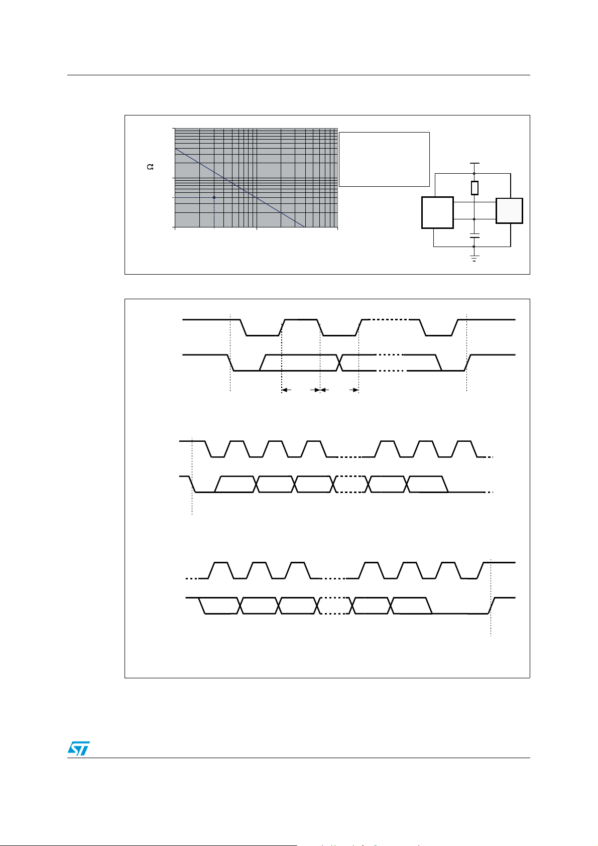
the value of the pull-up resistor can be calculated).
. (Figure 3 indicates how the value of the pull-up resistor can be calculated). In
CC
. (Figure 3 indicates how
CC
2.3 RF Write in progress / RF Busy (RF WIP/BUSY)
This configurable output signal is used either to indicate that the M24LR16E-R is executing
an internal write cycle from the RF channel or that an RF command is in progress. RF WIP
and signals are available only when the M24LR16E-R is powered by the Vcc pin. It is an
open drain output and a pull up resistor must be connected from RF WIP/BUSY to V
2.4 Energy harvesting analog output (Vout)
This analog output pin is used to deliver the analog voltage Vout available when the Energy
harvesting mode is enabled and the RF field strength is sufficient. When the Energy
harvesting mode is disabled or the RF field strength is not sufficient, the energy harvesting
analog voltage output Vout is in High-Z state.
2.5 Antenna coil (AC0, AC1)
These inputs are used to connect the device to an external coil exclusively. It is advised not
to connect any other DC or AC path to AC0 or AC1.
When correctly tuned, the coil is used to power and access the device using the ISO 15693
and ISO 18000-3 mode 1 protocols.
2.5.1 Device reset in RF mode
CC
.
To ensure a proper reset of the RF circuitry, the RF field must be turned off (100%
modulation) for a minimum t
RF_OFF
period of time.
Doc ID 018932 Rev 8 15/143
Page 16

Signal descriptions M24LR16E-R
2.6 VSS ground
VSS is the reference for the VCC supply voltage and Vout analog output voltage.
2.7 Supply voltage (VCC)
This pin can be connected to an external DC supply voltage.
Note: An internal voltage regulator allows the external voltage applied on V
M24LR16E-R, while preventing the internal power supply (rectified RF waveforms) to output
a DC voltage on the V
2.7.1 Operating supply voltage V
CC
pin.
CC
Prior to selecting the memory and issuing instructions to it, a valid and stable VCC voltage
within the specified [V
(min), VCC(max)] range must be applied (see Tab l e 1 19 ). To
CC
maintain a stable DC supply voltage, it is recommended to decouple the V
suitable capacitor (usually of the order of 10 nF) close to the V
CC/VSS
This voltage must remain stable and valid until the end of the transmission of the instruction
and, for a Write instruction, until the completion of the internal I²C write cycle (t
2.7.2 Power-up conditions
When the power supply is turned on, VCC rises from VSS to VCC. The VCC rise time must not
vary faster than 1V/µs.
2.7.3 Device reset in I²C mode
In order to prevent inadvertent write operations during power-up, a power-on reset (POR)
circuit is included. At power-up (continuous rise of V
I²C instruction until V
lower than the minimum V
has reached the power-on reset threshold voltage (this threshold is
CC
operating voltage defined in Ta bl e 1 19 ). When VCC passes
CC
over the POR threshold, the device is reset and enters the Standby power mode. However,
the device must not be accessed until V
within the specified [V
(min), VCC(max)] range.
CC
has reached a valid and stable VCC voltage
CC
In a similar way, during power-down (continuous decrease in V
below the power-on reset threshold voltage, the device stops responding to any instruction
sent to it.
), the device does not respond to any
CC
), as soon as VCC drops
CC
to supply the
CC
line with a
CC
package pins.
).
W
2.7.4 Power-down conditions
During power-down (continuous decay of VCC), the device must be in Standby power mode
(mode reached after decoding a Stop condition, assuming that there is no internal write
cycle in progress).
16/143 Doc ID 018932 Rev 8
Page 17
M24LR16E-R Signal descriptions
1
10
100
10 100 1000
Bus line capacitor (pF)
Bus line pull-up resistor
(k
)
When t
LOW
= 1.3 µs (min value for
f
C
= 400 kHz), the R
bus
× C
bus
time constant must be below the
400 ns time constant line
represented on the left.
I²C bus
master
M24xxx
R
bus
V
CC
C
bus
SCL
SDA
ai14796b
R
bus
× C
bus
= 400 ns
Here R
bus
× C
bus
= 120 ns
4 kΩ
30 pF
SCL
SDA
SCL
SDA
SDA
Start
Condition
SDA
Input
SDA
Change
AI00792B
Stop
Condition
1 23 7 89
MSB
ACK
Start
Condition
SCL
1 23 7 89
MSB ACK
Stop
Condition
Figure 3. I2C Fast mode (fC = 400 kHz): maximum R
Figure 4. I
capacitance (C
2
C bus protocol
bus
)
value versus bus parasitic
bus
Doc ID 018932 Rev 8 17/143
Page 18
Signal descriptions M24LR16E-R
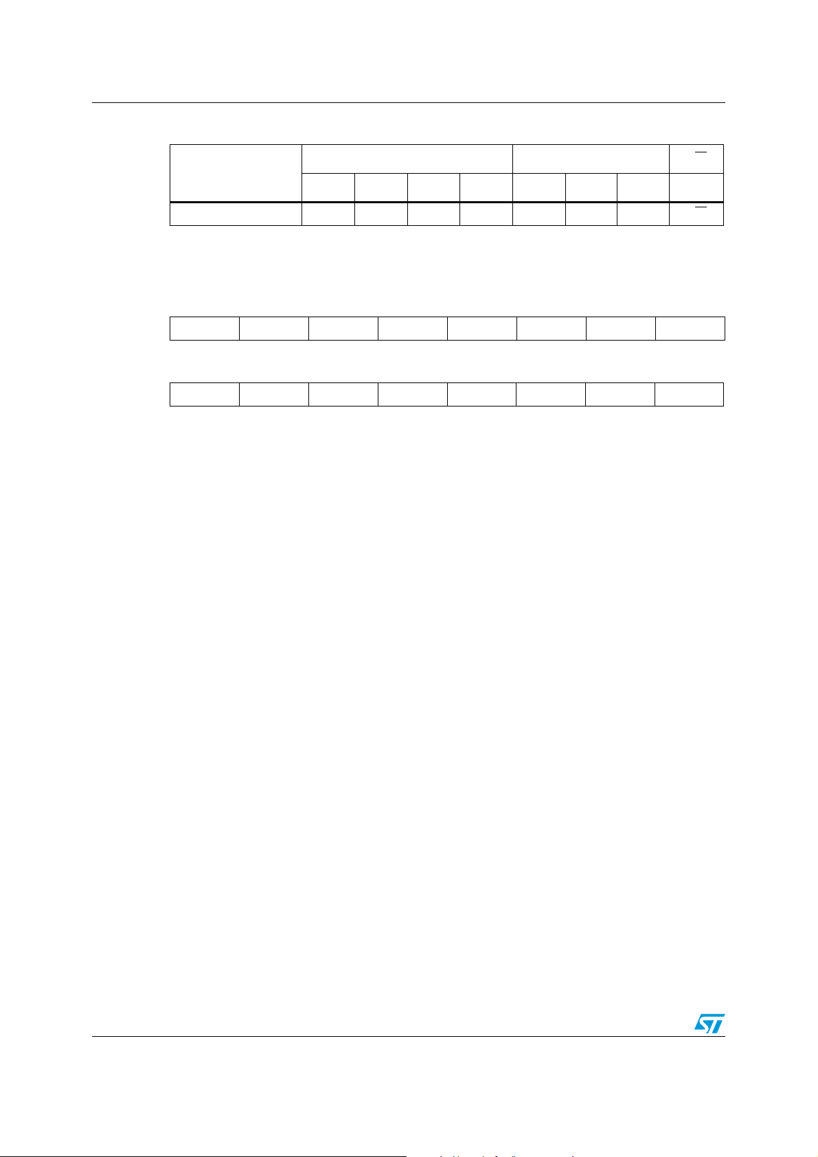
Table 2. Device select code
Device type identifier
b7 b6 b5 b4 b3 b2 b1 b0
Device select code1010E2
1. The most significant bit, b7, is sent first.
2. E2 is not connected to any external pin. It is however used to address the M24LR16E-R as described in
Section 3 and Section 4.
Table 3. Address most significant byte
b15 b14 b13 b12 b11 b10 b9 b8
Table 4. Address least significant byte
b7 b6 b5 b4 b3 b2 b1 b0
(1)
Chip Enable address RW
(2)
11RW
18/143 Doc ID 018932 Rev 8
Page 19
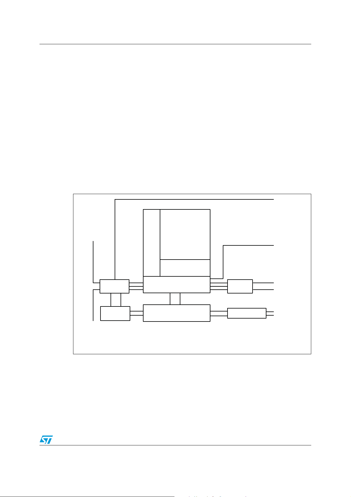
M24LR16E-R User memory organization
MS19780V1
RF V
CC
AC0
AC1
RF
Power management
Vout
RF WIP/BUSY
Logic
EEPROM
Latch
I
2
C
Contact V
CC
SCL
SDA
V
CC
V
SS
Row decoder
3 User memory organization
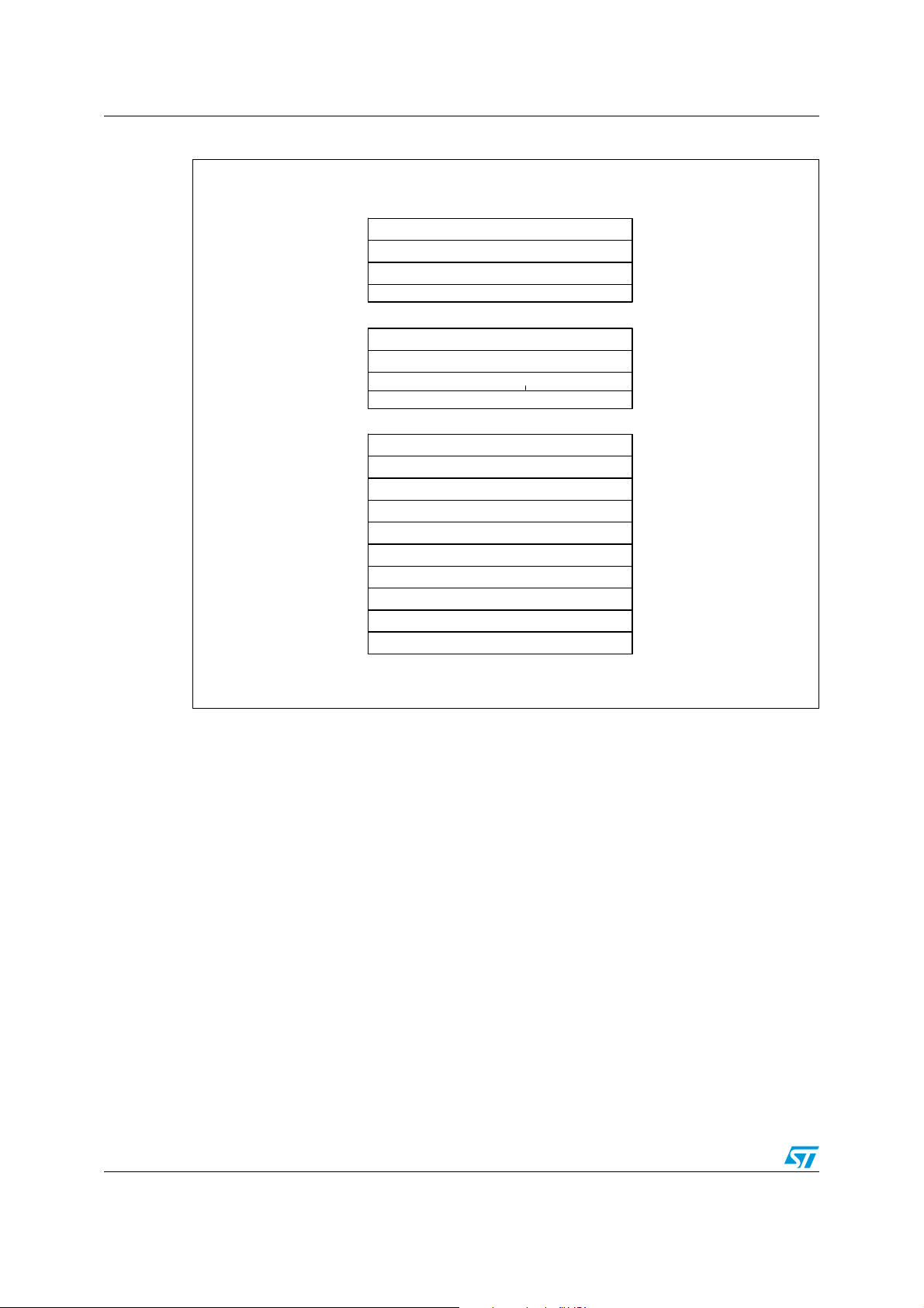
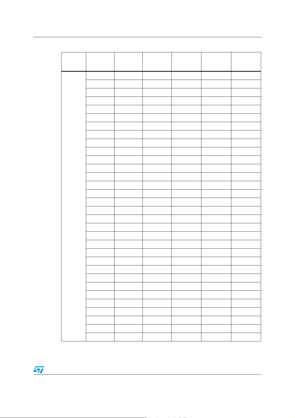
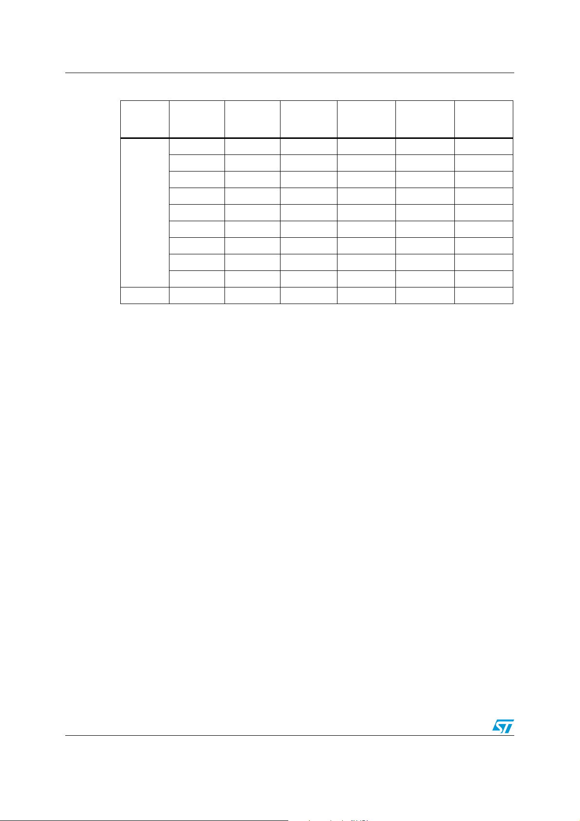
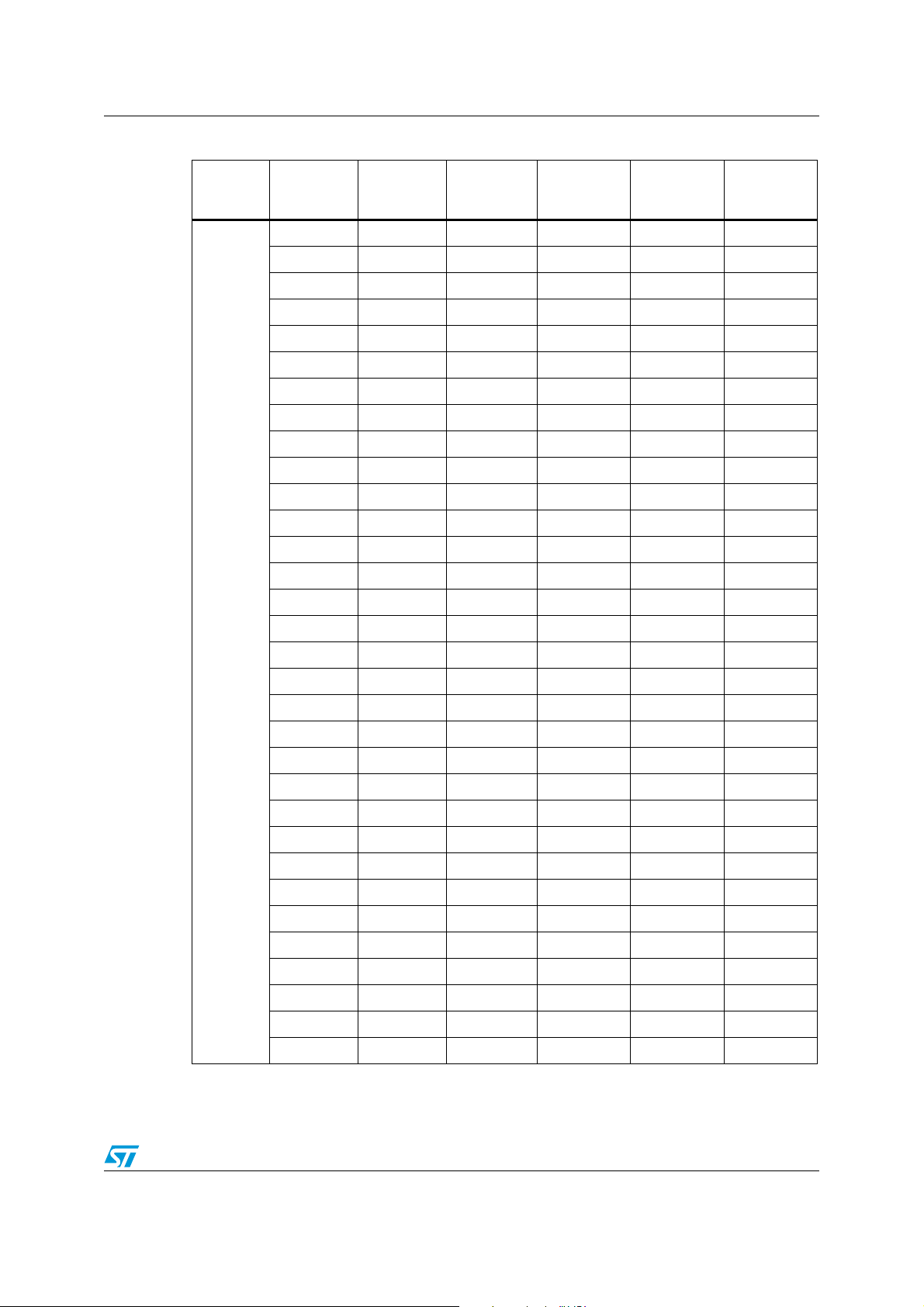
The M24LR16E-R is divided into 16 sectors of 32 blocks of 32 bits, as shown in Ta bl e 5 .
Figure 6 shows the memory sector organization. Each sector can be individually read-
and/or write-protected using a specific password command. Read and write operations are
possible if the addressed data are not in a protected sector.
The M24LR16E-R also has a 64-bit block that is used to store the 64-bit unique identifier
(UID). The UID is compliant with the ISO 15963 description, and its value is used during the
anticollision sequence (Inventory). This block is not accessible by the user and its value is
written by ST on the production line.
The M24LR16E-R includes an AFI register that stores the application family identifier, and a
DSFID register that stores the data storage family identifier used in the anticollision
algorithm.
The M24LR16E-R has four 32-bit blocks that store an I
codes.
Figure 5. Circuit diagram
2
C password plus three RF password
Doc ID 018932 Rev 8 19/143
Page 20
User memory organization M24LR16E-R
MS19741V1
1 Kbit EEPROM sector
1 Kbit EEPROM sector
1 Kbit EEPROM sector
1 Kbit EEPROM sector
Sector
Area
Sector security
status
1 Kbit EEPROM sector
1 Kbit EEPROM sector
1 Kbit EEPROM sector
1 Kbit EEPROM sector
I²C password
RF password 1
RF password 2
RF password 3
8-bit DSFID
8-bit AFI
8-bit configuration
16-bit I²C Write Lock_bit
64-bit UID
0
1
2
3
12
13
14
15
5 bits
5 bits
5 bits
5 bits
5 bits
5 bits
5 bits
5 bits
System
System
System
System
System
System
System
System
80-bit SSS
System
Figure 6. Memory sector organization
Sector details
The M24LR16E-R user memory is divided into 16 sectors. Each sector contains 1024 bits.
20/143 Doc ID 018932 Rev 8
The protection scheme is described in Section 4: System memory area.
In RF mode, a sector provides 32 blocks of 32 bits. Each read and write access is done by
block. Read and write block accesses are controlled by a Sector Security Status byte that
defines the access rights to the 32 blocks contained in the sector. If the sector is not
protected, a Write command updates the complete 32 bits of the selected block.
2
In I
C mode, a sector provides 128 bytes that can be individually accessed in Read and
Write modes. When protected by the corresponding I2C_Write_Lock bit, the entire sector is
write-protected. To access the user memory, the device select code used for any I
command must have the E2 Chip Enable address at 0.
2
C
Page 21
M24LR16E-R User memory organization
Table 5. Sector details
Sector
number
0
RF block
address
I2C byte
address
Bits [31:24] Bits [23:16] Bits [15:8] Bits [7:0]
0 0 user user user user
1 4 user user user user
2 8 user user user user
3 12 user user user user
4 16 user user user user
5 20 user user user user
6 24 user user user user
7 28 user user user user
8 32 user user user user
9 36 user user user user
10 40 user user user user
11 44 user user user user
12 48 user user user user
13 52 user user user user
14 56 user user user user
15 60 user user user user
16 64 user user user user
17 68 user user user user
18 72 user user user user
19 76 user user user user
20 80 user user user user
21 84 user user user user
22 88 user user user user
23 92 user user user user
24 96 user user user user
25 100 user user user user
26 104 user user user user
27 108 user user user user
28 112 user user user user
29 116 user user user user
30 120 user user user user
31 124 user user user user
Doc ID 018932 Rev 8 21/143
Page 22
User memory organization M24LR16E-R
Table 5. Sector details (continued)
Sector
number
1
... ... ... ... ... ... ...
RF block
address
32 128 user user user user
33 132 user user user user
34 136 user user user user
35 140 user user user user
36 144 user user user user
37 148 user user user user
38 152 user user user user
39 156 user user user user
... ... ... ... ... ...
I2C byte
address
Bits [31:24] Bits [23:16] Bits [15:8] Bits [7:0]
22/143 Doc ID 018932 Rev 8
Page 23
M24LR16E-R User memory organization
Table 5. Sector details (continued)
Sector
number
15
RF block
address
480 1920 user user user user
481 1924 user user user user
482 1928 user user user user
483 1932 user user user user
484 1936 user user user user
485 1940 user user user user
486 1944 user user user user
487 1948 user user user user
488 1952 user user user user
489 1956 user user user user
490 1960 user user user user
491 1964 user user user user
492 1968 user user user user
493 1972 user user user user
494 1976 user user user user
495 1980 user user user user
496 1984 user user user user
I2C byte
address
Bits [31:24] Bits [23:16] Bits [15:8] Bits [7:0]
497 1988 user user user user
498 1992 user user user user
499 1996 user user user user
500 2000 user user user user
501 2004 user user user user
502 2008 user user user user
503 2012 user user user user
504 2016 user user user user
505 2020 user user user user
506 2024 user user user user
507 2028 user user user user
508 2032 user user user user
509 2036 user user user user
510 2040 user user user user
511 2044 user user user user
Doc ID 018932 Rev 8 23/143
Page 24
System memory area M24LR16E-R
4 System memory area
4.1 M24LR16E-R block security in RF mode
The M24LR16E-R provides a special protection mechanism based on passwords. In RF
mode, each memory sector of the M24LR16E-R can be individually protected by one out of
three available passwords, and each sector can also have Read/Write access conditions
set.
Each memory sector of the M24LR16E-R is assigned with a Sector security status byte
including a Sector Lock bit, two Password Control bits and two Read/Write protection bits,
as shown in Ta bl e 7 .
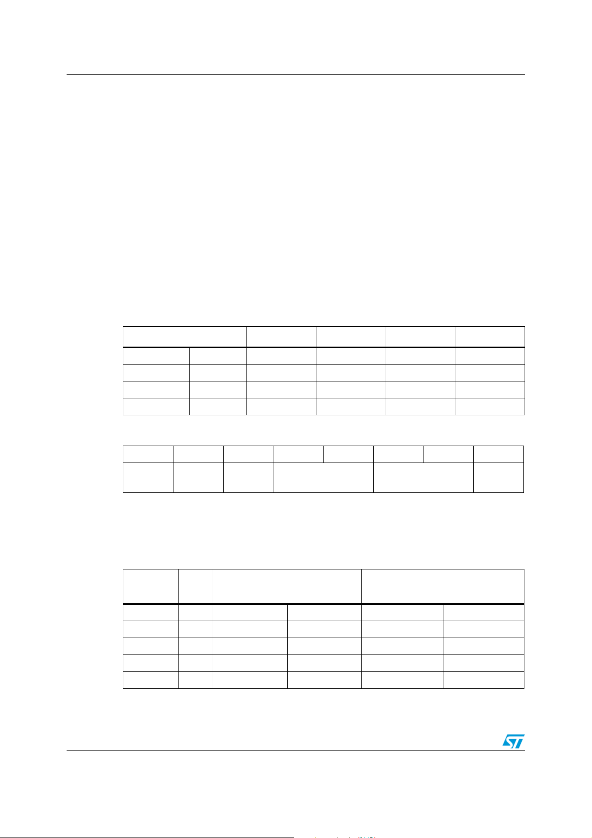
Ta bl e 6 describes the organization of the Sector security status byte, which can be read
using the Read Single Block and Read Multiple Block commands with the Option_flag set
to 1.
On delivery, the default value of the SSS bytes is set to 00h.
Table 6. Sector security status byte area
I2C byte address Bits [31:24] Bits [23:16] Bits [15:8] Bits [7:0]
E2 = 1 0 SSS 3 SSS 2 SSS 1 SSS 0
E2 = 1 4 SSS 7 SSS 6 SSS 5 SSS 4
E2 = 1 8 SSS 11 SSS 10 SSS 9 SSS 8
E2 = 1 12 SSS 15 SSS 14 SSS 13 SSS 12
Table 7. Sector security status byte organization
b
7
0 0 0 Password control bits
b
6
b
5
b
4
b
3
b
2
Read / Write
protection bits
b
1
b
0
Sector
Lock
When the Sector Lock bit is set to 1, for instance by issuing a Lock-sector command, the two
Read/Write protection bits (b
, b2) are used to set the Read/Write access of the sector as
1
described in Ta b le 8 .
Table 8. Read / Write protection bit setting
Sector
Lock
, b
b
2
1
Sector access
when password presented
when password not presented
0 xx Read Write Read Write
1 00 Read Write Read No Write
1 01 Read Write Read Write
Sector access
1 10 Read Write No Read No Write
1 11 Read No Write No Read No Write
24/143 Doc ID 018932 Rev 8
Page 25
M24LR16E-R System memory area
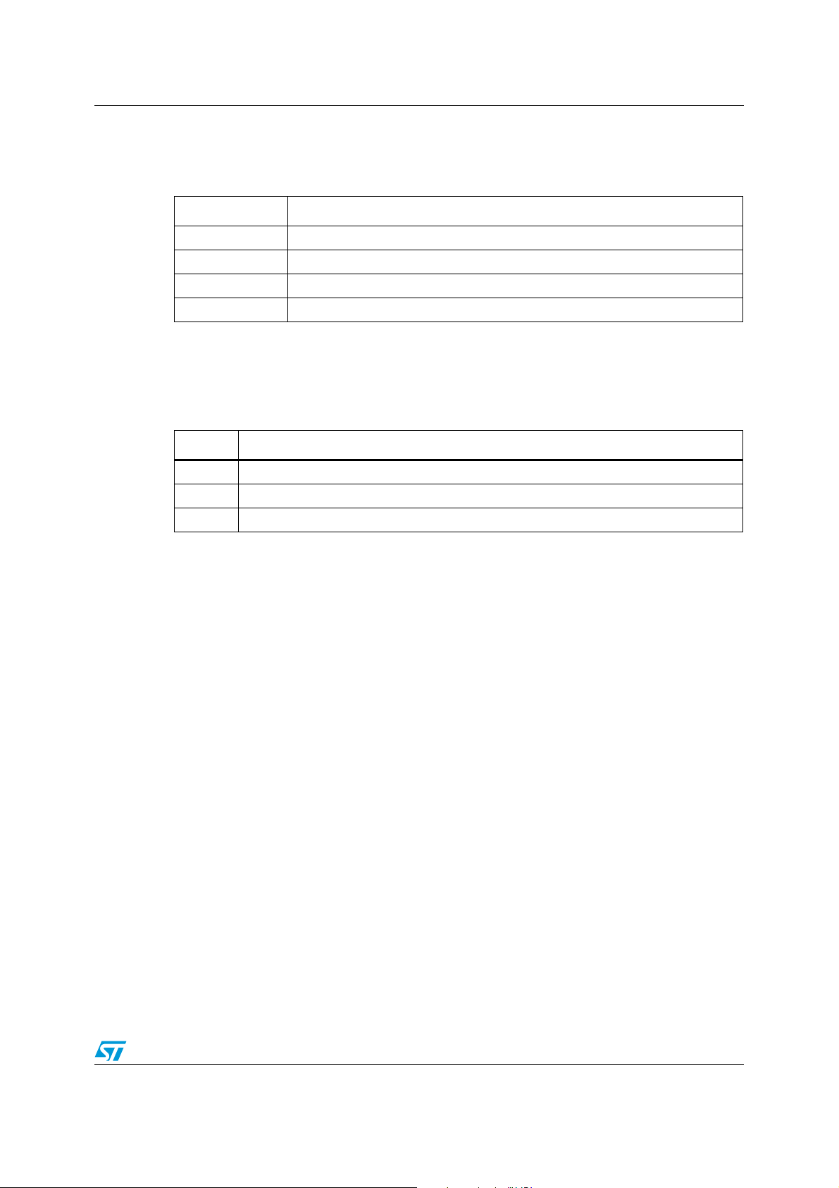
The next two bits of the Sector security status byte (b3, b4) are the password control bits.
The value of these two bits is used to link a password to the sector, as defined in Ta bl e 9 .
Table 9. Password control bits
b4, b
3
00 The sector is not protected by a password.
01 The sector is protected by password 1.
10 The sector is protected by password 2.
11 The sector is protected by password 3.
Password
The M24LR16E-R password protection is organized around a dedicated set of commands,
plus a system area of three password blocks where the password values are stored. This
system area is described in Ta bl e 1 0.
Table 10. Password system area
Add
1 Password 1
2 Password 2
3 Password 3
The dedicated commands for protection in RF mode are:
● Write-sector password:
The Write-sector password command is used to write a 32-bit block into the password
system area. This command must be used to update password values. After the write
cycle, the new password value is automatically activated. It is possible to modify a
password value after issuing a valid Present-sector password command. On delivery,
the three default password values are set to 0000 0000h and are activated.
● Lock-sector:
The Lock-sector command is used to set the sector security status byte of the selected
sector. Bits b
command. The sector lock bit, b
to b1 of the sector security status byte are affected by the Lock-sector
4
, is set to 1 automatically. After issuing a Lock-sector
0
command, the protection settings of the selected sector are activated. The protection of
a locked block cannot be changed in RF mode. A Lock-sector command sent to a
locked sector returns an error code.
Doc ID 018932 Rev 8 25/143
Page 26
System memory area M24LR16E-R
● Present-sector password:
The Present-sector password command is used to present one of the three passwords
to the M24LR16E-R in order to modify the access rights of all the memory sectors
linked to that password (Ta b le 8 ) including the password itself. If the presented
password is correct, the access rights remain activated until the tag is powered off or
until a new Present-sector password command is issued. If the presented password
value is not correct, all the access rights of all the memory sectors are deactivated.
● Sector security status byte area access conditions in I2C mode:
2
In I
C mode, read access to the sector security status byte area is always allowed.
Write access depends on the correct presentation of the I
2
C password (see
Section 5.16.1: I2C present password command description).
To access the Sector security status byte area, the device select code used for any I
2
C
command must have the E2 Chip Enable address at 1.
2
An I
C write access to a sector security status byte re-initializes the RF access
condition to the given memory sector.
4.1.1 Example of the M24LR16E-R security protection in RF mode
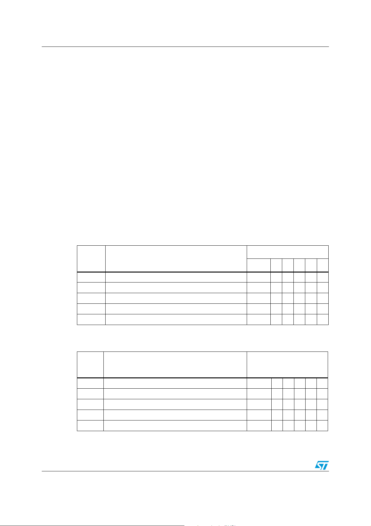
Ta bl e 1 1 and Ta bl e 1 2 show the sector security protections before and after a valid Present-
sector password command. Tab le 1 1 shows the sector access rights of an M24LR16E-R
after power-up. After a valid Present-sector password command with password 1, the
memory sector access is changed as shown in Ta bl e 1 2.
Table 11. M24LR16E-R sector security protection after power-up
Sector
address
0 Protection: standard Read No Write xxx 00001
1 Protection: pswd 1 Read No Write xxx 01001
2 Protection: pswd 1 Read Write xxx 01011
3 Protection: pswd 1 No Read No Write xxx 01101
4 Protection: pswd 1 No Read No Write xxx 01111
Table 12. M24LR16E-R sector security protection after a valid presentation of
Sector security status byte
b
7b6b5b4b3b2b1b0
password 1
Sector
address
0 Protection: standard Read No Write xxx 0 0 0 0 1
1 Protection: pswd 1 Read Write xxx 0 1 0 0 1
2 Protection: pswd 1 Read Write xxx 0 1 0 1 1
3 Protection: pswd 1 Read Write xxx 0 1 1 0 1
4 Protection: pswd 1 Read No Write xxx 0 1 1 1 1
Sector security status byte
b7b6b5b4b3b2b1b
0
26/143 Doc ID 018932 Rev 8
Page 27
M24LR16E-R System memory area
4.2 M24LR16E-R block security in I²C mode (I2C_Write_Lock bit area)
In the I2C mode only, it is possible to protect individual sectors against Write operations.
This feature is controlled by the I2C_Write_Lock bits stored in the 2 bytes of the
I2C_Write_Lock bit area. I2C_Write_Lock bit area starts from location 2048 (see Ta bl e 1 3 ).
To access the I2C_Write_Lock bit area, the device select code used for any I
must have the E2 Chip Enable address at 1.
2
C command
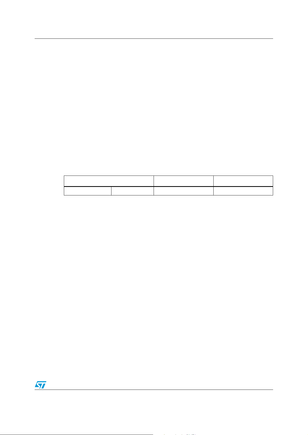
Using these 16 bits, it is possible to write-protect all the 16 sectors of the M24LR16E-R
memory. Each bit controls the I
is always possible to unprotect a sector in the I
2
C write access to a specific sector as shown in Ta bl e 1 3 . It
2
C mode. When an I2C_Write_Lock bit is
reset to 0, the corresponding sector is unprotected. When the bit is set to 1, the
corresponding sector is write-protected.
2
In I
C mode, read access to the I2C_Write_Lock bit area is always allowed. Write access
depends on the correct presentation of the I
2
C password.
On delivery, the default value of the eight bytes of the I2C_Write_Lock bit area is reset to
00h.
m
Table 13. I2C_Write_Lock bit
I2C byte address Bits [15:8] Bits [7:0]
E2 = 1 2048 sectors 15-8 sectors 7-0
4.3 Configuration byte and Control register
The M24LR16E-R offers an 8-bit non-volatile Configuration byte located at I²C location 2320
of the system area used to store the RF WIP/BUSY pin and the energy harvesting
configuration (see Ta b le 1 4 ).
The M24LR16E-R also offers an 8-bit volatile Control register located at I²C location 2336 of
the system area used to store the energy harvesting enable bit as well as a FIELD_ON bit
indicator (see Tab le 1 5 ).
4.3.1 RF WIP/BUSY pin configuration
The M24LR16E-R features a configurable open drain output RF WIP/BUSY pin used to
provide RF activity information to an external device.
The RF WIP/BUSY pin functionality depends on the value of bit 3 of the Configuration byte.
● RF busy mode
When bit 3 of the Configuration byte is set to 0, the RF WIP/BUSY pin is configured in RF
busy mode.
The purpose of this mode is to indicate to the I²C bus master whether the M24LR16E-R is
busy in RF mode or not.
In this mode, the RF WIP/BUSY pin is tied to 0 from the RF command Start Of Frame (SOF)
until the end of the command execution.
Doc ID 018932 Rev 8 27/143
Page 28

System memory area M24LR16E-R
If a bad RF command is received, the RF WIP/BUSY pin is tied to 0 from the RF command
SOF until the reception of the RF command CRC. Otherwise, the RF WIP/BUSY pin is in
high-Z state.
When tied to 0, the RF WIP/BUSY signal returns to High-Z state if the RF field is cut-off.
During execution of I²C commands, the RF WIP/BUSY pin remains in high-Z state.
● RF Write in progress
When bit 3 of the Configuration byte is set to 1, the RF WIP/BUSY pin is configured in RF
Write in progress mode.
The purpose of this mode is to indicate to the I²C bus master that some data have been
changed in RF mode.
In this mode, the RF WIP/BUSY pin is tied to 0 for the duration of an internal write operation
(i.e. between the end of a valid RF write command and the beginning of the RF answer).
During execution of I²C write operations, the RF WIP/BUSY pin remains in high-Z state.
4.3.2 Energy harvesting configuration
The M24LR16E-R features an Energy harvesting mode on the Vout analog output.
The general purpose of the Energy harvesting mode is to deliver a part of the non-
necessary RF power received by the M24LR16E-R on the AC0-AC1 RF input in order to
supply an external device. The current consumption on the analog voltage output Vout is
limited to ensure that the M24LR16E-R is correctly supplied during the powering of the
external device.
When the Energy harvesting mode is enabled and the power delivered on the AC0-AC1 RF
input exceeds the minimum required P
AC0-AC1_min
, the M24LR16E-R is able to deliver a
limited and unregulated voltage on the Vout pin, assuming the current consumption on the
Vout does not exceed the I
sink_max
maximum value.
If one of the condition above is not met, the analog voltage output pin Vout is set in High-Z
state.
For robust applications using the Energy harvesting mode, four current fan-out levels can be
chosen.
● Vout sink current configuration
The sink current level is chosen by programming EH_cfg1 and EH_cfg0 into the
Configuration byte (see Ta bl e 1 4 ).
The minimum power level required on AC0-AC1 RF input P
voltage Vout, as well as the maximum current consumption I
AC0-AC1_min
sink_max
, the delivered
on the Vout pin
corresponding to the <EH_cfg1,EH_cfg0> bit values are described in Ta bl e 1 26 .
Table 14. Configuration byte
I2C byte address Bit 7 Bit 6 Bit 5 Bit 4 Bit 3 Bit 2 BIT 1 BIT 0
(1)
E2=1 2320 X
1. Bit 7 to Bit 4 are don’t care bits.
(1)X(1)X(1)
X
RF WIP/BUSY EH_mode EH_cfg1 EH_cfg0
28/143 Doc ID 018932 Rev 8
Page 29
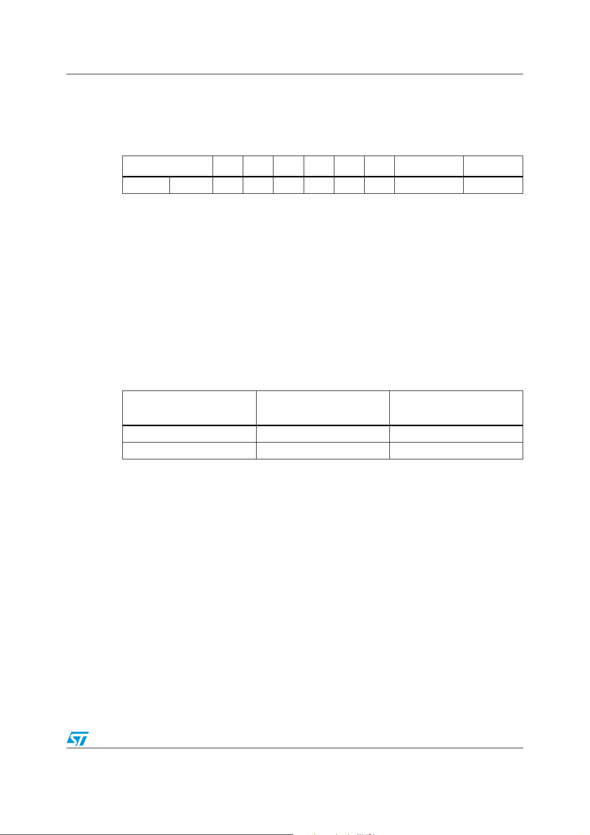
M24LR16E-R System memory area
● Energy harvesting enable control
Delivery of Energy harvesting analog output voltage on the Vout pin depends on the value of
the EH_enable bit of the volatile Control register (see Tab le 1 5 ).
Table 15. Control register
I2C byte address Bit 7 Bit 6 Bit 5 Bit 4 Bit 3 Bit 2 BIT 1 BIT 0
E2=1 2336 0
1. Bit 7 to Bit 1 are read-only bits.
(1)
(1)
0
(1)
0
(1)
0
(1)
0
(1)
0
FIELD_ON
(1)
EH_enable
– When set to 1, the EH_enable bit enables the Energy harvesting mode, meaning
that the Vout analog output signal is delivered when the P
AC0-AC1_min
and I
sink_max
conditions corresponding to the chosen sink current configuration bit are met (see
Ta bl e 1 26 ).
– When set to 0, the EH_enable bit disable the Energy harvesting mode and the
analog output Vout remains in set in High-Z state.
● Energy harvesting default mode control
At power-up, in I²C or RF mode, the EH_enable bit is updated according to the value of the
EH_mode bit stored in the non-volatile Configuration byte (see Ta bl e 1 6 ). In other words, the
EH_mode bit is used to configure whether the Energy harvesting mode is enabled or not by
default.
Table 16. EH_enable bit value after power-up
EH_mode value EH_enable after power-up
Energy harvesting
after power-up
0 1 enabled
1 0 disabled
4.3.3 FIELD_ON indicator bit
The FIELD_ON bit indicator located as Bit 1 of the Control register is a read-only bit used to
indicate when the RF power level delivered to the M24LR16E-R is sufficient to execute RF
commands.
● When FIELD_ON = 0, the M24LR16E-R is not able to execute any RF commands.
● When FIELD_ON =1, the M24LR16E-R is able to execute any RF commands.
Note: During read access to the Control register in RF mode, the FIELD_ON bit is always read
at 1.
Doc ID 018932 Rev 8 29/143
Page 30

System memory area M24LR16E-R
4.3.4 Configuration byte access in I²C and RF modes
In I²C mode, read and write accesses to the non-volatile Configuration byte are always
allowed. To access the Configuration byte, the device select code used for any I²C
command must have the E2 Chip enable address at 1.
The dedicated commands to access the Configuration byte in RF mode are:
● Read configuration byte command (ReadCfg):
The ReadCfg command is used to read the eight bits of the Configuration byte.
● Write energy harvesting configuration command (WriteEHCfg):
The WriteEHCfg command is used to write the EH_mode, EH_cfg1 and EH_cfg0 bits into
the Configuration byte.
● Write RF WIP/BUSY pin configuration command (WriteDOCfg):
The WriteDOCfg command is used to write the RF WIP/BUSY bit into the Configuration
byte.
After any write access to the Configuration byte, the new configuration is automatically
applied.
4.3.5 Control register access in I²C or RF mode
In I²C mode, read and write accesses to the volatile Control register are always allowed. To
access the Control register, the device select code used for any I²C command must have the
E2 Chip enable address at 1.
The dedicated commands to access the Control register in RF mode are:
● Check energy harvesting enable bit command (CheckEHEn):
The CheckEHEn command is used to read the eight bits of the Control register. When it is
run, the FIELD_ON bit is always read at 1.
● Set/reset energy harvesting enable bit command (SetRstEHEn):
The SetRstEHEn command is used to set or reset the value of the EH_enable bit into the
Control register.
4.4 ISO 15693 system parameters
The M24LR16E-R provides the system area required by the ISO 15693 RF protocol, as
shown in Ta bl e 1 7 .
The first 32-bit block starting from I
is used to activate/deactivate the write protection of the protected sector in I
power-on, all user memory sectors protected by the I2C_Write_Lock bits can be read but
cannot be modified. To remove the write protection, it is necessary to use the I
password described in Figure 12. When the password is correctly presented — that is, when
all the presented bits correspond to the stored ones — it is also possible to modify the I
password using the I2C write password command described in Figure 13.
2
C address 2304 stores the I2C password. This password
2
C mode. At
2
C present
2
C
The next three 32-bit blocks store the three RF passwords. These passwords are neither
read- nor write- accessible in the I
30/143 Doc ID 018932 Rev 8
2
C mode.
Page 31
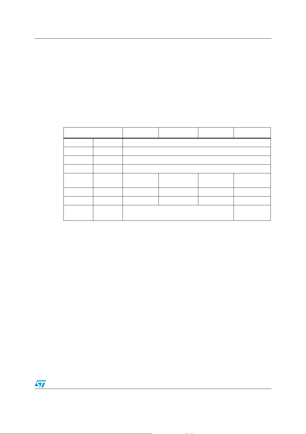
M24LR16E-R System memory area
The next byte stores the Configuration byte, at I²C location 2320. This Control register is
used to store the three energy harvesting configuration bits and the RF WIP/BUSY
configuration bit.
The next two bytes are used to store the AFI, at I
location 2323. These two values are used during the RF inventory sequence. They are readonly in the I
2
C mode.
2
C location 2322, and the DSFID, at I2C
The next eight bytes, starting from location 2324, store the 64-bit UID programmed by ST on
the production line. Bytes at I
2
C locations 2332 to 2335 store the IC Ref and the Mem_Size
data used by the RF Get_System_Info command. The UID, Mem_Size and IC ref values are
read-only data.
Table 17. System parameter sector
I2C byte address Bits [31:24] Bits [23:16] Bits [15:8] Bits [7:0]
2
E2 = 1 2304 I
C password
E2 = 1 2308 RF password 1
E2 = 1 2312 RF password 2
E2 = 1 2316 RF password 3
E2 = 1 2320 DSFID (FFh) AFI (00h) ST reserved
E2 = 1 2324 UID UID UID UID
E2 = 1 2328 UID (E0h) UID (02h) UID UID
E2 = 1 2332
1. Delivery state: I2C password= 0000 0000h, RF password = 0000 0000h, Configuration byte = F4h
Mem_Size
(03 01FFh)
(1)
(1)
(1)
(1)
Configuration
byte (F4h)
IC Ref (4Eh)
Doc ID 018932 Rev 8 31/143
Page 32

I2C device operation M24LR16E-R
5 I2C device operation
The device supports the I2C protocol. This is summarized in Figure 4. Any device that sends
data to the bus is defined as a transmitter, and any device that reads data is defined as a
receiver. The device that controls the data transfer is known as the bus master, and the
other as the slave device. A data transfer can only be initiated by the bus master, which also
provides the serial clock for synchronization. The M24LR16E-R device is a slave in all
communications.
5.1 Start condition
Start is identified by a falling edge of serial data (SDA) while the serial clock (SCL) is stable
in the high state. A Start condition must precede any data transfer command. The device
continuously monitors (except during a write cycle) the SDA and the SCL for a Start
condition, and does not respond unless one is given.
5.2 Stop condition
Stop is identified by a rising edge of serial data (SDA) while the serial clock (SCL) is stable
and driven high. A Stop condition terminates communication between the device and the
bus master. A Read command that is followed by NoAck can be followed by a Stop condition
to force the device into the Standby mode. A Stop condition at the end of a Write command
triggers the internal write cycle.
5.3 Acknowledge bit (ACK)
The acknowledge bit is used to indicate a successful byte transfer. The bus transmitter,
whether it be bus master or slave device, releases the serial data (SDA) after sending eight
bits of data. During the 9
the receipt of the eight data bits.
th
clock pulse period, the receiver pulls the SDA low to acknowledge
5.4 Data input
During data input, the device samples serial data (SDA) on the rising edge of the serial clock
(SCL). For correct device operation, the SDA must be stable during the rising edge of the
SCL, and the SDA signal must change only when the SCL is driven low.
5.5 I²C timeout
During the execution of an I²C operation, RF communications are not possible.
To prevent RF communication freezing due to inadvertent unterminated instructions sent to
the I²C bus, the M24LR16E-R features a timeout mechanism that automatically resets the
I²C logic block.
32/143 Doc ID 018932 Rev 8
Page 33
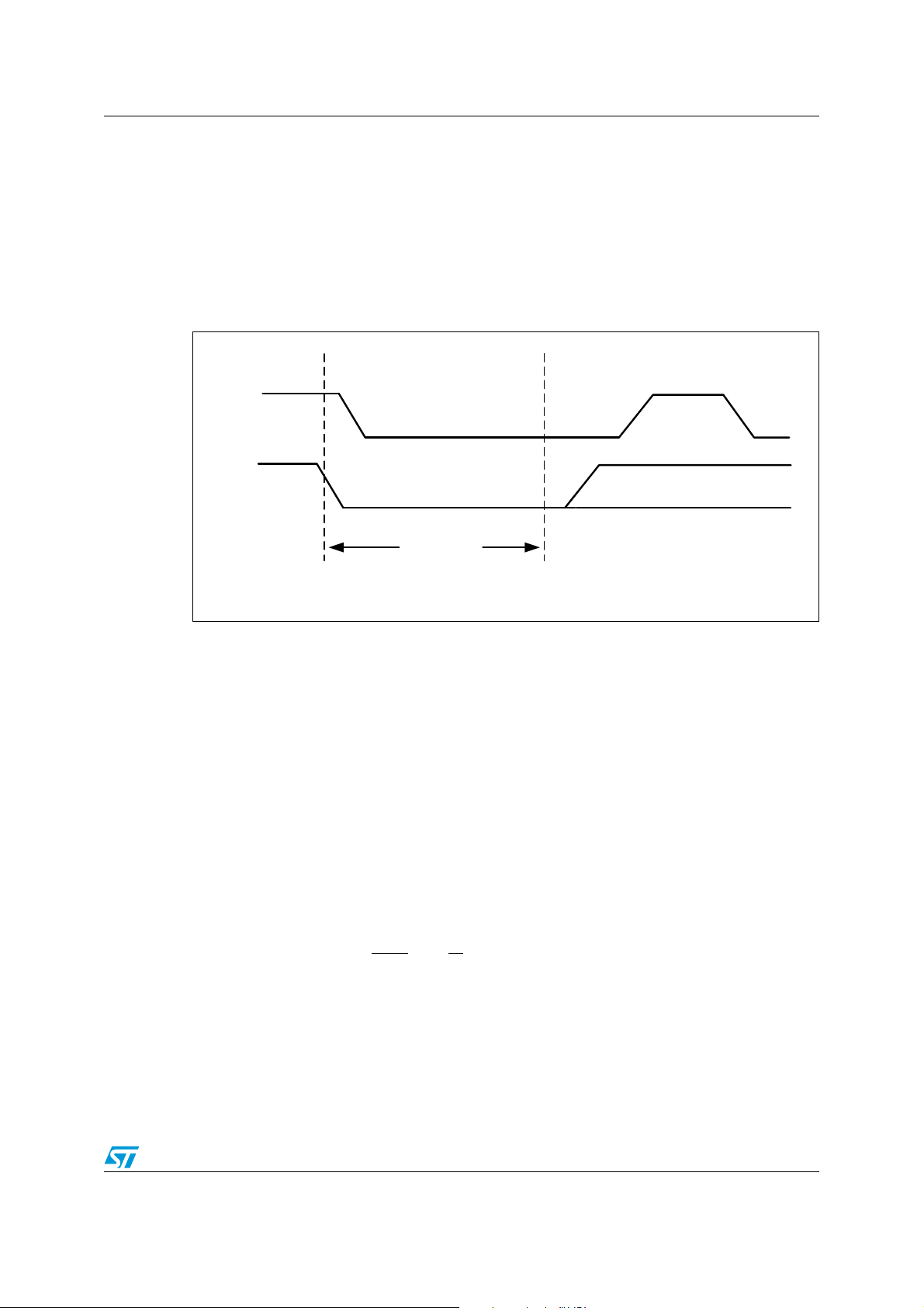
M24LR16E-R I2C device operation
MS19779V1
SCL
SDA
t
START_OUT
Start
condition
5.5.1 I²C timeout on Start condition
I²C communication with the M24LR16E-R starts with a valid Start condition, followed by a
device select code.
If the delay between the Start condition and the following rising edge of the Serial Clock
(SCL) that samples the most significant of the Device Select exceeds the t
START_OUT
(see Ta bl e 1 23 ), the I²C logic block is reset and further incoming data transfer is ignored
until the next valid Start condition.
Figure 7. I²C timeout on Start condition
time
5.5.2 I²C timeout on clock period
During data transfer on the I²C bus, the serial clock high pulse width High (t
clock pulse width Low (
t
) exceeds the maximum value specified in Ta bl e 1 2 3 , the I²C
CLCH
logic block is reset and any further incoming data transfer is ignored until the next valid Start
condition.
5.6 Memory addressing
To start communication between the bus master and the slave device, the bus master must
initiate a Start condition. Following this, the bus master sends the device select code, shown
in Ta bl e 2 (on Serial Data (SDA), most significant bit first).
The device select code consists of a 4-bit device type identifier and a 3-bit Chip Enable
“Address” (E2,1,1). To address the memory array, the 4-bit device type identifier is 1010b.
Refer to Ta bl e 2 .
The eighth bit is the Read/Write
If a match occurs on the device select code, the corresponding device gives an
acknowledgment on serial data (SDA) during the ninth bit time. If the device does not match
the device select code, it deselects itself from the bus, and goes into Standby mode.
bit (RW). It is set to 1 for Read and to 0 for Write operations.
CHCL
) or serial
Doc ID 018932 Rev 8 33/143
Page 34
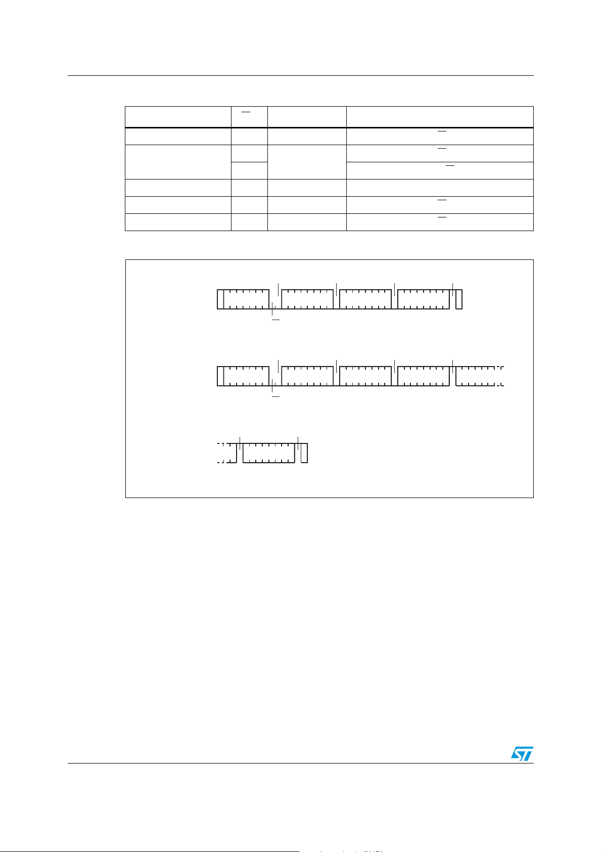
I2C device operation M24LR16E-R
Stop
Start
Byte Write Dev select Byte address Byte address Data in
Start
Page Write Dev select Byte address Byte address Data in 1
Data in 2
AI15115
Page Write
(cont'd)
Stop
Data in N
ACK ACK ACK NO ACK
R/W
ACK ACK ACK NO ACK
R/W
NO ACK NO ACK
Table 18. Operating modes
Mode RW bit Bytes Initial sequence
Current address read 1 1 Start, device select, RW
Random address read
0
1
Start, device select, RW
1 reStart, device select, RW
= 1
= 0, address
= 1
Sequential read 1 ≥ 1 Similar to current or random address read
Byte write 0 1 Start, device select, RW = 0
Page write 0 ≤ 4 bytes Start, device select, RW
= 0
Figure 8. Write mode sequences with I2C_Write_Lock bit = 1 (data write inhibited)
34/143 Doc ID 018932 Rev 8
Page 35

M24LR16E-R I2C device operation
5.7 Write operations
Following a Start condition, the bus master sends a device select code with the Read/Write
bit (RW
address bytes. The device responds to each address byte with an acknowledge bit, and
then waits for the data byte.
Writing to the memory may be inhibited if the I2C_Write_Lock bit = 1. A Write instruction
issued with the I2C_Write_Lock bit = 1 and with no I2C_Password presented does not
modify the memory contents, and the accompanying data bytes are not acknowledged, as
shown in Figure 8.
Each data byte in the memory has a 16-bit (two byte wide) address. The most significant
byte (Ta bl e 3 ) is sent first, followed by the least significant byte (Tab le 4 ). Bits b15 to b0 form
the address of the byte in memory.
When the bus master generates a Stop condition immediately after the Ack bit (in the tenthbit time slot), either at the end of a byte write or a page write, the internal write cycle is
triggered. A Stop condition at any other time slot does not trigger the internal write cycle.
) reset to 0. The device acknowledges this, as shown in Figure 8, and waits for two
After the Stop condition, the delay t
the device’s internal address counter is incremented automatically, to point to the next byte
address after the last one that was modified.
During the internal write cycle, the serial data (SDA) signal is disabled internally, and the
device does not respond to any requests.
5.8 Byte write
After the device select code and the address bytes, the bus master sends one data byte. If
the addressed location is write-protected by the I2C_Write_Lock bit (= 1), the device replies
with NoAck, and the location is not modified. If the addressed location is not write-protected,
the device replies with Ack. The bus master terminates the transfer by generating a Stop
condition, as shown in Figure 9.
5.9 Page write
The Page write mode allows up to four bytes to be written in a single write cycle, provided
that they are all located in the same “row” in the memory: that is, the most significant
memory address bits (b12-b2) are the same. If more bytes are sent than fit up to the end of
the row, a condition known as “roll-over” occurs. This should be avoided, as data starts to
become overwritten in an implementation-dependent way.
The bus master sends from one to four bytes of data, each of which is acknowledged by the
device if the I2C_Write_Lock bit = 0 or the I2C_Password was correctly presented. If the
I2C_Write_Lock_bit = 1 and the I2C_password are not presented, the contents of the
addressed memory location are not modified, and each data byte is followed by a NoAck.
After each byte is transferred, the internal byte address counter (inside the page) is
incremented. The transfer is terminated by the bus master generating a Stop condition.
, and the successful completion of a Write operation,
W
Doc ID 018932 Rev 8 35/143
Page 36
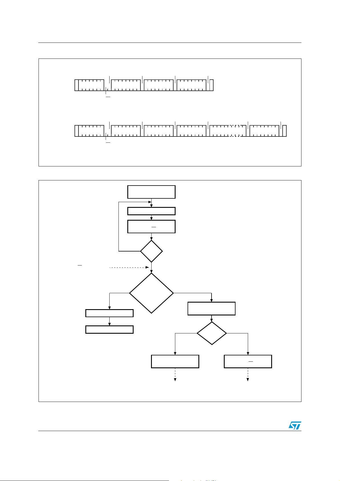
I2C device operation M24LR16E-R
Write cycle
in progress
AI01847d
Next
operation is
addressing the
memory
Start condition
Device select
with RW = 0
ACK
Returned
YES
NO
YESNO
ReStart
Stop
Data for the
Write operation
Device select
with RW = 1
Send address
and receive ACK
First byte of instruction
with RW = 0 already
decoded by the device
YESNO
Start
condition
Continue the
Write operation
Continue the
Random Read operation
Figure 9. Write mode sequences with I2C_Write_Lock bit = 0 (data write enabled)
ACK
Byte Write Dev Select Byte address Byte address Data in
Start
Page Write Dev Select Byte address Byte address Data in 1
Start
R/W
ACK ACK ACK ACK
R/W
ACK ACK ACK
Figure 10. Write cycle polling flowchart using ACK
Stop
Data in 2
ACKACK
Data in N
Stop
AI15116
36/143 Doc ID 018932 Rev 8
Page 37

M24LR16E-R I2C device operation
5.10 Minimizing system delays by polling on ACK
During the internal write cycle, the device disconnects itself from the bus, and writes a copy
of the data from its internal latches to the memory cells. The maximum I²C write time (t
shown in
Ta bl e 1 2 3, but the typical time is shorter. To make use of this, a polling sequence
can be used by the bus master.
The sequence, as shown in Figure 10, is:
1. Initial condition: a write cycle is in progress.
2. Step 1: the bus master issues a Start condition followed by a device select code (the
first byte of the new instruction).
3. Step 2: if the device is busy with the internal write cycle, no Ack is returned and the bus
master goes back to Step 1. If the device has terminated the internal write cycle, it
responds with an Ack, indicating that the device is ready to receive the second part of
the instruction (the first byte of this instruction having been sent during Step 1).
w
) is
Doc ID 018932 Rev 8 37/143
Page 38
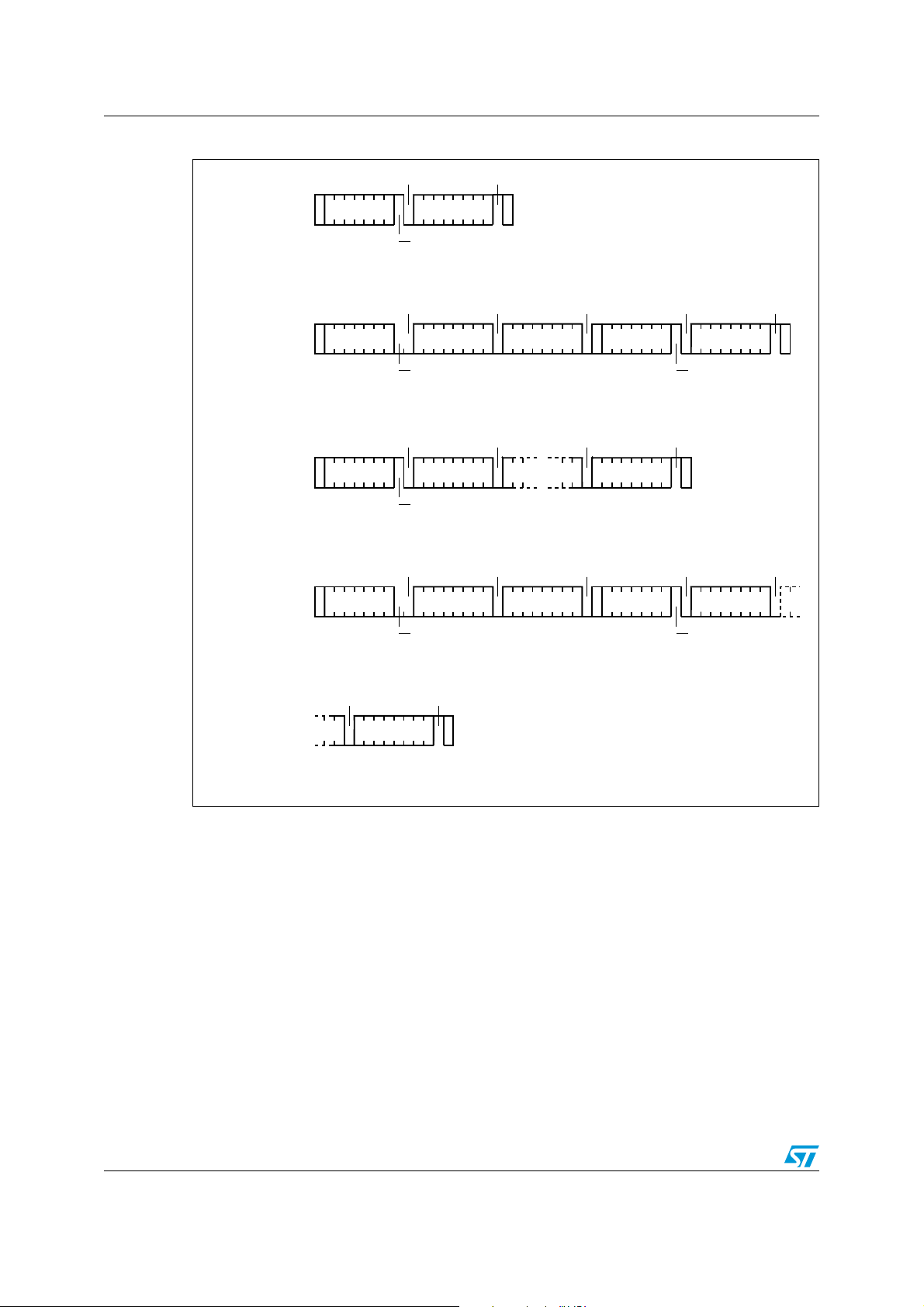
I2C device operation M24LR16E-R
Start
Dev select * Byte address Byte address
Start
Dev select Data out 1
AI01105d
Data out N
Stop
Start
Current
Address
Read
Dev select Data out
Random
Address
Read
Stop
Start
Dev select * Data out
Sequential
Current
Read
Stop
Data out N
Start
Dev select * Byte address Byte address
Sequential
Random
Read
Start
Dev select * Data out 1
Stop
ACK
R/W
NO ACK
ACK
R/W
ACK ACK ACK
R/W
ACK ACK ACK NO ACK
R/W
NO ACK
ACK ACK ACK
R/W
ACK ACK
R/W
ACK NO ACK
Figure 11. Read mode sequences
1. The seven most significant bits of the device select code of a random read (in the first and fourth bytes)
must be identical.
38/143 Doc ID 018932 Rev 8
Page 39

M24LR16E-R I2C device operation
5.11 Read operations
Read operations are performed independently of the state of the I2C_Write_Lock bit.
After the successful completion of a read operation, the device’s internal address counter is
incremented by one, to point to the next byte address.
5.12 Random Address Read
A dummy write is first performed to load the address into this address counter (as shown in
Figure 11) but without sending a Stop condition. Then, the bus master sends another Start
condition, and repeats the device select code, with the Read/Write
device acknowledges this, and outputs the contents of the addressed byte. The bus master
must not acknowledge the byte, and terminates the transfer with a Stop condition.
bit (RW) set to 1. The
5.13 Current Address Read
For the Current Address Read operation, following a Start condition, the bus master only
sends a device select code with the Read/Write
this, and outputs the byte addressed by the internal address counter. The counter is then
incremented. The bus master terminates the transfer with a Stop condition, as shown in
Figure 11, without acknowledging the byte.
bit (RW) set to 1. The device acknowledges
5.14 Sequential Read
This operation can be used after a Current Address Read or a Random Address Read. The
bus master does acknowledge the data byte output, and sends additional clock pulses so
that the device continues to output the next byte in sequence. To terminate the stream of
bytes, the bus master must not acknowledge the last byte, and must generate a Stop
condition, as shown in Figure 11.
The output data come from consecutive addresses, with the internal address counter
automatically incremented after each byte output. After the last memory address, the
address counter “rolls-over”, and the device continues to output data from memory
address 00h.
5.15 Acknowledge in Read mode
For all Read commands, the device waits, after each byte read, for an acknowledgment
during the ninth bit time. If the bus master does not drive Serial Data (SDA) low during this
time, the device terminates the data transfer and switches to its Standby mode.
Doc ID 018932 Rev 8 39/143
Page 40
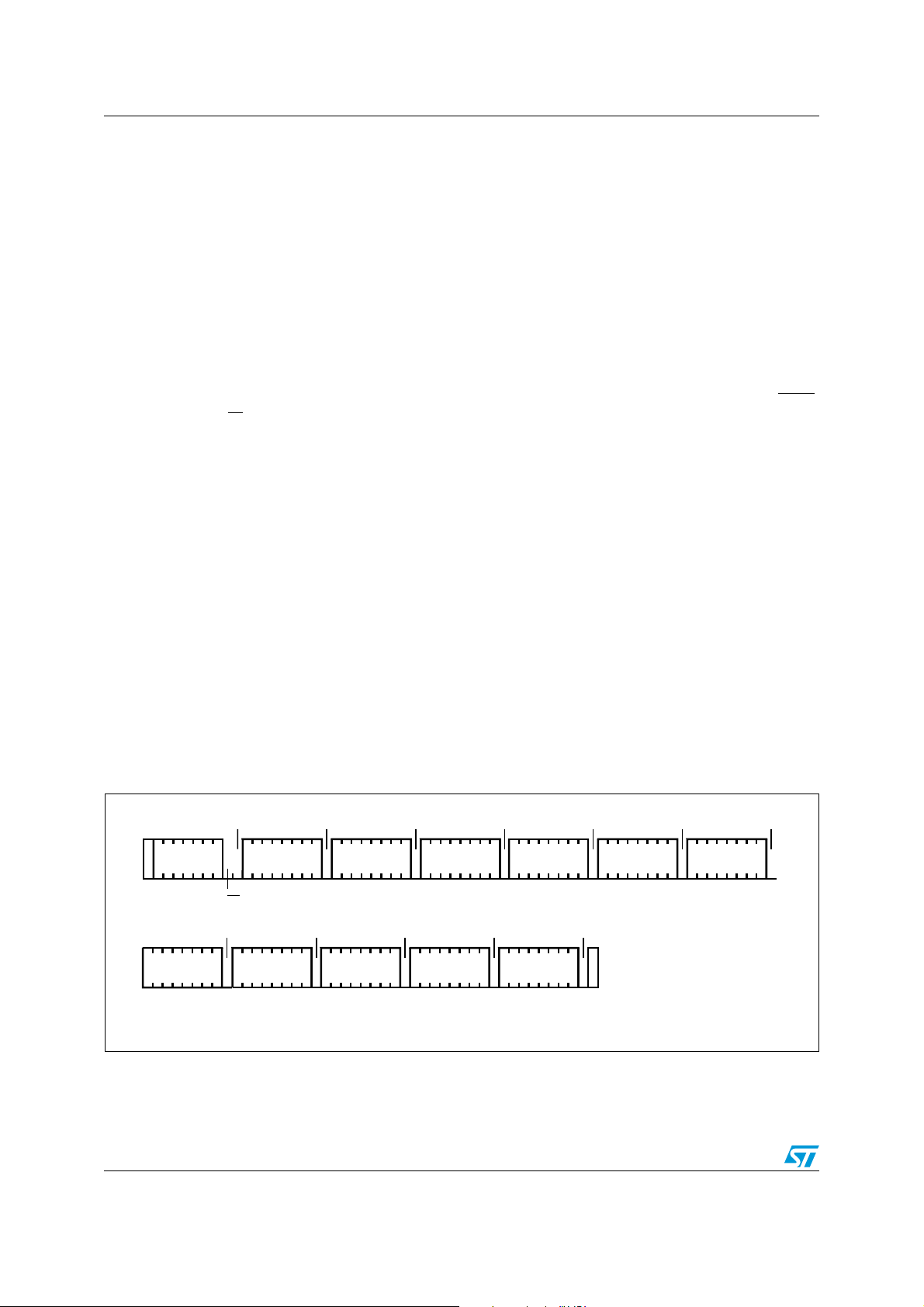
I2C device operation M24LR16E-R
ai15125c
Start
Device select
code
Password
address 09h
Password
address 00h
Password
[31:24]
Ack
R/W
Ack Ack Ack
Device select code = 1010 1 1 1
Password
[23:16]
Password
[15:8]
Password
[7:0]
Ack Ack Ack
Ack generated during
9
th
bit time slot.
Stop
Validation
code 09h
Ack
Password
[31:24]
Ack
Password
[23:16]
Password
[15:8]
Password
[7:0]
Ack Ack Ack
5.16 M24LR16E-R I2C password security
The M24LR16E-R controls I2C sector write access using the 32-bit-long I2C password and
the 64-bit I2C_Write_Lock bit area. The I
commands: I
2
C present password and I2C write password.
2
C password value is managed using two I2C
5.16.1 I2C present password command description
The I2C present password command is used in I2C mode to present the password to the
M24LR16E-R in order to modify the write access rights of all the memory sectors protected
by the I2C_Write_Lock bits, including the password itself. If the presented password is
correct, the access rights remain activated until the M24LR16E-R is powered off or until a
2
new I
C present password command is issued.
Following a Start condition, the bus master sends a device select code with the Read/Write
bit (RW
in Figure 12, and waits for two I
responds to each address byte with an acknowledge bit, and then waits for the four
password data bytes, the validation code, 09h, and a resend of the four password data
bytes. The most significant byte of the password is sent first, followed by the least significant
bytes.
It is necessary to send the 32-bit password twice to prevent any data corruption during the
sequence. If the two 32-bit passwords sent are not exactly the same, the M24LR16E-R does
not start the internal comparison.
When the bus master generates a Stop condition immediately after the Ack bit (during the
tenth bit time slot), an internal delay equivalent to the write cycle time is triggered. A Stop
condition at any other time does not trigger the internal delay. During that delay, the
M24LR16E-R compares the 32 received data bits with the 32 bits of the stored I
password. If the values match, the write access rights to all protected sectors are modified
after the internal delay. If the values do not match, the protected sectors remains protected.
) reset to 0 and the Chip Enable bit E2 at 1. The device acknowledges this, as shown
2
C password address bytes 09h and 00h. The device
2
C
Figure 12. I
40/143 Doc ID 018932 Rev 8
During the internal delay, the serial data (SDA) signal is disabled internally, and the device
does not respond to any requests.
2
C present password command
Page 41
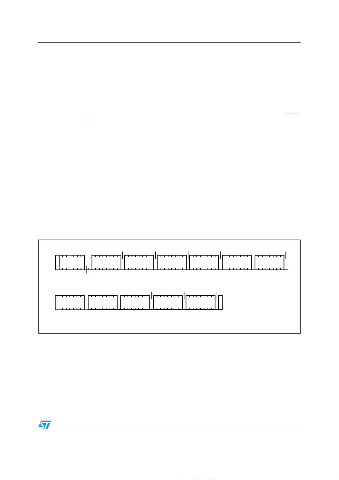
M24LR16E-R I2C device operation
ai15126b
Start
Device select
code
Password
address 09h
Password
address 00h
New password
[31:24]
Ack
R/W
Ack Ack Ack
Device select code = 1010 1 1 1
New password
[23:16]
New password
[15:8]
New password
[7:0]
Ack Ack Ack
Ack generated during
9
th
bit time slot.
Stop
Validation
code 07h
Ack
New password
[31:24]
Ack
New password
[23:16]
New password
[15:8]
New password
[7:0]
Ack Ack Ack
5.16.2 I2C write password command description
The I2C write password command is used to write a 32-bit block into the M24LR16E-R I2C
password system area. This command is used in I
2
C mode to update the I2C password
value. It cannot be used to update any of the RF passwords. After the write cycle, the new
2
I
C password value is automatically activated. The I2C password value can only be modified
after issuing a valid I
On delivery, the I
2
C present password command.
2
C default password value is set to 0000 0000h and is activated.
Following a Start condition, the bus master sends a device select code with the Read/Write
bit (RW
in Figure 13, and waits for the two I
) reset to 0 and the Chip Enable bit E2 at 1. The device acknowledges this, as shown
2
C password address bytes, 09h and 00h. The device
responds to each address byte with an acknowledge bit, and then waits for the four
password data bytes, the validation code, 07h, and a resend of the four password data
bytes. The most significant byte of the password is sent first, followed by the least significant
bytes.
It is necessary to send twice the 32-bit password to prevent any data corruption during the
write sequence. If the two 32-bit passwords sent are not exactly the same, the M24LR16E-R
does not modify the I
2
C password value.
When the bus master generates a Stop condition immediately after the Ack bit (during the
tenth bit time slot), the internal write cycle is triggered. A Stop condition at any other time
does not trigger the internal write cycle.
During the internal write cycle, the serial data (SDA) signal is disabled internally, and the
device does not respond to any requests.
Figure 13. I
2
C write password command
Doc ID 018932 Rev 8 41/143
Page 42

M24LR16E-R memory initial state M24LR16E-R
6 M24LR16E-R memory initial state
The device is delivered with all bits in the user memory array set to 1 (each byte contains
FFh).
The DSFID is programmed to FFh and the AFI is programmed to 00h.
Configuration byte set to F4h:
● Bit 7 to bit 4: all set to 1
● Bit 3: set to 0 (RF BUSY mode on RF WIP/BUSY pin)
● Bit 2: set to 1 (Energy harvesting not activated by default)
● Bit 1 and bit 0: set to 0
42/143 Doc ID 018932 Rev 8
Page 43

M24LR16E-R RF device operation
7 RF device operation
The M24LR16E-R is divided into 16 sectors of 32 blocks of 32 bits, as shown in Ta bl e 5 .
Each sector can be individually read- and/or write-protected using a specific lock or
password command.
Read and Write operations are possible if the addressed block is not protected. During a
Write, the 32 bits of the block are replaced by the new 32-bit value.
The M24LR16E-R also has a 64-bit block that is used to store the 64-bit unique identifier
(UID). The UID is compliant with the ISO 15963 description, and its value is used during the
anticollision sequence (Inventory). This block is not accessible by the user and its value is
written by ST on the production line.
The M24LR16E-R also includes an AFI register in which the application family identifier is
stored, and a DSFID register in which the data storage family identifier used in the
anticollision algorithm is stored.
The M24LR16E-R has three 32-bit blocks in which the password codes are stored and a 8bit Configuration byte in which the Energy harvesting mode and RF WIP/BUSY pin
configuration is stored.
7.1 RF communication and energy harvesting
Because current consumption can affect the AC signal delivered by the antenna, RF
communications with M24LR16E-R are not guaranteed during voltage delivery on the
energy harvesting analog output Vout.
RF communication can disturb and possibly stop Energy Harvesting mode.
Doc ID 018932 Rev 8 43/143
Page 44

RF device operation M24LR16E-R
7.2 Commands
The M24LR16E-R supports the following commands:
● Inventory, used to perform the anticollision sequence.
● Stay quiet, used to put the M24LR16E-R in quiet mode, where it does not respond to
any inventory command.
● Select, used to select the M24LR16E-R. After this command, the M24LR16E-R
processes all Read/Write commands with Select_flag set.
● Reset to ready, used to put the M24LR16E-R in the ready state.
● Read block, used to output the 32 bits of the selected block and its locking status.
● Write block, used to write the 32-bit value in the selected block, provided that it is not
locked.
● Read multiple blocks, used to read the selected blocks and send back their value.
● Write AFI, used to write the 8-bit value in the AFI register.
● Lock AFI, used to lock the AFI register.
● Write DSFID, used to write the 8-bit value in the DSFID register.
● Lock DSFID, used to lock the DSFID register.
● Get system info, used to provide the system information value
● Get multiple block security status, used to send the security status of the selected
block.
● Initiate, used to trigger the tag response to the Inventory initiated sequence.
● Inventory initiated, used to perform the anticollision sequence triggered by the Initiate
command.
● Write-sector password, used to write the 32 bits of the selected password.
● Lock-sector, used to write the sector security status bits of the selected sector.
● Present-sector password, enables the user to present a password to unprotect the
user blocks linked to this password.
● Fast initiate, used to trigger the tag response to the Inventory initiated sequence.
● Fast inventory initiated, used to perform the anticollision sequence triggered by the
Initiate command.
● Fast read single block, used to output the 32 bits of the selected block and its locking
status.
● Fast read multiple blocks, used to read the selected blocks and send back their value.
● ReadCfg, used to read the 8-bit Configuration byte and send back its value.
● WriteEHCfg, used to write the energy harvesting configuration bits into the
Configuration byte.
● WriteDOCfg, used to write the RF WIP/BUSY pin configuration bit into the
Configuration byte.
● SetRstEHEn, used to set or reset the EH_enable bit into the volatile Control register.
● CheckEHEn, used to send back the value of the volatile Control register.
44/143 Doc ID 018932 Rev 8
Page 45

M24LR16E-R RF device operation
7.3 Initial dialog for vicinity cards
The dialog between the vicinity coupling device or VCD (commonly the “RF reader”) and the
vicinity integrated circuit card or VICC (M24LR16E-R) takes place as follows:
● activation of the M24LR16E-R by the RF operating field of the VCD,
● transmission of a command by the VCD,
● transmission of a response by the M24LR16E-R.
These operations use the RF power transfer and communication signal interface described
below (see Power transfer, Frequency and Operating field). This technique is called RTF
(Reader talk first).
7.3.1 Power transfer
Power is transferred to the M24LR16E-R by radio frequency at 13.56 MHz via coupling
antennas in the M24LR16E-R and the VCD. The RF operating field of the VCD is
transformed on the M24LR16E-R antenna to an AC voltage which is rectified, filtered and
internally regulated.
During communications, the amplitude modulation (ASK) on this received signal is
demodulated by the ASK demodulator.
7.3.2 Frequency
The ISO 15693 standard defines the carrier frequency (fC) of the operating field as
13.56 MHz ±7 kHz.
7.3.3 Operating field
The M24LR16E-R operates continuously between the minimum and maximum values of the
electromagnetic field H defined in Table 124. The VCD has to generate a field within these
limits.
Doc ID 018932 Rev 8 45/143
Page 46
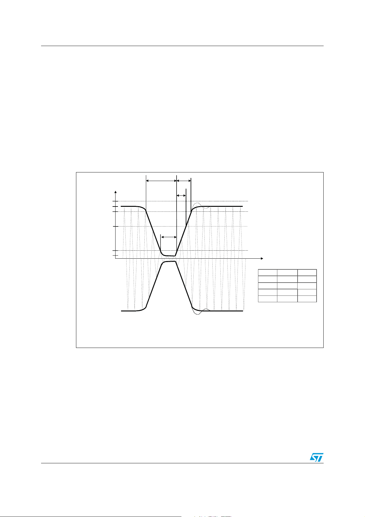
Communication signal from VCD to M24LR16E-R M24LR16E-R
105%
a
95%
5%
60%
Carrier
Amplitude
t
t
2
t
1
t
3
t
4
Min (µs)
t
1
6,0
t
2
2,1
t
3
0
Max (µs)
9,44
t
1
4,5
t
4
0 0,8
b
The clock recovery shall be operational after t
4
max.
ai15793
8 Communication signal from VCD to M24LR16E-R
Communications between the VCD and the M24LR16E-R takes place using the modulation
principle of ASK (Amplitude shift keying). Two modulation indexes are used, 10% and 100%.
The M24LR16E-R decodes both. The VCD determines which index is used.
The modulation index is defined as [a – b]/[a + b], where a is the peak signal amplitude, and
b the minimum signal amplitude of the carrier frequency.
Depending on the choice made by the VCD, a “pause” is created as described in Figure 14
and Figure 15.
The M24LR16E-R is operational for the 100% modulation index or for any degree of
modulation index between 10% and 30% (see Ta bl e 1 2 4).
Figure 14. 100% modulation waveform
46/143 Doc ID 018932 Rev 8
Page 47
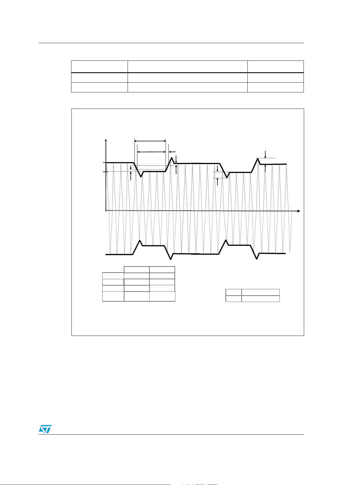
M24LR16E-R Communication signal from VCD to M24LR16E-R
Table 19. 10% modulation parameters
Symbol Parameter definition Value
hr 0.1 x (a – b) max
hf 0.1 x (a – b) max
Figure 15. 10% modulation waveform
Carrier
Carrier
Amplitude
Amplitude
a
a
b
b
t1
t1
t2
t2
y
y
t3
t3
y
y
hr
hr
hf
hf
t1
t1
t1
t2 3,0 µs
t2 3,0 µs
t2 3,0 µs
t3 0
t3 0
t3 0
Modulation
Modulation
Modulation
Index
Index
Index
Min
Min
Min
6,0 µs
6,0 µs
6,0 µs
10%
10%
10%
Max
Max
Max
9,44 µs
9,44 µs
9,44 µs
t1
t1
t1
4,5 µs
4,5 µs
4,5 µs
30%
30%
30%
y 0,05 (a-b)
y 0,05 (a-b)
y 0,05 (a-b)
hf, hr 0,1 (a-b) max
hf, hr 0,1 (a-b) max
hf, hr 0,1 (a-b) max
The VICC shall be operational for any value of modulation index between 10 % and 30 %.
ai15794
t
t
Doc ID 018932 Rev 8 47/143
Page 48
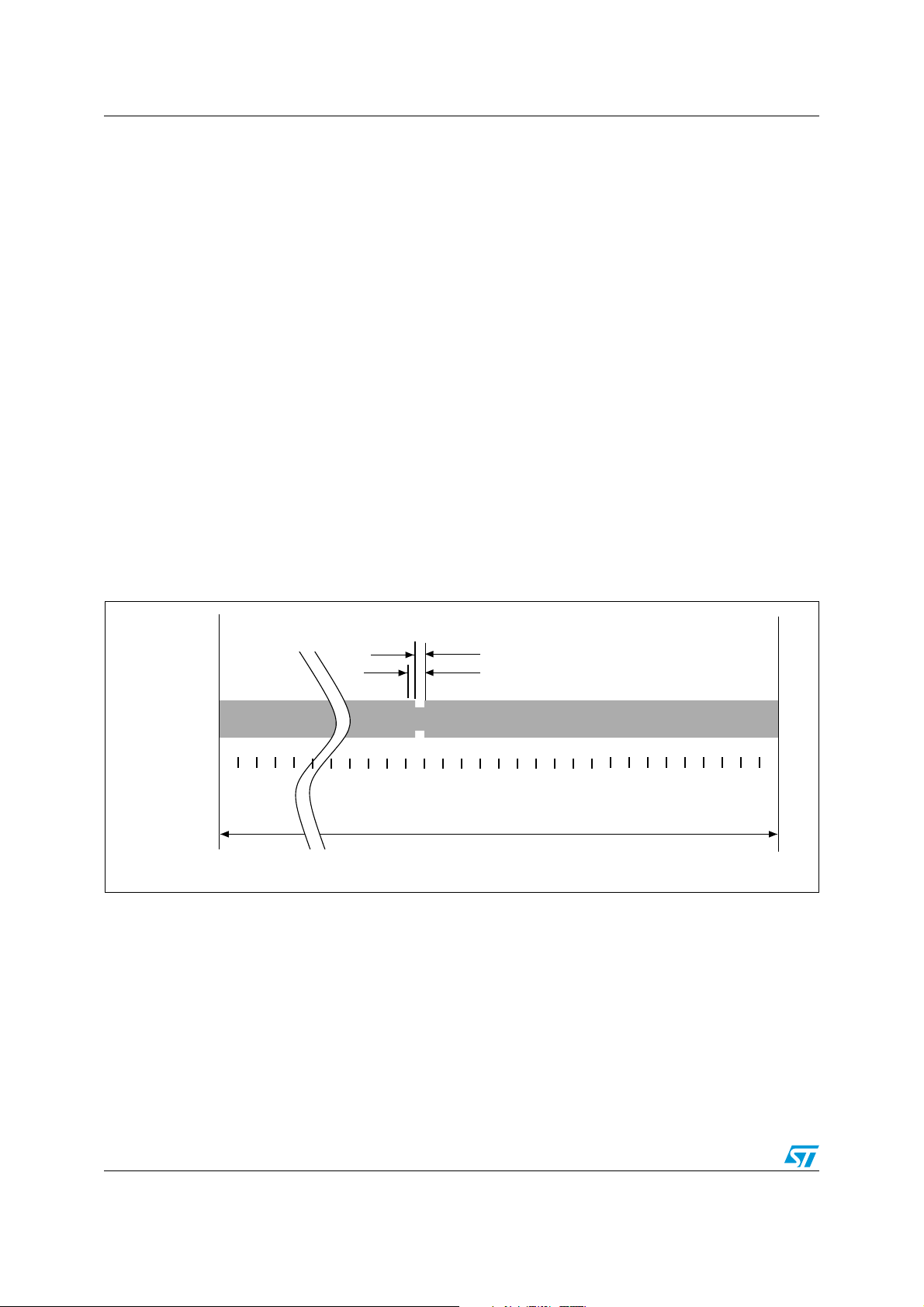
Data rate and data coding M24LR16E-R
AI06656
0 1 2 3 . . . . . . . . 2 . . . . . . . . . . . . . . . . . . . . . 2 2 2 2
. . . . . . . . . 2 . . . . . . . . . . . . . . . . . . . . . 5 5 5 5
. . . . . . . . . 5 . . . . . . . . . . . . . . . . . . . . . 2 3 4 5
4.833 ms
18.88 µs
9.44 µs
Pulse
Modulated
Carrier
9 Data rate and data coding
The data coding implemented in the M24LR16E-R uses pulse position modulation. Both
data coding modes that are described in the ISO15693 are supported by the M24LR16E-R.
The selection is made by the VCD and indicated to the M24LR16E-R within the start of
frame (SOF).
9.1 Data coding mode: 1 out of 256
The value of one single byte is represented by the position of one pause. The position of the
pause on 1 of 256 successive time periods of 18.88 µs (256/f
byte. In this case, the transmission of one byte takes 4.833 ms and the resulting data rate is
1.65 Kbits/s (f
/8192).
C
Figure 16 illustrates this pulse position modulation technique. In this figure, data E1h (225
decimal) is sent by the VCD to the M24LR16E-R.
The pause occurs during the second half of the position of the time period that determines
the value, as shown in Figure 17.
A pause during the first period transmits the data value 00h. A pause during the last period
transmits the data value FFh (255 decimal).
) determines the value of the
C
Figure 16. 1 out of 256 coding mode
48/143 Doc ID 018932 Rev 8
Page 49
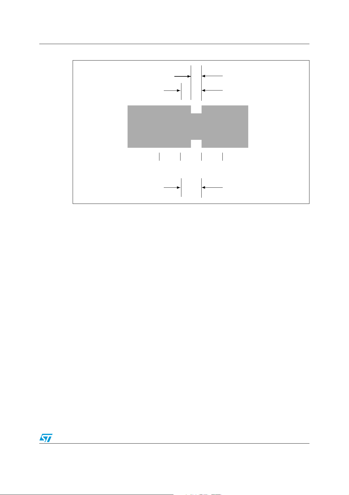
M24LR16E-R Data rate and data coding
AI06657
2
2
5
18.88 µs
9.44 µs
Pulse
Modulated
Carrier
2
2
6
2
2
4
. . . . . . .. . . . . . .
Time Period
one of 256
Figure 17. Detail of a time period
9.2 Data coding mode: 1 out of 4
The value of two bits is represented by the position of one pause. The position of the pause
on 1 of 4 successive time periods of 18.88 µs (256/f
Four successive pairs of bits form a byte, where the least significant pair of bits is
transmitted first.
In this case, the transmission of one byte takes 302.08 µs and the resulting data rate is
26.48 Kbits/s (f
coding. Figure 19 shows the transmission of E1h (225d - 1110 0001b) by the VCD.
/512). Figure 18 illustrates the 1 out of 4 pulse position technique and
C
) determines the value of the two bits.
C
Doc ID 018932 Rev 8 49/143
Page 50
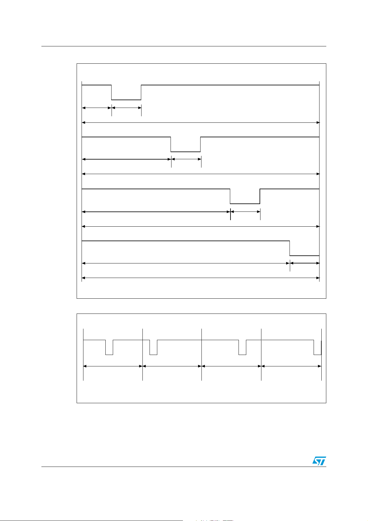
Data rate and data coding M24LR16E-R
AI06658
9.44 µs 9.44 µs
75.52 µs
28.32 µs 9.44 µs
75.52 µs
47.20µs 9.44 µs
75.52 µs
66.08 µs 9.44 µs
75.52 µs
Pulse position for "00"
Pulse position for "11"
Pulse position for "10" (0=LSB)
Pulse position for "01" (1=LSB)
AI06659
75.52µs75.52µs 75.52µs 75.52µs
00
10
01 11
Figure 18. 1 out of 4 coding mode
50/143 Doc ID 018932 Rev 8
Figure 19. 1 out of 4 coding example
Page 51
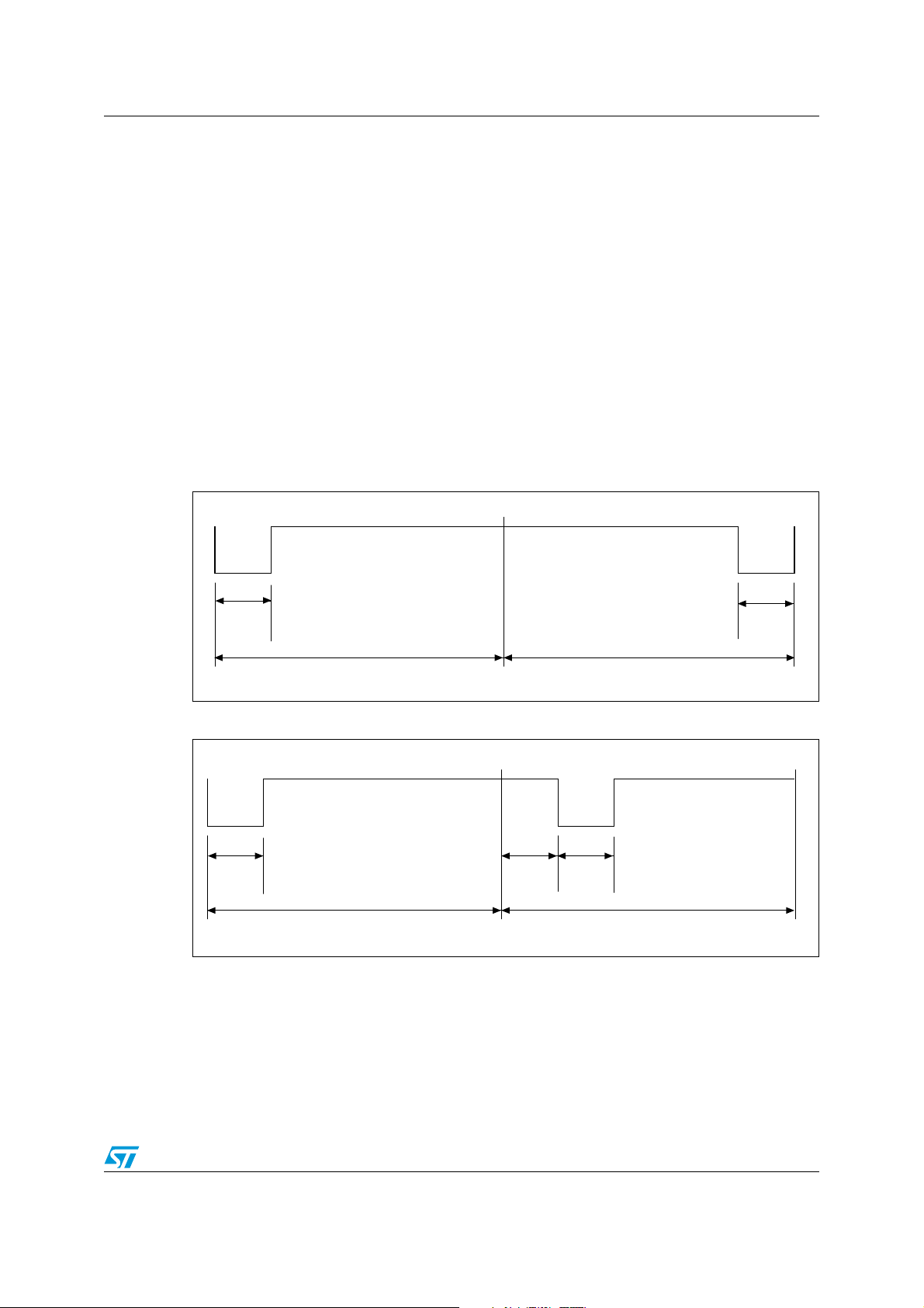
M24LR16E-R Data rate and data coding
AI06661
37.76µs
9.44µs
9.44µs
37.76µs
AI06660
37.76µs
9.44µs
9.44µs
37.76µs
9.44µs
9.3 VCD to M24LR16E-R frames
Frames are delimited by a start of frame (SOF) and an end of frame (EOF). They are
implemented using code violation. Unused options are reserved for future use.
The M24LR16E-R is ready to receive a new command frame from the VCD 311.5 µs (t
after sending a response frame to the VCD.
The M24LR16E-R takes a power-up time of 0.1 ms after being activated by the powering
field. After this delay, the M24LR16E-R is ready to receive a command frame from the VCD.
9.4 Start of frame (SOF)
The SOF defines the data coding mode the VCD is to use for the following command frame.
The SOF sequence described in Figure 20 selects the 1 out of 256 data coding mode. The
SOF sequence described in Figure 21 selects the 1 out of 4 data coding mode. The EOF
sequence for either coding mode is described in Figure 22.
Figure 20. SOF to select 1 out of 256 data coding mode
)
2
Figure 21. SOF to select 1 out of 4 data coding mode
Doc ID 018932 Rev 8 51/143
Page 52
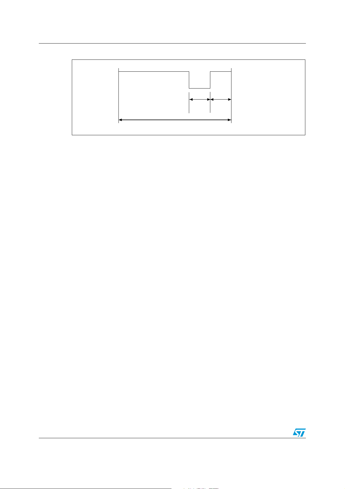
Data rate and data coding M24LR16E-R
AI06662
9.44µs
37.76µs
9.44µs
Figure 22. EOF for either data coding mode
52/143 Doc ID 018932 Rev 8
Page 53
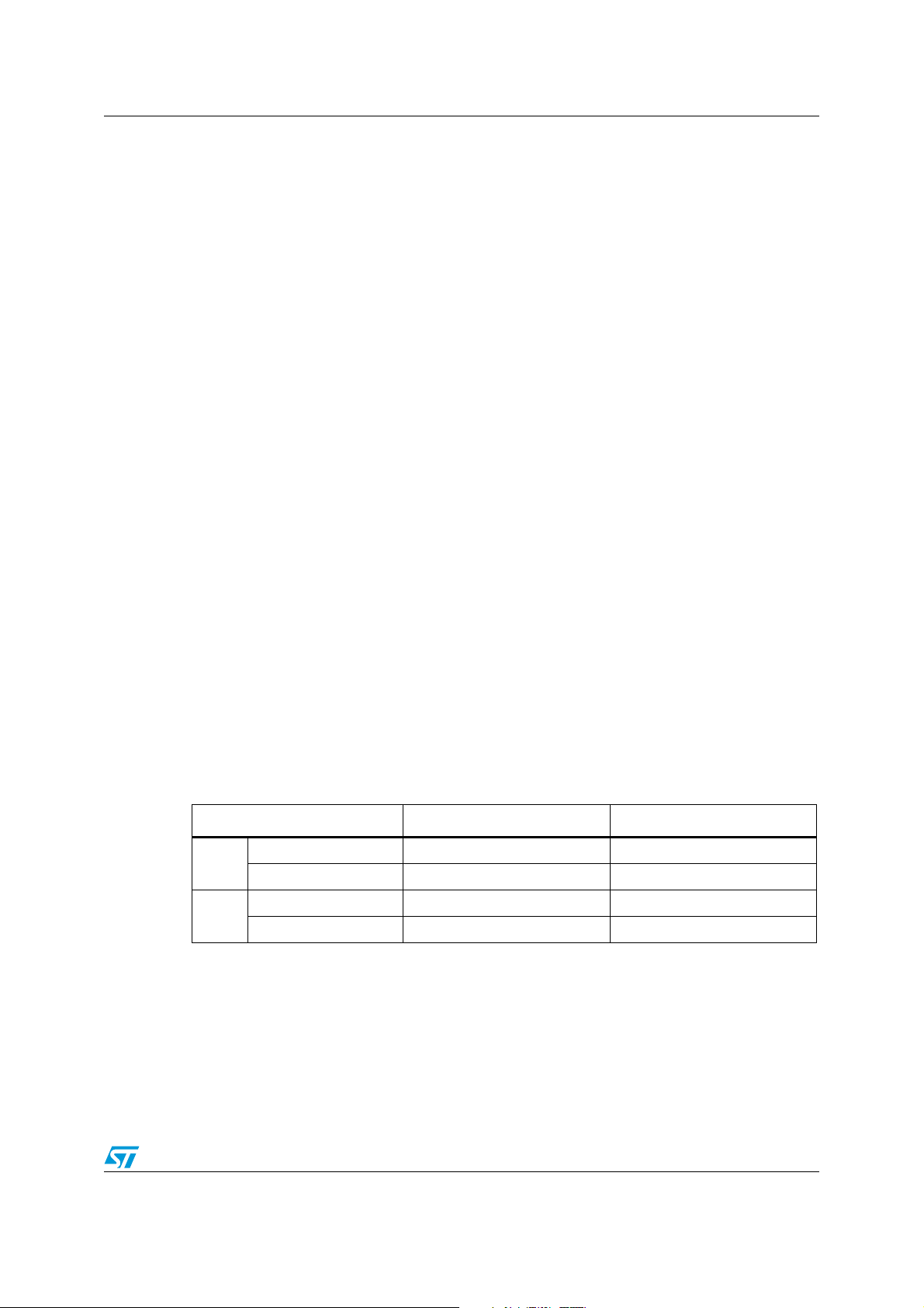
M24LR16E-R Communication signal from M24LR16E-R to VCD
10 Communication signal from M24LR16E-R to VCD
The M24LR16E-R has several modes defined for some parameters, owing to which it can
operate in various noise environments and meet various application requirements.
10.1 Load modulation
The M24LR16E-R is capable of communication to the VCD via an inductive coupling area
whereby the carrier is loaded to generate a subcarrier with frequency f
generated by switching a load in the M24LR16E-R.
The load-modulated amplitude received on the VCD antenna must be of at least 10 mV
when measured as described in the test methods defined in International Standard
ISO10373-7.
10.2 Subcarrier
The M24LR16E-R supports the one-subcarrier and two-subcarrier response formats. These
formats are selected by the VCD using the first bit in the protocol header. When one
subcarrier is used, the frequency f
When two subcarriers are used, the frequency f
is 484.28 kHz (f
continuous phase relationship between f
of the subcarrier load modulation is 423.75 kHz (fC/32).
S1
/28). When using the two-subcarrier mode, the M24LR16E-R generates a
C
and fS2.
S1
is 423.75 kHz (fC/32), and frequency fS2
S1
. The subcarrier is
S
10.3 Data rates
The M24LR16E-R can respond using the low or the high data rate format. The selection of
the data rate is made by the VCD using the second bit in the protocol header. For fast
commands, the selected data rate is multiplied by two. Ta b le 2 0 shows the different data
rates produced by the M24LR16E-R using the different response format combinations.
Table 20. Response data rates
Data rate One subcarrier Two subcarriers
Standard commands 6.62 Kbit/s (f
Low
Fast commands 13.24 Kbit/s (f
High
Standard commands 26.48 Kbit/s (f
Fast commands 52.97 Kbit/s (f
/2048) 6.67 Kbit/s (fc/2032)
c
/1024) not applicable
c
/512) 26.69 Kbit/s (fc/508)
c
/256) not applicable
c
Doc ID 018932 Rev 8 53/143
Page 54
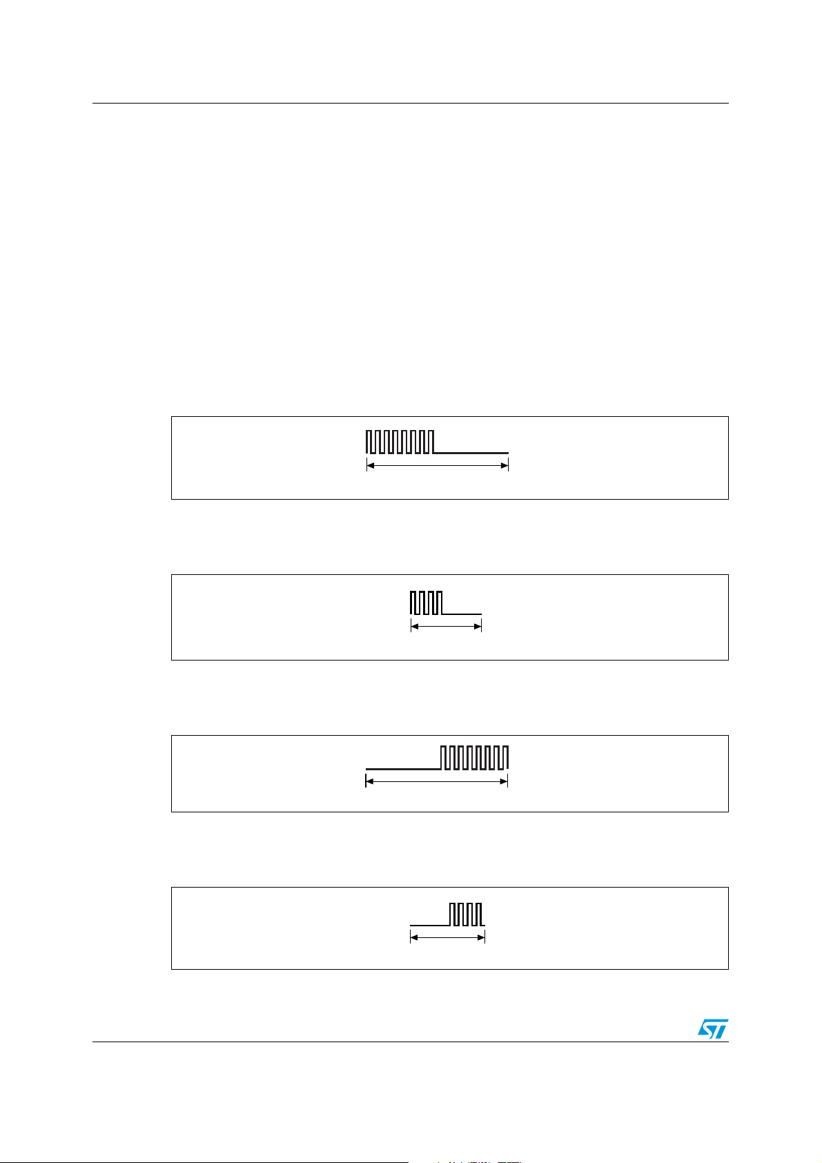
Bit representation and coding M24LR16E-R
37.76µs
ai12076
18.88µs
ai12066
37.76µs
ai12077
18.88µs
ai12067
11 Bit representation and coding
Data bits are encoded using Manchester coding, according to the following schemes. For
the low data rate, same subcarrier frequency or frequencies is/are used. In this case, the
number of pulses is multiplied by 4 and all times increase by this factor. For the Fast
commands using one subcarrier, all pulse numbers and times are divided by 2.
11.1 Bit coding using one subcarrier
11.1.1 High data rate
A logic 0 starts with eight pulses at 423.75 kHz (fC/32) followed by an unmodulated time of
18.88 µs, as shown in Figure 23.
Figure 23. Logic 0, high data rate
For the fast commands, a logic 0 starts with four pulses at 423.75 kHz (f
/32) followed by an
C
unmodulated time of 9.44 µs, as shown in Figure 24.
Figure 24. Logic 0, high data rate, fast commands
A logic 1 starts with an unmodulated time of 18.88 µs followed by eight pulses at 423.75 kHz
(f
/32), as shown in Figure 25.
C
Figure 25. Logic 1, high data rate
For the Fast commands, a logic 1 starts with an unmodulated time of 9.44 µs followed by
four pulses of 423.75 kHz (f
/32), as shown in Figure 26.
C
Figure 26. Logic 1, high data rate, fast commands
54/143 Doc ID 018932 Rev 8
Page 55
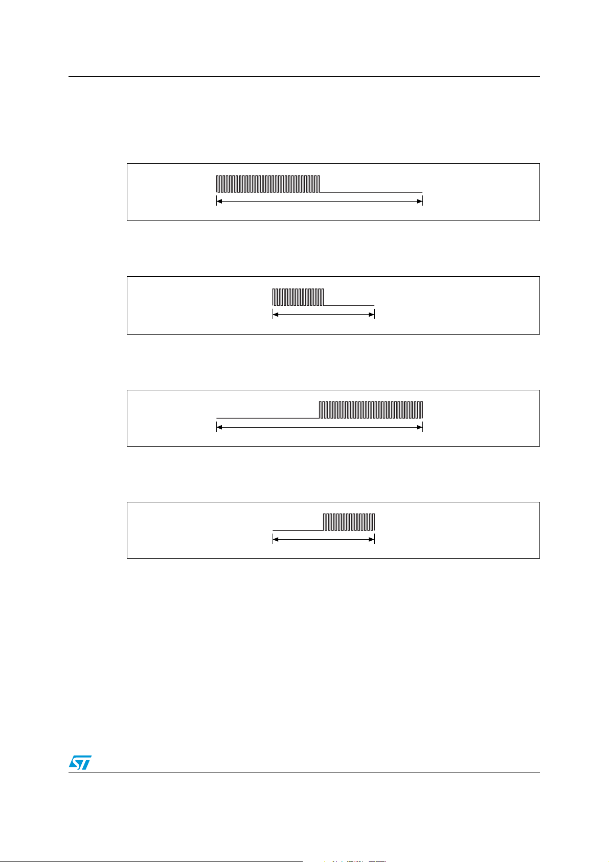
M24LR16E-R Bit representation and coding
151.04µs
ai12068
75.52µs
ai12069
151.04µs
ai12070
75.52µs
ai12071
11.1.2 Low data rate
A logic 0 starts with 32 pulses at 423.75 kHz (fC/32) followed by an unmodulated time of
75.52 µs, as shown in Figure 27.
Figure 27. Logic 0, low data rate
For the Fast commands, a logic 0 starts with 16 pulses at 423.75 kHz (f
/32) followed by an
C
unmodulated time of 37.76 µs, as shown in Figure 28.
Figure 28. Logic 0, low data rate, fast commands
A logic 1 starts with an unmodulated time of 75.52 µs followed by 32 pulses at 423.75 kHz
(f
/32), as shown in Figure 29.
C
Figure 29. Logic 1, low data rate
For the Fast commands, a logic 1 starts with an unmodulated time of 37.76 µs followed by
16 pulses at 423.75 kHz (f
/32), as shown in Figure 30.
C
Figure 30. Logic 1, low data rate, fast commands
Doc ID 018932 Rev 8 55/143
Page 56
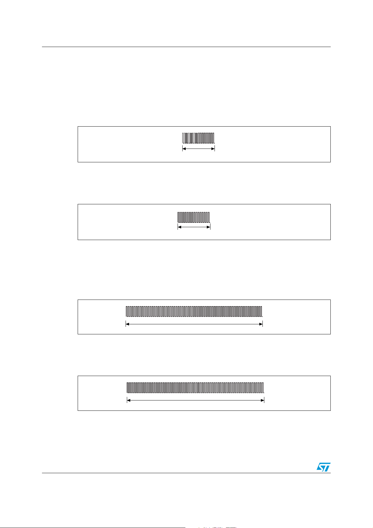
Bit representation and coding M24LR16E-R
37.46µs
ai12074
37.46µs
ai12073
149.84µs
ai12072
149.84µs
ai12075
11.2 Bit coding using two subcarriers
11.2.1 High data rate
A logic 0 starts with eight pulses at 423.75 kHz (fC/32) followed by nine pulses at
484.28 kHz (f
for the Fast commands.
Figure 31. Logic 0, high data rate
/28), as shown in Figure 31. Bit coding using two subcarriers is not supported
C
A logic 1 starts with nine pulses at 484.28 kHz (f
423.75 kHz (f
/32), as shown in Figure 32. Bit coding using two subcarriers is not supported
C
for the Fast commands.
Figure 32. Logic 1, high data rate
11.2.2 Low data rate
A logic 0 starts with 32 pulses at 423.75 kHz (fC/32) followed by 36 pulses at 484.28 kHz
(f
/28), as shown in Figure 33. Bit coding using two subcarriers is not supported for the Fast
C
commands.
Figure 33. Logic 0, low data rate
A logic 1 starts with 36 pulses at 484.28 kHz (f
(f
/32) as shown in Figure 34. Bit coding using two subcarriers is not supported for the Fast
C
commands.
/28) followed by eight pulses at
C
/28) followed by 32 pulses at 423.75 kHz
C
Figure 34. Logic 1, low data rate
56/143 Doc ID 018932 Rev 8
Page 57
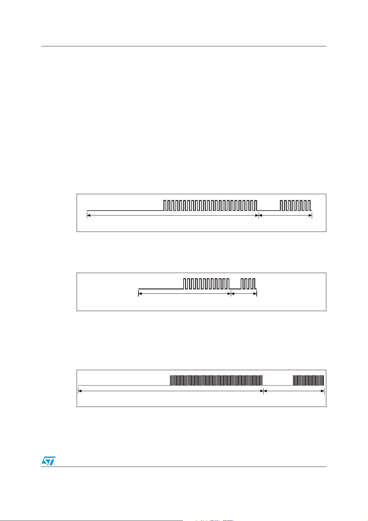
M24LR16E-R M24LR16E-R to VCD frames
113.28µs
ai12078
37.76µs
56.64µs
ai12079
18.88µs
453.12µs
ai12080
151.04µs
12 M24LR16E-R to VCD frames
Frames are delimited by an SOF and an EOF. They are implemented using code violation.
Unused options are reserved for future use. For the low data rate, the same subcarrier
frequency or frequencies is/are used. In this case, the number of pulses is multiplied by 4.
For the Fast commands using one subcarrier, all pulse numbers and times are divided by 2.
12.1 SOF when using one subcarrier
12.1.1 High data rate
The SOF includes an unmodulated time of 56.64 µs, followed by 24 pulses at 423.75 kHz
(f
/32), and a logic 1 that consists of an unmodulated time of 18.88 µs followed by eight
C
pulses at 423.75 kHz, as shown in Figure 35.
Figure 35. Start of frame, high data rate, one subcarrier
For the Fast commands, the SOF comprises an unmodulated time of 28.32 µs, followed by
12 pulses at 423.75 kHz (f
9.44 µs followed by four pulses at 423.75 kHz, as shown in Figure 36.
Figure 36. Start of frame, high data rate, one subcarrier, fast commands
12.1.2 Low data rate
The SOF comprises an unmodulated time of 226.56 µs, followed by 96 pulses at 423.75 kHz
(f
/32), and a logic 1 that consists of an unmodulated time of 75.52 µs followed by 32 pulses
C
at 423.75 kHz, as shown in Figure 37.
Figure 37. Start of frame, low data rate, one subcarrier
/32), and a logic 1 that consists of an unmodulated time of
C
Doc ID 018932 Rev 8 57/143
Page 58
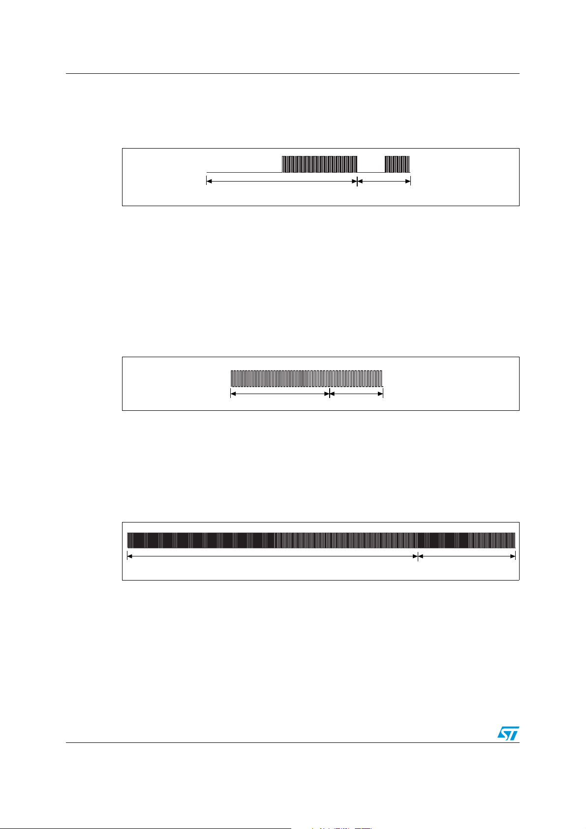
M24LR16E-R to VCD frames M24LR16E-R
226.56µs
ai12081
75.52µs
112.39µs
ai12082
37.46µs
449.56µs
ai12083
149.84µs
For the Fast commands, the SOF comprises an unmodulated time of 113.28 µs, followed by
48 pulses at 423.75 kHz (f
/32), and a logic 1 that includes an unmodulated time of 37.76 µs
C
followed by 16 pulses at 423.75 kHz, as shown in Figure 38.
Figure 38. Start of frame, low data rate, one subcarrier, fast commands
12.2 SOF when using two subcarriers
12.2.1 High data rate
The SOF comprises 27 pulses at 484.28 kHz (fC/28), followed by 24 pulses at 423.75 kHz
(f
/32), and a logic 1 that includes nine pulses at 484.28 kHz followed by eight pulses at
C
423.75 kHz, as shown in Figure 39.
Bit coding using two subcarriers is not supported for the Fast commands.
Figure 39. Start of frame, high data rate, two subcarriers
12.2.2 Low data rate
The SOF comprises 108 pulses at 484.28 kHz (fC/28), followed by 96 pulses at 423.75 kHz
(f
/32), and a logic 1 that includes 36 pulses at 484.28 kHz followed by 32 pulses at
C
423.75 kHz, as shown in Figure 40.
Bit coding using two subcarriers is not supported for the Fast commands.
Figure 40. Start of frame, low data rate, two subcarriers
58/143 Doc ID 018932 Rev 8
Page 59
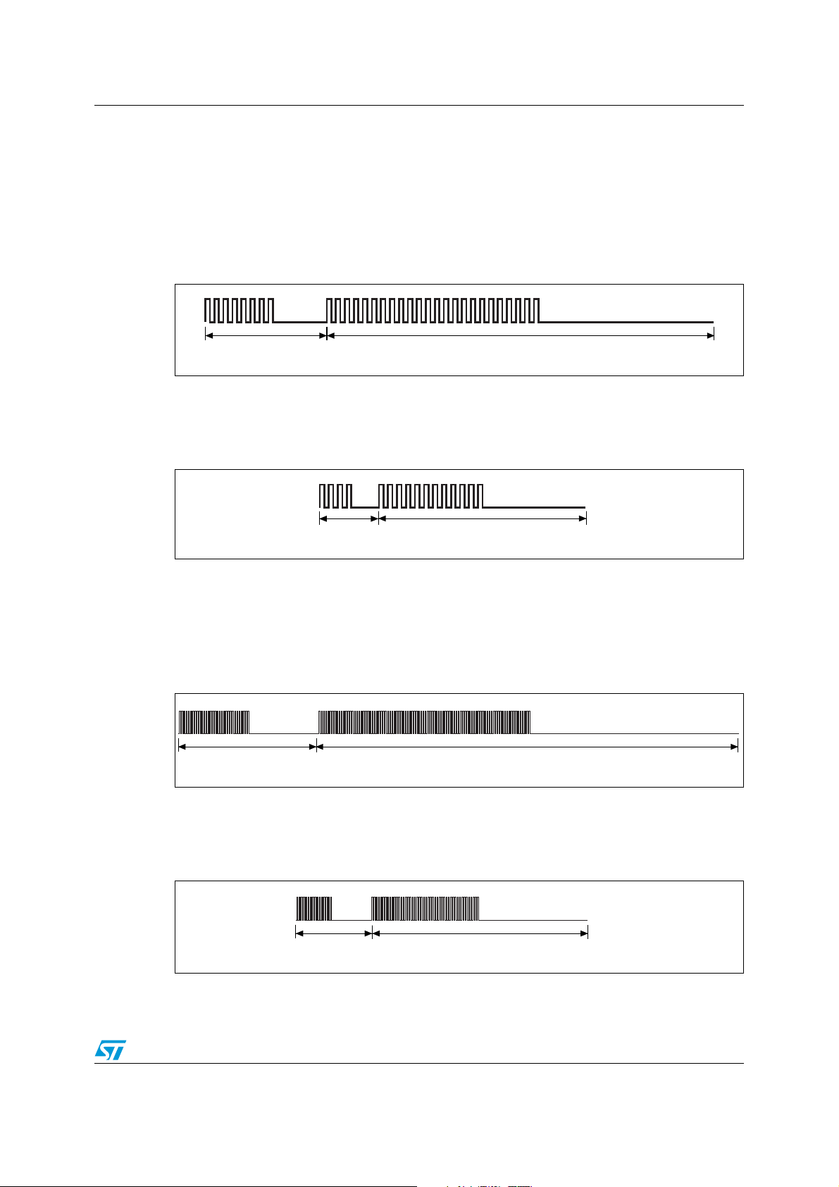
M24LR16E-R M24LR16E-R to VCD frames
113.28µs
ai12084
37.76µs
56.64µs
ai12085
18.88µs
453.12µs
ai12086
151.04µs
226.56µs
ai12087
75.52µs
12.3 EOF when using one subcarrier
12.3.1 High data rate
The EOF comprises a logic 0 that includes eight pulses at 423.75 kHz and an unmodulated
time of 18.88 µs, followed by 24 pulses at 423.75 kHz (f
of 56.64 µs, as shown in Figure 41.
Figure 41. End of frame, high data rate, one subcarrier
For the Fast commands, the EOF comprises a logic 0 that includes four pulses at
423.75 kHz and an unmodulated time of 9.44 µs, followed by 12 pulses at 423.75 kHz
(f
/32) and an unmodulated time of 37.76 µs, as shown in Figure 42.
C
Figure 42. End of frame, high data rate, one subcarrier, fast commands
/32), and by an unmodulated time
C
12.3.2 Low data rate
The EOF comprises a logic 0 that includes 32 pulses at 423.75 kHz and an unmodulated
time of 75.52 µs, followed by 96 pulses at 423.75 kHz (f
226.56 µs, as shown in Figure 43.
Figure 43. End of frame, low data rate, one subcarrier
For the Fast commands, the EOF comprises a logic 0 that includes 16 pulses at 423.75 kHz
and an unmodulated time of 37.76 µs, followed by 48 pulses at 423.75 kHz (f
unmodulated time of 113.28 µs, as shown in Figure 44.
Figure 44. End of frame, low data rate, one subcarrier, Fast commands
/32) and an unmodulated time of
C
/32) and an
C
Doc ID 018932 Rev 8 59/143
Page 60
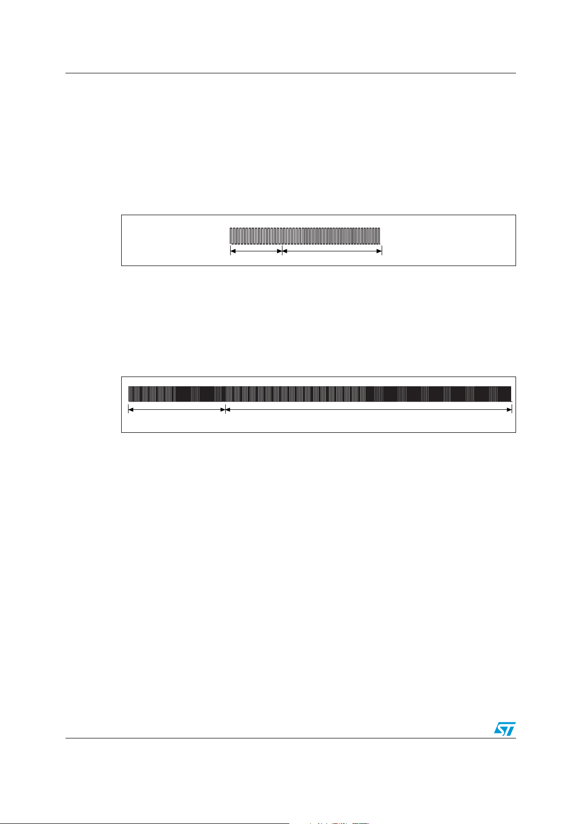
M24LR16E-R to VCD frames M24LR16E-R
112.39µs
ai12088
37.46µs
449.56µs
ai12089
149.84µs
12.4 EOF when using two subcarriers
12.4.1 High data rate
The EOF comprises a logic 0 that includes eight pulses at 423.75 kHz and nine pulses at
484.28 kHz, followed by 24 pulses at 423.75 kHz (f
(f
/28), as shown in Figure 45.
C
Bit coding using two subcarriers is not supported for the Fast commands.
Figure 45. End of frame, high data rate, two subcarriers
12.4.2 Low data rate
The EOF comprises a logic 0 that includes 32 pulses at 423.75 kHz and 36 pulses at
484.28 kHz, followed by 96 pulses at 423.75 kHz (f
(f
/28), as shown in Figure 46.
C
Bit coding using two subcarriers is not supported for the Fast commands.
/32) and 27 pulses at 484.28 kHz
C
/32) and 108 pulses at 484.28 kHz
C
Figure 46. End of frame, low data rate, two subcarriers
60/143 Doc ID 018932 Rev 8
Page 61
M24LR16E-R Unique identifier (UID)
13 Unique identifier (UID)
The M24LR16E-R is uniquely identified by a 64-bit unique identifier (UID). This UID
complies with ISO/IEC 15963 and ISO/IEC 7816-6. The UID is a read-only code and
comprises:
● eight MSBs with a value of E0h,
● the IC manufacturer code “ST 02h” on 8 bits (ISO/IEC 7816-6/AM1),
● a unique serial number on 48 bits.
Table 21. UID format
MSB LSB
63 56 55 48 47 0
0xE0 0x02 Unique serial number
With the UID, each M24LR16E-R can be addressed uniquely and individually during the
anticollision loop and for one-to-one exchanges between a VCD and an M24LR16E-R.
Doc ID 018932 Rev 8 61/143
Page 62
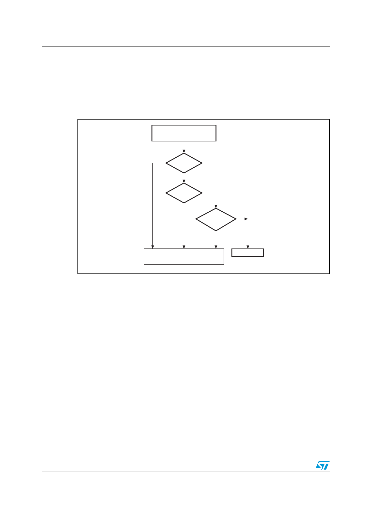
Application family identifier (AFI) M24LR16E-R
14 Application family identifier (AFI)
The AFI (application family identifier) represents the type of application targeted by the VCD
and is used to identify, among all the M24LR16E-Rs present, only the M24LR16E-Rs that
meet the required application criteria.
Figure 47. M24LR16E-R decision tree for AFI
Inventory request
received
No
Answer given by the M24RF64
AFI flag
set ?
Yes
AFI value
= 0 ?
Yes
to the Inventory request
No
AFI value
= Internal
value ?
No
Yes
No answer
AI15130
The AFI is programmed by the M24LR16E-R issuer (or purchaser) in the AFI register. Once
programmed and locked, it can no longer be modified.
The most significant nibble of the AFI is used to code one specific or all application families.
The least significant nibble of the AFI is used to code one specific or all application
subfamilies. Subfamily codes different from 0 are proprietary.
(See ISO 15693-3 documentation.)
62/143 Doc ID 018932 Rev 8
Page 63
M24LR16E-R Data storage format identifier (DSFID)
15 Data storage format identifier (DSFID)
The data storage format identifier indicates how the data is structured in the M24LR16E-R
memory. The logical organization of data can be known instantly using the DSFID. It can be
programmed and locked using the Write DSFID and Lock DSFID commands.
15.1 CRC
The CRC used in the M24LR16E-R is calculated as per the definition in ISO/IEC 13239. The
initial register contents are all ones: “FFFF”.
The two-byte CRC is appended to each request and response, within each frame, before
the EOF. The CRC is calculated on all the bytes after the SOF up to the CRC field.
Upon reception of a request from the VCD, the M24LR16E-R verifies that the CRC value is
valid. If it is invalid, the M24LR16E-R discards the frame and does not answer to the VCD.
Upon reception of a response from the M24LR16E-R, it is recommended that the VCD
verifies whether the CRC value is valid. If it is invalid, actions to be performed are left to the
discretion of the VCD designer.
The CRC is transmitted least significant byte first. Each byte is transmitted least significant
bit first.
Table 22. CRC transmission rules
LSBit MSBit
LSByte
LSBit MSBit
CRC 16 (8 bits) CRC 16 (8 bits)
MSByte
Doc ID 018932 Rev 8 63/143
Page 64

M24LR16E-R protocol description M24LR16E-R
16 M24LR16E-R protocol description
The transmission protocol (or simply “the protocol”) defines the mechanism used to
exchange instructions and data between the VCD and the M24LR16E-R in both directions.
It is based on the concept of “VCD talks first”.
This means that an M24LR16E-R does not start transmitting unless it has received and
properly decoded an instruction sent by the VCD. The protocol is based on an exchange of:
● a request from the VCD to the M24LR16E-R,
● a response from the M24LR16E-R to the VCD.
Each request and each response are contained in a frame. The frame delimiters (SOF,
EOF) are described in Section 12.
Each request consists of:
● a request SOF (see Figure 20 and Figure 21),
● flags,
● a command code,
● parameters depending on the command,
● application data,
● a 2-byte CRC,
● a request EOF (see Figure 22).
Each response consists of:
● an answer SOF (see Figure 35 to Figure 40),
● flags,
● parameters depending on the command,
● application data,
● a 2-byte CRC,
● an answer EOF (see Figure 41 to Figure 46).
The protocol is bit-oriented. The number of bits transmitted in a frame is a multiple of eight
(8), that is an integer number of bytes.
A single-byte field is transmitted least significant bit (LSBit) first. A multiple-byte field is
transmitted least significant byte (LSByte) first and each byte is transmitted least significant
bit (LSBit) first.
The setting of the flags indicates the presence of the optional fields. When the flag is set (to
one), the field is present. When the flag is reset (to zero), the field is absent.
Table 23. VCD request frame format
Request SOF Request_flags
Table 24. M24LR16E-R Response frame format
Response
SOF
Response_flags Parameters Data 2-byte CRC
Command
code
Parameters Data 2-byte CRC
Request
EOF
Response
EOF
64/143 Doc ID 018932 Rev 8
Page 65

M24LR16E-R M24LR16E-R protocol description
Figure 48. M24LR16E-R protocol timing
Request
VCD
frame
(Ta bl e 2 3 )
M24LR16
E-R
Timing <-t
Request
frame
(Ta bl e 2 3 )
Response
frame
(Ta bl e 2 4 )
-> <-t2-> <-t1-> <-t2->
1
Response
frame
(Ta bl e 2 4 )
Doc ID 018932 Rev 8 65/143
Page 66

M24LR16E-R states M24LR16E-R
17 M24LR16E-R states
An M24LR16E-R can be in one of four states:
● Power-off
● Ready
● Quiet
● Selected
Transitions between these states are specified in Figure 49 and Ta bl e 2 5 .
17.1 Power-off state
The M24LR16E-R is in the Power-off state when it does not receive enough energy from the
VCD.
17.2 Ready state
The M24LR16E-R is in the Ready state when it receives enough energy from the VCD.
When in the Ready state, the M24LR16E-R answers any request where the Select_flag is
not set.
17.3 Quiet state
When in the Quiet state, the M24LR16E-R answers any request except for Inventory
requests with the Address_flag set.
17.4 Selected state
In the Selected state, the M24LR16E-R answers any request in all modes (see Section 18):
● Request in Select mode with the Select_flag set
● Request in Addressed mode if the UID matches
● Request in Non-Addressed mode as it is the mode for general requests
66/143 Doc ID 018932 Rev 8
Page 67
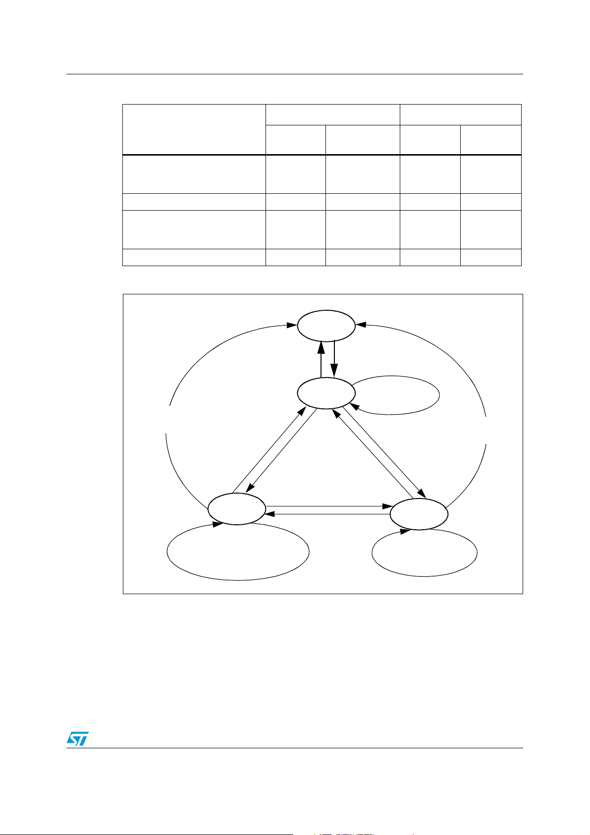
M24LR16E-R M24LR16E-R states
AI06681b
Power-off
In field
Out of field
Ready
Quiet
Selected
Any other Command
where Select_Flag
is not set
Stay quiet(UID)
Select (UID)
Any other command
Any other command where the
Address_Flag is set AND
where Inventory_Flag is not set
Stay quiet(UID)
Select
(UID)
Reset to ready where
Select_Flag is set or
Select(different
UID)
Reset to ready
Out of RF field
after t
RF_OFF
Out of RF field
after t
RF_OFF
after t
RF_OFF
Table 25. M24LR16E-R response depending on Request_flags
Address_flag Select_flag
Flags
1
Addressed0Non addressed
1
Selected0Non selected
M24LR16E-R in Ready or
Selected state (Devices in Quiet
XX
state do not answer)
M24LR16E-R in Selected state X X
M24LR16E-R in Ready, Quiet or
Selected state (the device which
XX
matches the UID)
Error (03h) X X
Figure 49. M24LR16E-R state transition diagram
1. The M24LR16E-R returns to the Power Off state if the tag is out of the RF field for at least t
2. The intention of the state transition method is that only one M24LR16E-R should be in the Selected state at
refer to application note AN4125 for more information.
a time.
Doc ID 018932 Rev 8 67/143
. Please
RF_OFF
Page 68

Modes M24LR16E-R
18 Modes
The term “mode” refers to the mechanism used in a request to specify the set of
M24LR16E-Rs that answers the request.
18.1 Addressed mode
When the Address_flag is set to 1 (Addressed mode), the request contains the Unique ID
(UID) of the addressed M24LR16E-R.
Any M24LR16E-R that receives a request with the Address_flag set to 1 compares the
received Unique ID to its own. If it matches, then the M24LR16E-R executes the request (if
possible) and returns a response to the VCD as specified in the command description.
If the UID does not match, then it remains silent.
18.2 Non-addressed mode (general request)
When the Address_flag is cleared to 0 (Non-Addressed mode), the request does not contain
a Unique ID. Any M24LR16E-R receiving a request with the Address_flag cleared to 0
executes it and returns a response to the VCD as specified in the command description.
18.3 Select mode
When the Select_flag is set to 1 (Select mode), the request does not contain an M24LR16ER Unique ID. The M24LR16E-R in the Selected state that receives a request with the
Select_flag set to 1 executes it and returns a response to the VCD as specified in the
command description.
Only M24LR16E-Rs in the Selected state answer a request where the Select_flag set to 1.
The system design ensures in theory that only one M24LR16E-R can be in the Select state
at a time.
68/143 Doc ID 018932 Rev 8
Page 69
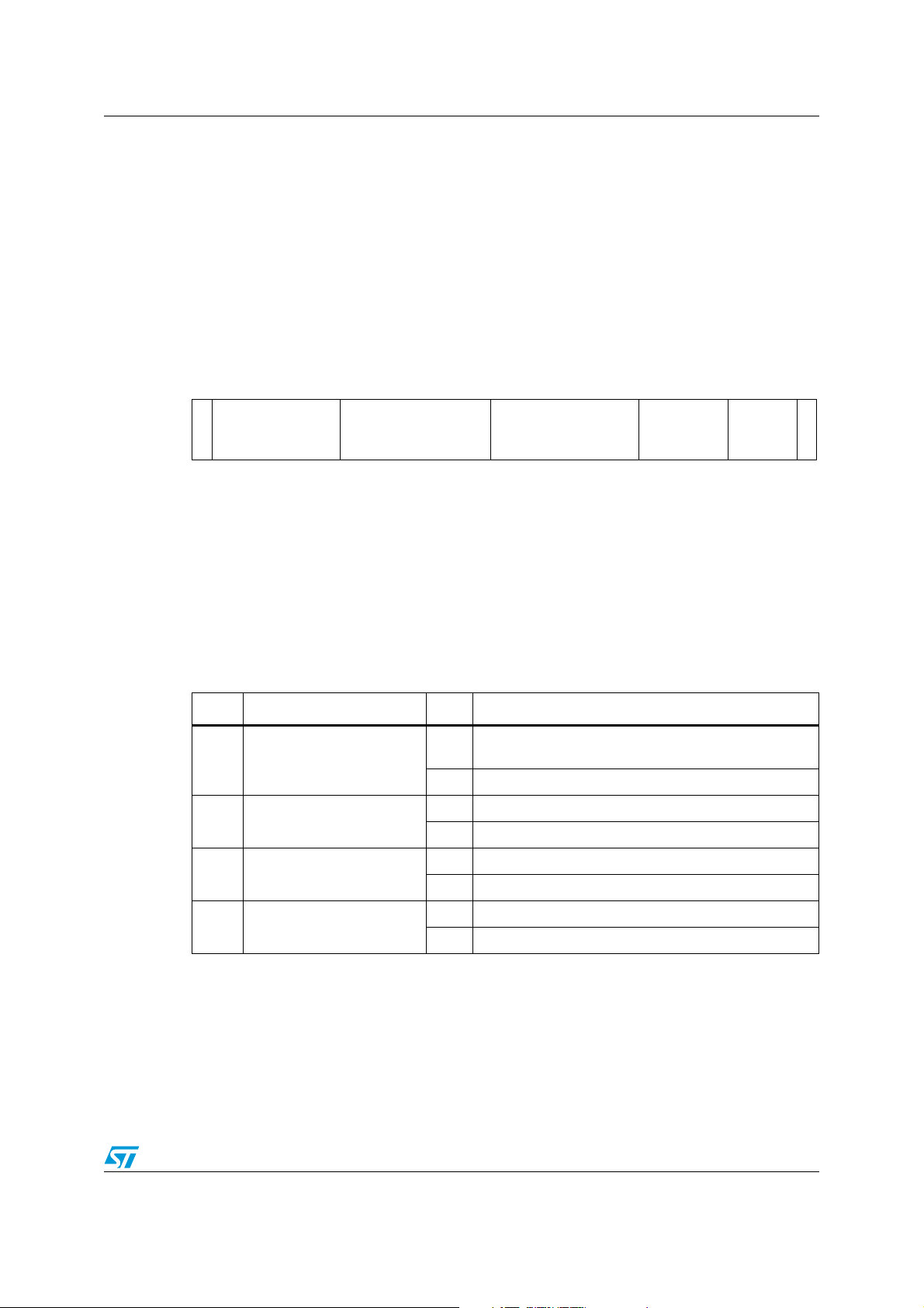
M24LR16E-R Request format
19 Request format
The request consists of:
● an SOF,
● flags,
● a command code,
● parameters and data,
● a CRC,
● an EOF.
Table 26. General request format
S
OFRequest_flags Command code Parameters Data CRCEO
F
19.1 Request flags
In a request, the “flags” field specifies the actions to be performed by the M24LR16E-R and
whether corresponding fields are present or not.
The flags field consists of eight bits. Bit 3 (Inventory_flag) of the request flag defines the
contents of the four MSBs (bits 5 to 8). When bit 3 is reset (0), bits 5 to 8 define the
M24LR16E-R selection criteria. When bit 3 is set (1), bits 5 to 8 define the M24LR16E-R
Inventory parameters.
Table 27. Definition of request flags 1 to 4
Bit No Flag Level Description
A single subcarrier frequency is used by the
Bit 1 Subcarrier_flag
Bit 2 Data_rate_flag
(1)
(2)
Bit 3 Inventory_flag
Bit 4 Protocol_extension_flag
1. Subcarrier_flag refers to the M24LR16E-R-to-VCD communication.
2. Data_rate_flag refers to the M24LR16E-R-to-VCD communication.
3. Protocol_extension_flag must be set to 1 for commands: Read Single Block, Read Multiple Block, Fast
Read Multiple Block, Write Single Block, Get Multiple Block Security Status. Command Get System Info
supports two options: a standard response format when Protocol_extension_flag is set to 0, and a rich
response when protocol extension is set to 1.
(3)
0
M24LR16E-R
1 Two subcarrier are used by the M24LR16E-R
0 Low data rate is used
1 High data rate is used
0 The meaning of flags 5 to 8 is described in Ta bl e 2 8
1 The meaning of flags 5 to 8 is described in Ta bl e 2 9
0 No Protocol format extension
1 Protocol format extension
Doc ID 018932 Rev 8 69/143
Page 70
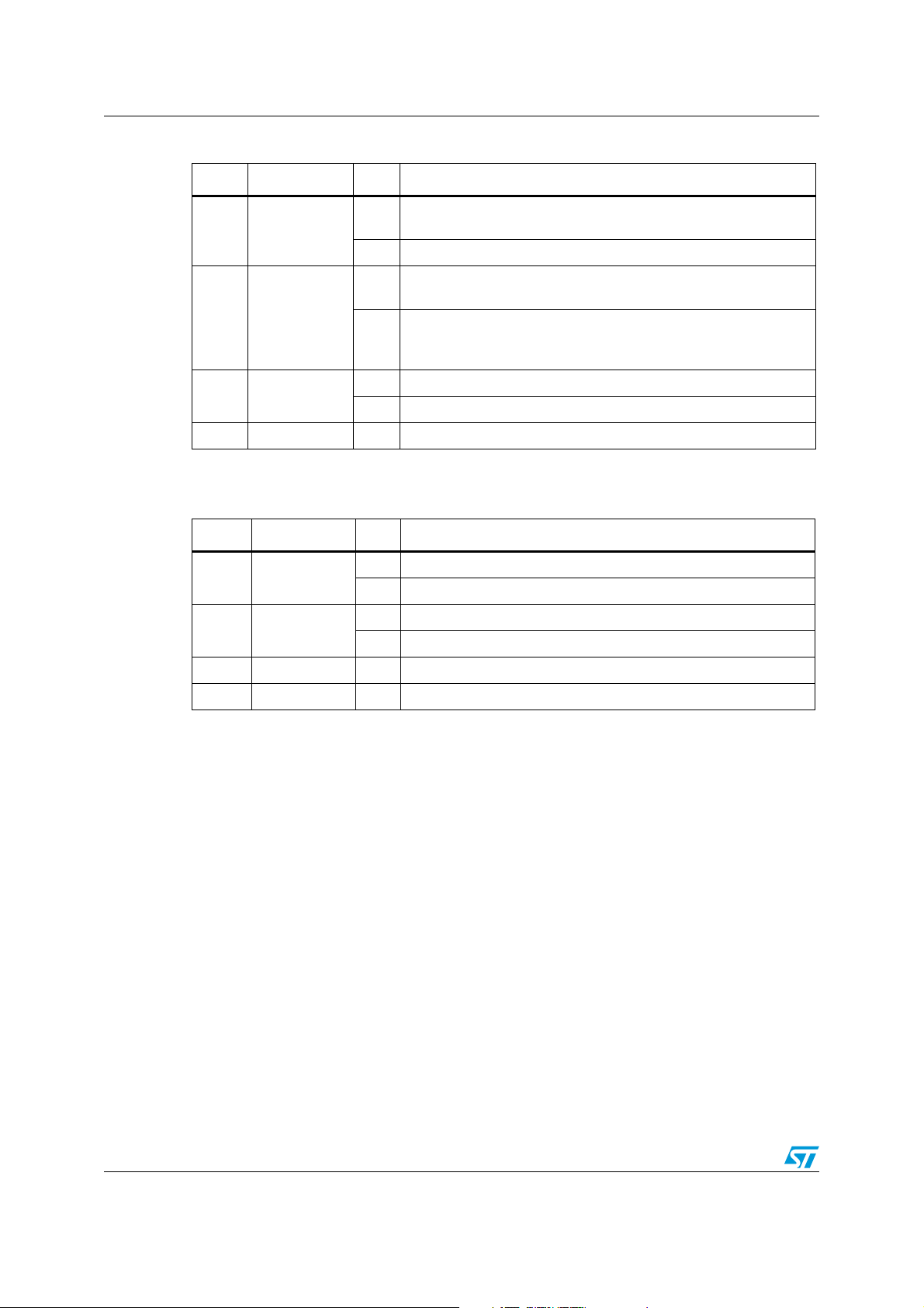
Request format M24LR16E-R
.
Table 28. Request flags 5 to 8 when Bit 3 = 0
Bit No Flag Level Description
Request is executed by any M24LR16E-R according to the setting
Bit 5 Select flag
(1)
Bit 6 Address flag
Bit 7 Option flag
Bit 8 RFU 0
1. If the Select_flag is set to 1, the Address_flag is set to 0 and the UID field is not present in the request.
Table 29. Request flags 5 to 8 when Bit 3 = 1
Bit No Flag Level Description
0
of Address_flag
1 Request is executed only by the M24LR16E-R in Selected state
Request is not addressed. UID field is not present. The request is
0
executed by all M24LR16E-Rs.
(1)
Request is addressed. UID field is present. The request is
1
executed only by the M24LR16E-R whose UID matches the UID
specified in the request.
0 Option not activated.
1 Option activated.
Bit 5 AFI flag
Bit 6 Nb_slots flag
Bit 7 Option flag 0
Bit 8 RFU 0
0 AFI field is not present
1 AFI field is present
0 16 slots
11 slot
70/143 Doc ID 018932 Rev 8
Page 71
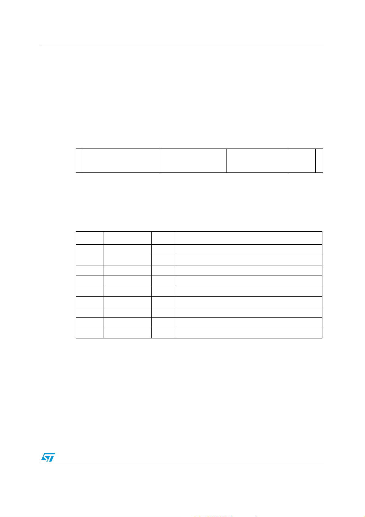
M24LR16E-R Response format
20 Response format
The response consists of:
● an SOF,
● flags,
● parameters and data,
● a CRC,
● an EOF.
Table 30. General response format
S
O
F
20.1 Response flags
In a response, the flags indicate how actions have been performed by the M24LR16E-R and
whether corresponding fields are present or not. The response flags consist of eight bits.
Table 31. Definitions of response flags 1 to 8
Response_flags Parameters Data CRCEO
F
Bit No Flag Level Description
0 No error
Bit 1 Error_flag
1 Error detected. Error code is in the “Error” field.
Bit 2 RFU 0
Bit 3 RFU 0
Bit 4 Extension flag 0 No extension
Bit 5 RFU 0
Bit 6 RFU 0
Bit 7 RFU 0
Bit 8 RFU 0
Doc ID 018932 Rev 8 71/143
Page 72
Response format M24LR16E-R
20.2 Response error code
If the Error_flag is set by the M24LR16E-R in the response, the Error code field is present
and provides information about the error that occurred.
Error codes not specified in Ta bl e 3 2 are reserved for future use.
Table 32. Response error code definition
Error code Meaning
03h The option is not supported.
0Fh Error with no information given.
10h The specified block is not available.
11h The specified block is already locked and thus cannot be locked again.
12h The specified block is locked and its contents cannot be changed.
13h The specified block was not successfully programmed.
14h The specified block was not successfully locked.
15h The specified block is read-protected.
72/143 Doc ID 018932 Rev 8
Page 73
M24LR16E-R Anticollision
21 Anticollision
The purpose of the anticollision sequence is to inventory the M24LR16E-Rs present in the
VCD field using their unique ID (UID).
The VCD is the master of communications with one or several M24LR16E-Rs. It initiates
M24LR16E-R communication by issuing the Inventory request.
The M24LR16E-R sends its response in the determined slot or does not respond.
21.1 Request parameters
When issuing the Inventory Command, the VCD:
● sets the Nb_slots_flag as desired,
● adds the mask length and the mask value after the command field.
● The mask length is the number of significant bits of the mask value.
● The mask value is contained in an integer number of bytes. The mask length indicates
the number of significant bits. LSB is transmitted first.
● If the mask length is not a multiple of 8 (bits), as many 0-bits as required are added to
the mask value MSB so that the mask value is contained in an integer number of bytes.
● The next field starts at the next byte boundary.
Table 33. Inventory request format
MSB LSB
SOF
Request_
flags
Command
Optional
AFI
Mask
length
Mask value CRC EOF
8 bits 8 bits 8 bits 8 bits 0 to 8 bytes 16 bits
In the example provided in Ta bl e 3 4 and Figure 50, the mask length is 11 bits. Five 0-bits are
added to the mask value MSB. The 11-bit mask and the current slot number are compared
to the UID.
Table 34. Example of the addition of 0-bits to an 11-bit mask value
(b15) MSB LSB (b0)
0000 0 100 1100 1111
0-bits added 11-bit mask value
Doc ID 018932 Rev 8 73/143
Page 74
Anticollision M24LR16E-R
AI06682
Mask value received in the Inventory command 0000 0100 1100 1111b16 bits
The Mask value less the padding 0s is loaded
into the Tag comparator
100 1100 1111b11 bits
The Slot counter is calculated
xxxxNb_slots_flags = 0 (16 slots), Slot Counter is 4 bits
The Slot counter is concatened to the Mask value
xxxx 100 1100 1111
b
Nb_slots_flags = 0 15 bits
The concatenated result is compared with
the least significant bits of the Tag UID.
xxxx xxxx ..... xxxx xxxx x xxx xxxx xxxx xxxx 64 bits
LSBMSB
b
LSBMSB
LSBMSB
LSBMSB
b0b63
CompareBits ignored
UID
4 bits
Figure 50. Principle of comparison between the mask, the slot number and the UID
The AFI field is present if the AFI_flag is set.
The pulse is generated according to the definition of the EOF in ISO/IEC 15693-2.
The first slot starts immediately after the request EOF is received. To switch to the next slot,
the VCD sends an EOF.
The following rules and restrictions apply:
● If no M24LR16E-R answer is detected, the VCD may switch to the next slot by sending
an EOF.
● If one or more M24LR16E-R answers are detected, the VCD waits until the complete
frame has been received before sending an EOF for switching to the next slot.
74/143 Doc ID 018932 Rev 8
Page 75

M24LR16E-R Request processing by the M24LR16E-R
22 Request processing by the M24LR16E-R
Upon reception of a valid request, the M24LR16E-R performs the following algorithm:
● NbS is the total number of slots (1 or 16)
● SN is the current slot number (0 to 15)
● LSB (value, n) function returns the n Less Significant Bits of value
● MSB (value, n) function returns the n Most Significant Bits of value
● “&” is the concatenation operator
● Slot_Frame is either an SOF or an EOF
SN = 0
if (Nb_slots_flag)
then NbS = 1
SN_length = 0
endif
else NbS = 16
SN_length = 4
endif
label1:
if LSB(UID, SN_length + Mask_length) =
LSB(SN,SN_length)&LSB(Mask,Mask_length)
then answer to inventory request
endif
wait (Slot_Frame)
if Slot_Frame = SOF
then Stop Anticollision
decode/process request
exit
endif
if Slot_Frame = EOF
if SN < NbS-1
then SN = SN + 1
goto label1
exit
endif
endif
Doc ID 018932 Rev 8 75/143
Page 76

Explanation of the possible cases M24LR16E-R
23 Explanation of the possible cases
Figure 51 summarizes the main possible cases that can occur during an anticollision
sequence when the number of slots is 16.
The sequence of steps is as follows:
● The VCD sends an Inventory request, in a frame terminated by an EOF. The number of
slots is 16.
● M24LR16E-R_1 transmits its response in Slot 0. It is the only one to do so, therefore no
collision occurs and its UID is received and registered by the VCD.
● The VCD sends an EOF in order to switch to the next slot.
● In Slot 1, two M24LR16E-Rs, M24LR16E-R_2 and M24LR16E-R_3 transmit a
response, thus generating a collision. The VCD records the event and registers that a
collision was detected in Slot 1.
● The VCD sends an EOF in order to switch to the next slot.
● In Slot 2, no M24LR16E-R transmits a response. Therefore the VCD does not detect
any M24LR16E-R SOF and switches to the next slot by sending an EOF.
● In Slot 3, another collision occurs due to responses from M24LR16E-R_4 and
M24LR16E-R_5.
● The VCD sends a request (for instance a Read Block) to M24LR16E-R_1 whose UID
has already been correctly received.
● All M24LR16E-Rs detect an SOF and exit the anticollision sequence. They process this
request and since the request is addressed to M24LR16E-R_1, only M24LR16E-R_1
transmits a response.
● All M24LR16E-Rs are ready to receive another request. If it is an Inventory command,
the slot numbering sequence restarts from 0.
Note: The decision to interrupt the anticollision sequence is made by the VCD. It could have
continued to send EOFs until Slot 16 and only then sent the request to M24LR16E-R_1.
76/143 Doc ID 018932 Rev 8
Page 77
Slot 0 Slot 1 Slot 2 Slot 3
M24LR16E-R Explanation of the possible cases
Figure 51. Description of a possible anticollision sequence
Doc ID 018932 Rev 8 77/143
VCD SOF
M24RF64s
Timing t1 t2 t1 t2 t3 t1 t2 t1
Comment
Time
Inventory
Request
EOF EOF EOF EOF SOF
Response
1
No
collision
Response
2
Response
3
Collision
No
Response
Response
4
Response
5
Collision
Request to
M24RF64_1
EOF
Response
from
M24RF64_1
AI15117
Page 78

Inventory Initiated command M24LR16E-R
24 Inventory Initiated command
The M24LR16E-R provides a special feature to improve the inventory time response of
moving tags using the Initiate_flag value. This flag, controlled by the Initiate command,
allows tags to answer to Inventory Initiated commands.
For applications in which multiple tags are moving in front of a reader, it is possible to miss
tags using the standard inventory command. The reason is that the inventory sequence has
to be performed on a global tree search. For example, a tag with a particular UID value may
have to wait the run of a long tree search before being inventoried. If the delay is too long,
the tag may be out of the field before it has been detected.
Using the Initiate command, the inventory sequence is optimized. When multiple tags are
moving in front of a reader, the ones which are within the reader field are initiated by the
Initiate command. In this case, a small batch of tags answers to the Inventory Initiated
command, which optimizes the time necessary to identify all the tags. When finished, the
reader has to issue a new Initiate command in order to initiate a new small batch of tags
which are new inside the reader field.
It is also possible to reduce the inventory sequence time using the Fast Initiate and Fast
Inventory Initiated commands. These commands allow the M24LR16E-Rs to increase their
response data rate by a factor of 2, up to 53 Kbit/s.
78/143 Doc ID 018932 Rev 8
Page 79
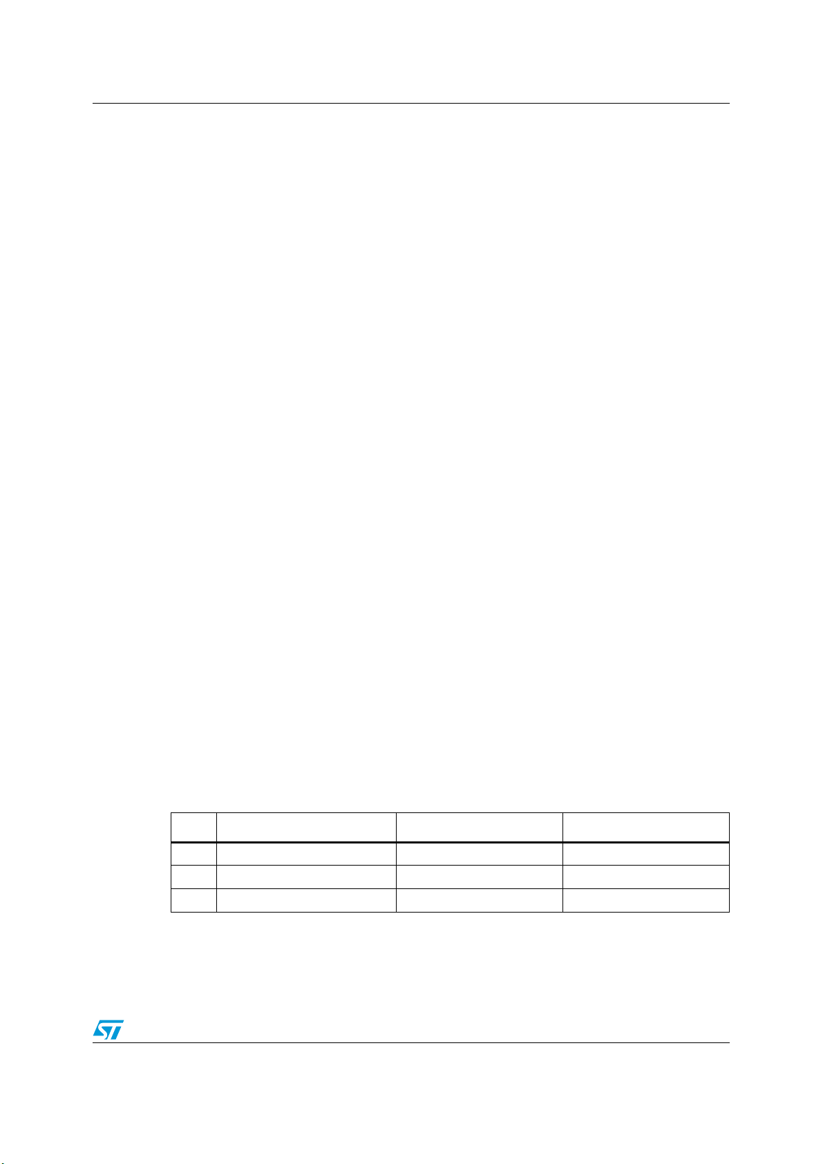
M24LR16E-R Timing definition
25 Timing definition
25.1 t1: M24LR16E-R response delay
Upon detection of the rising edge of the EOF received from the VCD, the M24LR16E-R
waits for a time t
next slot during an inventory process. Values of t
in Figure 22.
25.2 t2: VCD new request delay
t2 is the time after which the VCD may send an EOF to switch to the next slot when one or
more M24LR16E-R responses have been received during an Inventory command. It starts
from the reception of the EOF from the M24LR16E-Rs.
The EOF sent by the VCD may be either 10% or 100% modulated regardless of the
modulation index used for transmitting the VCD request to the M24LR16E-R.
t
is also the time after which the VCD may send a new request to the M24LR16E-R, as
2
described in Figure 48.
before transmitting its response to a VCD request or switching to the
1nom
are given in Tab l e 3 5. The EOF is defined
1
Values of t
are given in Ta bl e 3 5 .
2
25.3 t3: VCD new request delay when no response is received from the M24LR16E-R
t3 is the time after which the VCD may send an EOF to switch to the next slot when no
M24LR16E-R response has been received.
The EOF sent by the VCD may be either 10% or 100% modulated regardless of the
modulation index used for transmitting the VCD request to the M24LR16E-R.
From the time the VCD has generated the rising edge of an EOF:
● If this EOF is 100% modulated, the VCD waits for a time at least equal to t
sending a new EOF.
● If this EOF is 10% modulated, the VCD waits for a time at least equal to the sum of t
+ the M24LR16E-R nominal response time (which depends on the M24LR16E-R data
rate and subcarrier modulation mode) before sending a new EOF.
Table 35. Timing values
Minimum (min) values Nominal (nom) values Maximum (max) values
t
1
t
2
t
3
1. The tolerance of specific timings is ± 32/fC.
2. t
does not apply for write-alike requests. Timing conditions for write-alike requests are defined in the
1max
command description.
is the time taken by the M24LR16E-R to transmit an SOF to the VCD. t
3. t
SOF
data rate: High data rate or Low data rate.
318.6 µs 320.9 µs 323.3 µs
309.2 µs No t
(2)
t
+ t
1max
SOF
(3)
(1)
No t
nom
nom
No t
No t
depends on the current
SOF
3min
max
max
before
3min
Doc ID 018932 Rev 8 79/143
Page 80
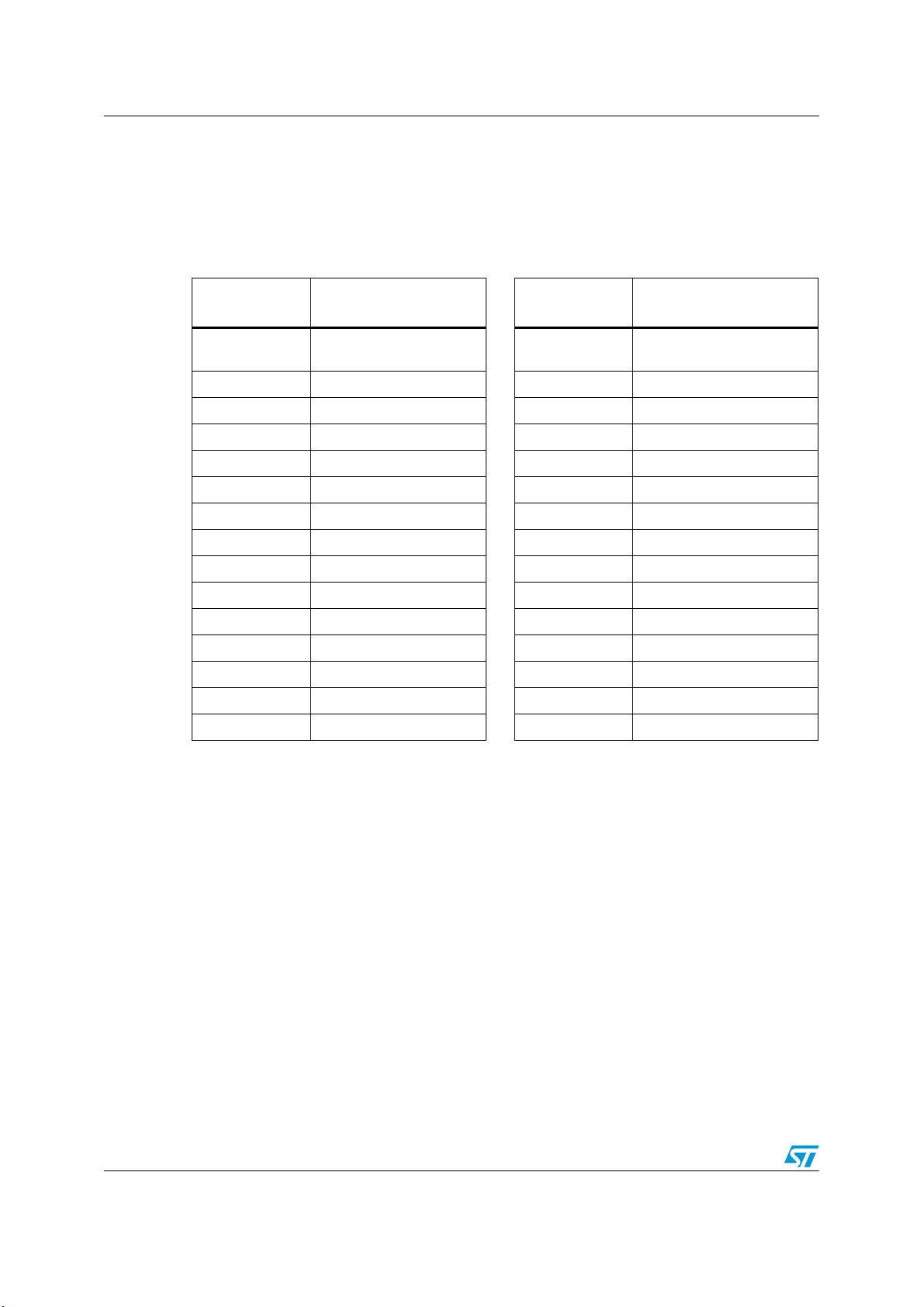
Command codes M24LR16E-R
26 Command codes
The M24LR16E-R supports the commands described in this section. Their codes are given
in Ta bl e 3 6 .
Table 36. Command codes
Command code
standard
01h Inventory 2Ch
02h Stay Quiet B1h Write-sector Password
20h Read Single Block B2h Lock-sector
21h Write Single Block B3h Present-sector Password
23h Read Multiple Block C0h Fast Read Single Block
25h Select C1h Fast Inventory Initiated
26h Reset to Ready C2h Fast Initiate
27h Write AFI C3h Fast Read Multiple Block
28h Lock AFI D1h Inventory Initiated
29h Write DSFID D2h Initiate
2Ah Lock DSFID A0h ReadCfg
2Bh Get System Info A1h WriteEHCfg
Function
Command code
custom
Get Multiple Block Security
Status
A2h SetRstEHEn
A3h CheckEHEn
A4h WriteDOCfg
Function
80/143 Doc ID 018932 Rev 8
Page 81
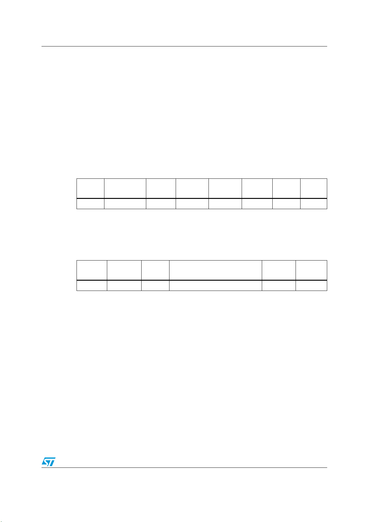
M24LR16E-R Command codes
26.1 Inventory
When receiving the Inventory request, the M24LR16E-R runs the anticollision sequence.
The Inventory_flag is set to 1. The meaning of flags 5 to 8 is shown in Ta b le 2 9 .
The request contains:
● the flags,
● the Inventory command code (see Tab le 3 6 ),
● the AFI if the AFI flag is set,
● the mask length,
● the mask value,
● the CRC.
The M24LR16E-R does not generate any answer in case of error.
Table 37. Inventory request format
Request
SOF
Request_flags Inventory
Optional
AFI
Mask
length
Mask
value
CRC16
Request
EOF
8 bits 01h 8 bits 8 bits 0 - 64 bits 16 bits
The response contains:
● the flags,
● the Unique ID.
Table 38. Inventory response format
Response
SOF
Response_
flags
DSFID UID CRC16
Response
EOF
8 bits 8 bits 64 bits 16 bits
During an Inventory process, if the VCD does not receive an RF M24LR16E-R response, it
waits for a time t
before sending an EOF to switch to the next slot. t3 starts from the rising
3
edge of the request EOF sent by the VCD.
● If the VCD sends a 100% modulated EOF, the minimum value of t
t
min = 4384/fC (323.3µs) + t
3
●
If the VCD sends a 10% modulated EOF, the minimum value of t3 is:
t
min = 4384/fC (323.3µs) + t
3
SOF
NRT
3
is:
where:
● t
● t
t
NRT
is the time required by the M24LR16E-R to transmit an SOF to the VCD,
SOF
is the nominal response time of the M24LR16E-R.
NRT
and t
are dependent on the M24LR16E-R-to-VCD data rate and subcarrier
SOF
modulation mode.
When configured in the RF busy mode, the RF WIP/BUSY pin is tied to 0 from the SOF
starting the inventory command to the end of the M24LR16E-R response. If the M24LR16ER does not receive the corresponding slot marker, the RF WIP/BUSY pin remains at 0 until
the next RF power-off.
Doc ID 018932 Rev 8 81/143
Page 82
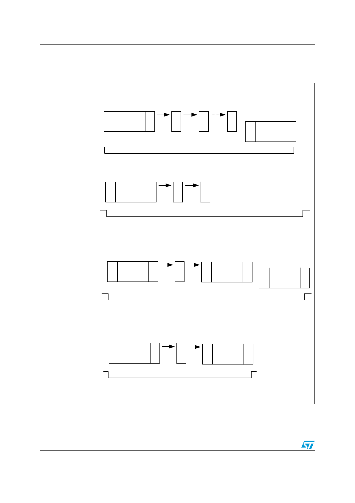
Command codes M24LR16E-R
MS19754V1
S
O
F
Inventory
command
E
O
F
E
O
F
Slot 1
S
O
F
Ireply
M24LR16
E
O
F
E
O
F
E
O
F
Slot n
1) M24LR16 replies in slot n. RF_Busy is released after M24LR16 response.
RF_Busy
S
O
F
Inventory
command
E
O
F
E
O
F
Slot 1
E
O
F
Slot n
2) Slot n never occurs. RF_Busy is only released by Power-off.
Power-off
RF_Busy
S
O
F
Inventory
command
E
O
F
E
O
F
Slot 1
3) VCD sends a Valid command before slot n. RF_Busy is released after M24LR16
response.
RF_Busy
S
O
F
Inventory
command
E
O
F
E
O
F
Slot 1
4) VCD sends a Bad command before slot n. RF_Busy is released after VCD
command.
RF_Busy
S
O
F
INew
command
E
O
F
S
O
F
Ireply
M24LR16
E
O
F
S
O
F
INew
command
E
O
F
When configured in the RF write in progress mode, the RF WIP/BUSY pin remains in high-Z
state.
Figure 52. M24LR16 RF-Busy management following Inventory command
82/143 Doc ID 018932 Rev 8
Page 83
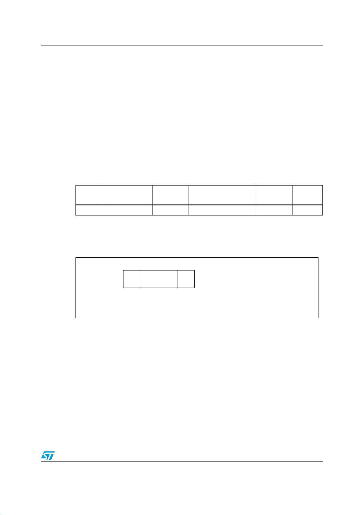
M24LR16E-R Command codes
26.2 Stay Quiet
Command code = 0x02
On receiving the Stay Quiet command, the M24LR16E-R enters the Quiet State if no error
occurs, and does NOT send back a response. There is NO response to the Stay Quiet
command even if an error occurs.
When in the Quiet state:
● the M24LR16E-R does not process any request if the Inventory_flag is set,
● the M24LR16E-R processes any Addressed request.
The M24LR16E-R exits the Quiet State when:
● it is reset (power off),
● receiving a Select request. It then goes to the Selected state,
● receiving a Reset to Ready request. It then goes to the Ready state.
Table 39. Stay Quiet request format
Request
SOF
Request flags Stay Quiet UID CRC16
8 bits 02h 64 bits 16 bits
Request
EOF
The Stay Quiet command must always be executed in Addressed mode (Select_flag is reset
to 0 and Address_flag is set to 1).
Figure 53. Stay Quiet frame exchange between VCD and M24LR16E-R
VCD SOF
M24LR16E-R
Timing
Stay Quiet
request
EOF
When configured in the RF busy mode, the RF WIP/BUSY pin is tied to 0 during the Stay
Quiet command.
When configured in the RF write in progress mode, the RF WIP/BUSY pin remains in high-Z
state.
Doc ID 018932 Rev 8 83/143
Page 84
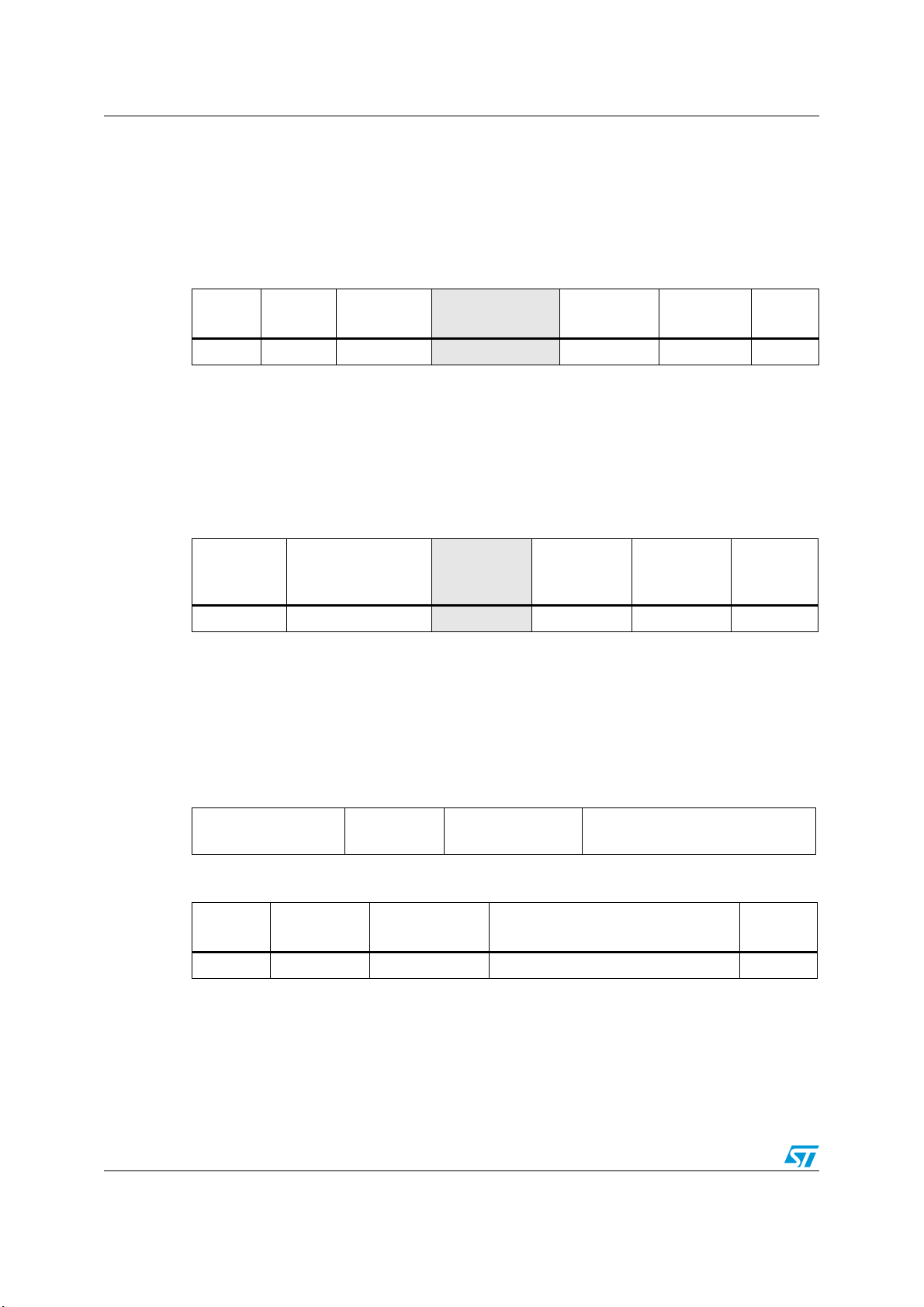
Command codes M24LR16E-R
26.3 Read Single Block
On receiving the Read Single Block command, the M24LR16E-R reads the requested block
and sends back its 32-bit value in the response. The Protocol_extension_flag should be set
to 1 for the M24LR16E-R to operate correctly. If the Protocol_extension_flag is at 0, the
M24LR16E-R answers with an error code. The Option_flag is supported.
Table 40. Read Single Block request format
Request
SOF
1. Gray means that the field is optional.
Request_
Read Single
flags
8 bits 20h
Block
UID
(1)
Block
number
CRC16
64 bits 16 bits 16 bits
Request parameters:
● Request flags
● UID (optional)
● Block number
Table 41. Read Single Block response format when Error_flag is NOT set
Response
SOF
Response_flags
8 bits
1. Gray means that the field is optional.
Sector
security
(1)
status
Data CRC16
8 bits 32 bits 16 bits
Response parameters:
● Sector security status if Option_flag is set (see Ta b l e 4 2 )
● Four bytes of block data
Table 42. Sector security status
b
Reserved for future
b
7
6
use. All at 0.
b
5
b
b
4
Password
control bits
3
b
2
Read / Write
protection bits
b
1
0: Current sector not locked
1: Current sector locked
b
0
Request
EOF
Response
EOF
Table 43. Read Single Block response format when Error_flag is set
Response
SOF
Response_
flags
Error code CRC16
8 bits 8 bits 16 bits
Response parameter:
● Error code as Error_flag is set
– 10h: the specified block is not available
– 15h: the specified block is read-protected
84/143 Doc ID 018932 Rev 8
Response
EOF
Page 85
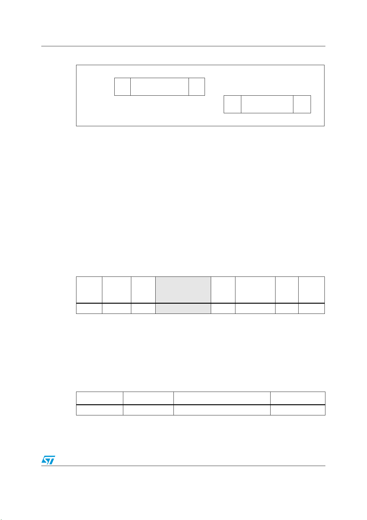
M24LR16E-R Command codes
Figure 54. Read Single Block frame exchange between VCD and M24LR16E-R
VCD SOF
Read Single Block
M24LR16E-R <-t
When configured in the RF busy mode, the RF WIP/BUSY pin is tied to 0 from the SOF that
starts the Read Single Block command to the end of the M24LR16E-R response.
When configured in the RF write in progress mode, the RF WIP/BUSY pin remains in high-Z
state.
26.4 Write Single Block
On receiving the Write Single Block command, the M24LR16E-R writes the data contained
in the request to the requested block and reports whether the write operation was
successful in the response. The Protocol_extension_flag should be set to 1 for the
M24LR16E-R to operate correctly. If the Protocol_extension_flag is at 0, the M24LR16E-R
answers with an error code. The Option_flag is supported.
During the RF write cycle W
otherwise, the M24LR16E-R may not program correctly the data into the memory. The W
time is equal to t
Table 44. Write Single Block request format
+ 18 × 302 µs.
1nom
request
, there should be no modulation (neither 100% nor 10%),
t
EOF
-> SOF
1
Read Single Block
response
EOF
t
Request
SOF
Request_
flags
8 bits 21h
1. Gray means that the field is optional.
Write
Single
Block
UID
(1)
Block
number
Data CRC16
64 bits 16 bits 32 bits 16 bits
Request
Request parameters:
● Request flags
● UID (optional)
● Block number
● Data
Table 45. Write Single Block response format when Error_flag is NOT set
Response SOF Response_flags CRC16 Response EOF
8 bits 16 bits
Response parameter:
● No parameter. The response is send back after the writing cycle.
EOF
Doc ID 018932 Rev 8 85/143
Page 86
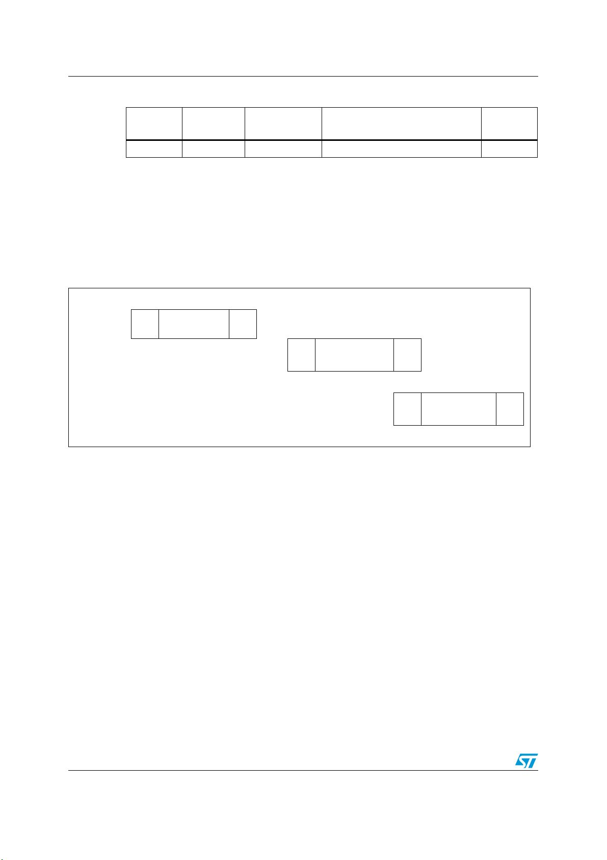
Command codes M24LR16E-R
Table 46. Write Single Block response format when Error_flag is set
Response
SOF
Response_
flags
Error code CRC16
8 bits 8 bits 16 bits
Response parameter:
● Error code as Error_flag is set:
– 0Fh: error with no information given
– 10h: the specified block is not available
– 12h: the specified block is locked and its contents cannot be changed
– 13h: the specified block was not successfully programmed
Figure 55. Write Single Block frame exchange between VCD and M24LR16E-R
VCD SOF
M24LR16E-
M24LR16E-
Write Single
Block request
R
R
EOF
<-t
1
<------------------- W
-> SOF
Write Single
Block response
---------------> SOF
t
EOF
Write sequence when
Write Single
Block response
Response
EOF
error
EOF
When configured in the RF busy mode, the RF WIP/BUSY pin is tied to 0 from the SOF that
starts the Write Single Block command to the end of the M24LR16E-R response.
When configured in the RF write in progress mode, the RF WIP/BUSY pin is tied to 0 for the
duration of the internal write cycle (from the end of a valid write single block command to the
beginning of the M24LR16E-R response).
86/143 Doc ID 018932 Rev 8
Page 87
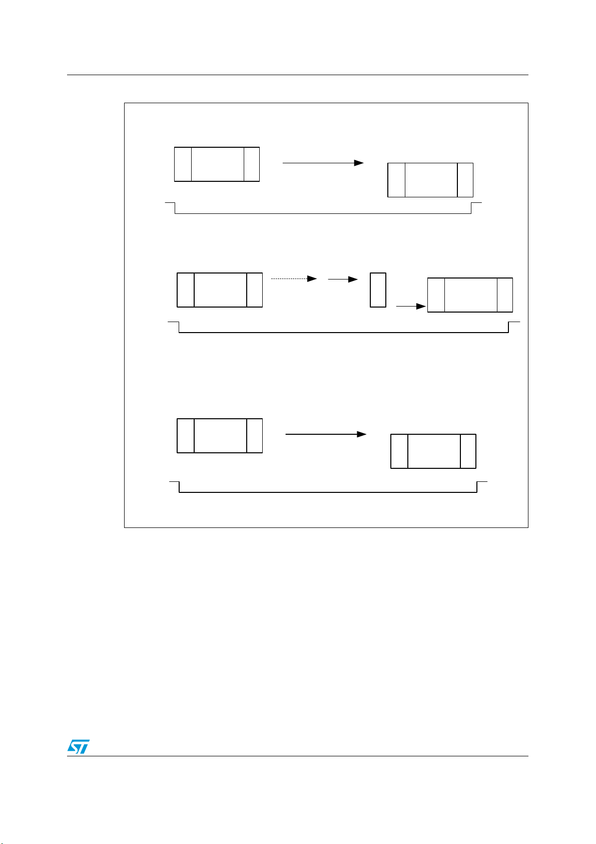
M24LR16E-R Command codes
MS19756V1
S
O
F
Write
command
E
O
F
S
O
F
Ireply
M24LR16
E
O
F
1) M24LR16 replies. RF_Busy is released after M24LR16 response.
RF_Busy
S
O
F
Write
command
E
O
F
E
O
F
2) M24LR16 replies when option flag is set. RF_Busy is released after M24LR16
response.
RF_Busy
Wt
Wt
t1
S
O
F
Ireply
M24LR16
E
O
F
3) VCD sends a forbidden Write (sector lock, password-protected). RF_Busy is
released after M24LR16 command.
S
O
F
Write
command
E
O
F
S
O
F
Ireply
M24LR16
E
O
F
t1
RF_Busy
Figure 56. M24LR16 RF-Busy management following Write command
Doc ID 018932 Rev 8 87/143
Page 88
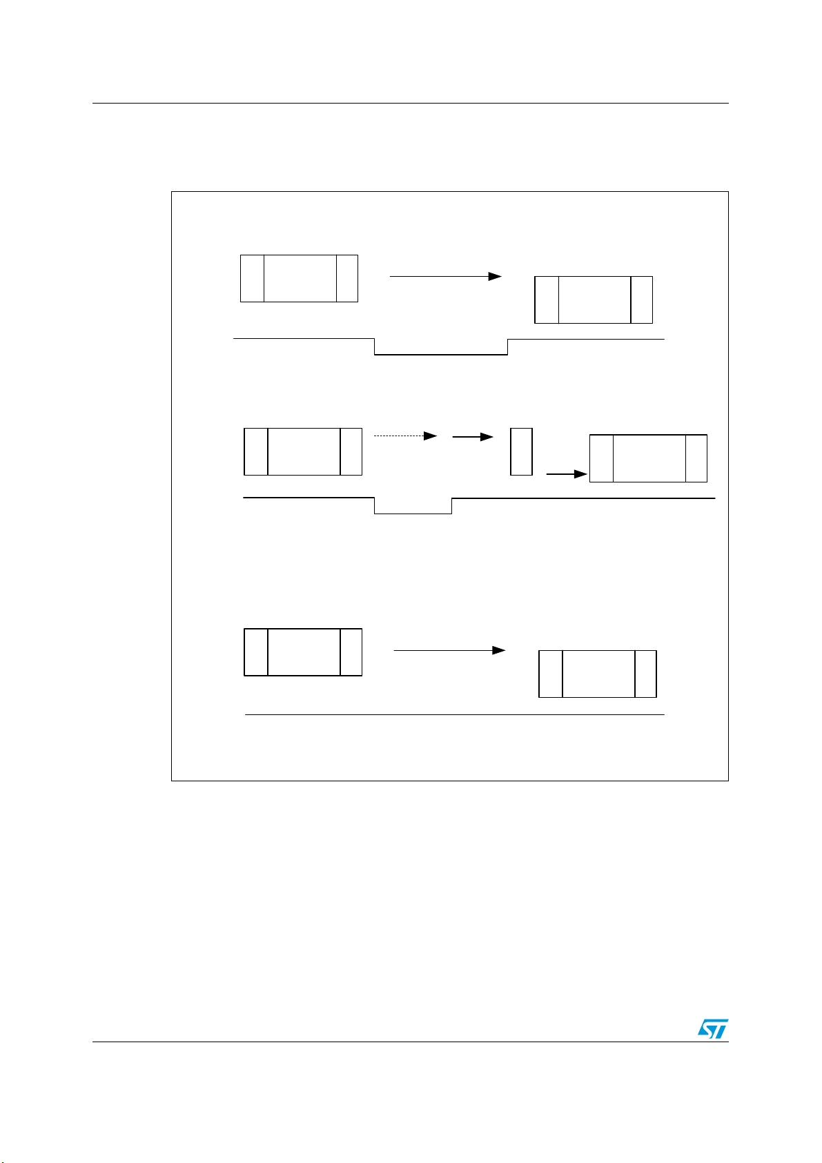
Command codes M24LR16E-R
MS19762V1
S
O
F
Write
command
E
O
F
S
O
F
Ireply
M24LR16
E
O
F
1) M24LR16 replies. RF_Wip is released after M24LR16 response.
RF_Wip
S
O
F
Write
command
E
O
F
E
O
F
2) M24LR16 replies when option flag is set. RF_Wip is released after M24LR16
response.
RF_Wip
Wt
Wt
t1
S
O
F
Ireply
M24LR16
E
O
F
3) VCD sends a forbidden Write (sector lock, password-protected). RF_Wip is
released after M24LR16 command.
S
O
F
Write
command
E
O
F
S
O
F
Ireply
M24LR16
E
O
F
t1
RF_Wip
When configuring in the RF Write in progress mode, the RF WIP/BUSY pin is tied to 0
during the Write & verify sequence, as shown in Figure 57.
Figure 57. M24LR16 RF-Wip management following Write command
88/143 Doc ID 018932 Rev 8
Page 89
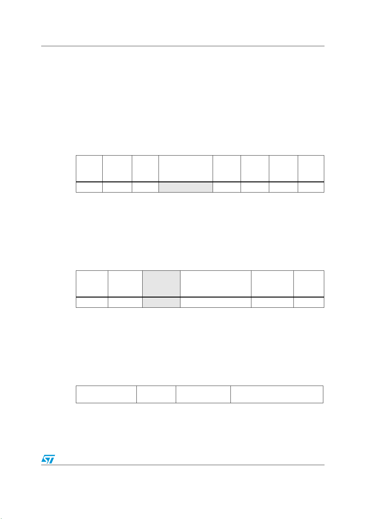
M24LR16E-R Command codes
26.5 Read Multiple Block
When receiving the Read Multiple Block command, the M24LR16E-R reads the selected
blocks and sends back their value in multiples of 32 bits in the response. The blocks are
numbered from 00h to 1FFh in the request and the value is minus one (–1) in the field. For
example, if the “Number of blocks” field contains the value 06h, seven blocks are read. The
maximum number of blocks is fixed at 32 assuming that they are all located in the same
sector. If the number of blocks overlaps sectors, the M24LR16E-R returns an error code.
The Protocol_extension_flag should be set to 1 for the M24LR16E-R to operate correctly. If
the Protocol_extension_flag is at 0, the M24LR16E-R answers with an error code. The
Option_flag is supported.
Table 47. Read Multiple Block request format
Request
SOF
Request_
flags
Read
Multiple
Block
8 bits 23h
1. Gray means that the field is optional.
(1)
UID
64 bits 16 bits 8 bits 16 bits
First
block
number
Number
of blocks
CRC16
Request parameters:
● Request flags
● UID (optional)
● First block number
● Number of blocks
Table 48. Read Multiple Block response format when Error_flag is NOT set
Response
SOF
Response_
flags
8 bits
1. Gray means that the field is optional.
2. Repeated as needed.
Sector
security
(1)
status
(2)
8 bits
Data CRC16
(2)
32 bits
16 bits
Response parameters:
● Sector security status if Option_flag is set (see Ta b l e 4 9 )
● N blocks of data
Table 49. Sector security status
b
Reserved for future
b
7
6
use. All at 0.
b
5
b
b
4
Password
control bits
3
b
2
Read / Write
protection bits
b
1
0: Current sector not locked
1: Current sector locked
b
0
Request
EOF
Response
EOF
Doc ID 018932 Rev 8 89/143
Page 90
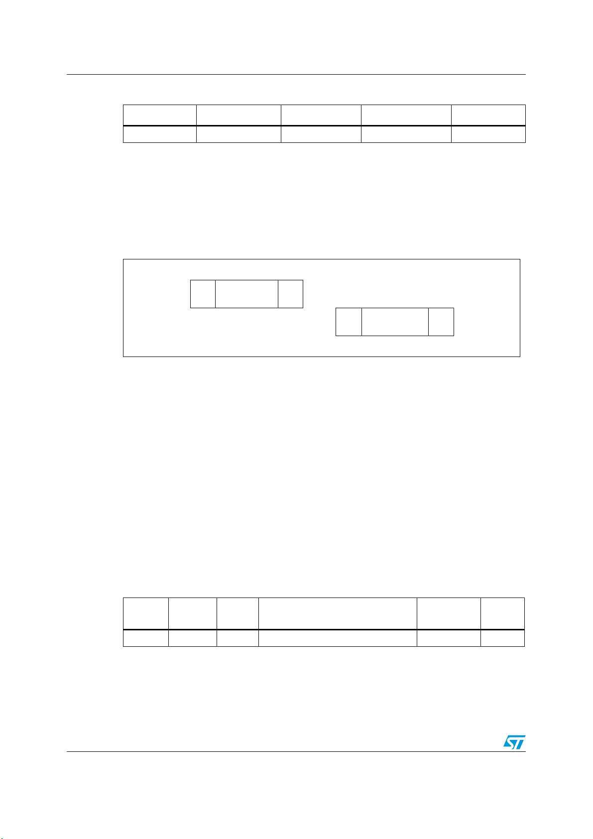
Command codes M24LR16E-R
Table 50. Read Multiple Block response format when Error_flag is set
Response SOF Response_flags Error code CRC16 Response EOF
8 bits 8 bits 16 bits
Response parameter:
● Error code as Error_flag is set:
– 0Fh: error with no information given
– 10h: the specified block is not available
– 15h: the specified block is read-protected
Figure 58. Read Multiple Block frame exchange between VCD and M24LR16E-R
VCD SOF
M24LR16E-R <-t
When configured in the RF busy mode, the RF WIP/BUSY pin is tied to 0 from the SOF that
starts the Read Multiple Block command to the end of the M24LR16E-R response.
When configured in the RF write in progress mode, the RF WIP/BUSY pin remains in high-Z
state.
26.6 Select
When receiving the Select command:
● If the UID is equal to its own UID, the M24LR16E-R enters or stays in the Selected
state and sends a response.
● If the UID does not match its own, the selected M24LR16E-R returns to the Ready
state and does not send a response.
The M24LR16E-R answers an error code only if the UID is equal to its own UID. If not, no
response is generated. If an error occurs, the M24LR16E-R remains in its current state.
Table 51. Select request format
Read Multiple
Block request
EOF
-> SOF
1
Read Multiple
Block response
EOF
Request
SOF
Request_
flags
8 bits 25h 64 bits 16 bits
Select UID CRC16
Request parameter:
● UID
90/143 Doc ID 018932 Rev 8
Request
EOF
Page 91
M24LR16E-R Command codes
Table 52. Select Block response format when Error_flag is NOT set
Response
SOF
Response_flags CRC16
8 bits 16 bits
Response parameter:
● No parameter
Table 53. Select response format when Error_flag is set
Response
SOF
Response_
flags
Error code CRC16
8 bits 8 bits 16 bits
Response parameter:
● Error code as Error_flag is set:
– 03h: the option is not supported
Figure 59. Select frame exchange between VCD and M24LR16E-R
VCD SOF
Select
request
EOF
Response
EOF
Response
EOF
M24LR16E-R <-t
-> SOF
1
Select
response
EOF
When configured in the RF busy mode, the RF WIP/BUSY pin is tied to 0 from the SOF that
starts the Select command to the end of the M24LR16E-R response.
When configured in the RF write in progress mode, the RF WIP/BUSY pin remains in high-Z
state.
Doc ID 018932 Rev 8 91/143
Page 92
Command codes M24LR16E-R
26.7 Reset to Ready
On receiving a Reset to Ready command, the M24LR16E-R returns to the Ready state if no
error occurs. In the Addressed mode, the M24LR16E-R answers an error code only if the
UID is equal to its own UID. If not, no response is generated.
Table 54. Reset to Ready request format
Request
SOF
Request_
flags
Reset to
Ready
UID
(1)
CRC16
8 bits 26h 64 bits 16 bits
1. Gray means that the field is optional.
Request parameter:
● UID (optional)
Table 55. Reset to Ready response format when Error_flag is NOT set
Response
SOF
Response_flags CRC16
8 bits 16 bits
Response parameter:
● No parameter
Table 56. Reset to ready response format when Error_flag is set
Response
SOF
Response_flags Error code CRC16
8 bits 8 bits 16 bits
Request
EOF
Response
EOF
Response
EOF
Response parameter:
● Error code as Error_flag is set:
– 03h: the option is not supported
Figure 60. Reset to Ready frame exchange between VCD and M24LR16E-R
Reset to
VCD SOF
M24LR16E-R <-t
92/143 Doc ID 018932 Rev 8
Ready
request
EOF
-> SOF
1
Reset to
Ready
response
EOF
Page 93
M24LR16E-R Command codes
When configured in the RF busy mode, the RF WIP/BUSY pin is tied to 0 from the SOF that
starts the Reset to ready command to the end of the M24LR16E-R response.
When configured in the RF write in progress mode, the RF WIP/BUSY pin remains in high-Z
state.
26.8 Write AFI
On receiving the Write AFI request, the M24LR16E-R programs the 8-bit AFI value to its
memory. The Option_flag is supported.
During the RF write cycle W
, there should be no modulation (neither 100% nor 10%),
t
otherwise, the M24LR16E-R may not write correctly the AFI value into the memory. The W
time is equal to t
Table 57. Write AFI request format
Request
SOF
1. Gray means that the field is optional.
Request
_flags
8 bits 27h 64 bits 8 bits 16 bits
+ 18 × 302 µs.
1nom
Write
AFI
UID
(1)
AFI CRC16
Request
EOF
Request parameter:
● Request flags
● UID (optional)
● AFI
Table 58. Write AFI response format when Error_flag is NOT set
Response
SOF
Response_flags CRC16
Response
EOF
8 bits 16 bits
Response parameter:
● No parameter
Table 59. Write AFI response format when Error_flag is set
t
Response
SOF
Response_
flags
Error code CRC16
8 bits 8 bits 16 bits
Response parameter:
● Error code as Error_flag is set
– 12h: the specified block is locked and its contents cannot be changed
– 13h: the specified block was not successfully programmed
Doc ID 018932 Rev 8 93/143
Response
EOF
Page 94
Command codes M24LR16E-R
Figure 61. Write AFI frame exchange between VCD and M24LR16E-R
VCD SOF
M24LR16E-R <-t
M24LR16E-R <------------------ Wt --------------> SOF
When configured in the RF busy mode, the RF WIP/BUSY pin is tied to 0 from the SOF that
starts the Write AFI command to the end of the M24LR16E-R response.
When configured in the RF write in progress mode, the RF WIP/BUSY pin is tied to 0 for the
duration of the internal write cycle (from the end of a valid Write AFI command to the
beginning of the M24LR16E-R response).
26.9 Lock AFI
On receiving the Lock AFI request, the M24LR16E-R locks the AFI value permanently. The
Option_flag is supported.
During the RF write cycle W
otherwise, the M24LR16E-R may not Lock correctly the AFI value in memory. The W
equal to t
Table 60. Lock AFI request format
1nom
Write AFI
request
+ 18 × 302 µs.
EOF
-> SOF
1
Write AFI
response
Write sequence
EOF
when error
Write AFI
response
, there should be no modulation (neither 100% nor 10%),
t
t
EOF
time is
Request
SOF
1. Gray means that the field is optional.
Request_
flags
8 bits 28h
Lock
AFI
(1)
UID
64 bits 16 bits
Request parameter:
● Request Flags
● UID (optional)
Table 61. Lock AFI response format when Error_flag is NOT set
Response
SOF
Response_flags CRC16
8 bits 16 bits
Response parameter:
● No parameter
94/143 Doc ID 018932 Rev 8
CRC16
Request
EOF
Response
EOF
Page 95
M24LR16E-R Command codes
Table 62. Lock AFI response format when Error_flag is set
Response
SOF
Response_flags Error code CRC16
8 bits 8 bits 16 bits
Response parameter:
● Error code as Error_flag is set
– 11h: the specified block is already locked and thus cannot be locked again
– 14h: the specified block was not successfully locked
Figure 62. Lock AFI frame exchange between VCD and M24LR16E-R
VCD SOF
M24LR16E-R <-t
M24LR16E-R
Lock AFI
request
EOF
<----------------- W
-> SOF
1
Lock AFI
response
-------------
t
>
EOF
SOF
Response
EOF
Lock sequence
when error
Lock AFI
response
EOF
When configured in the RF busy mode, the RF WIP/BUSY pin is tied to 0 from the SOF that
starts the Lock AFI command to the end of the M24LR16E-R response.
When configured in the RF write in progress mode, the RF WIP/BUSY pin is tied to 0 for the
entire duration of the internal write cycle (from the end of valid Lock AFI command to the
beginning of the M24LR16E-R response).
Doc ID 018932 Rev 8 95/143
Page 96
Command codes M24LR16E-R
26.10 Write DSFID
On receiving the Write DSFID request, the M24LR16E-R programs the 8-bit DSFID value to
its memory. The Option_flag is supported.
During the RF write cycle W
, there should be no modulation (neither 100% nor 10%),
t
otherwise, the M24LR16E-R may not write correctly the DSFID value in memory. The W
time is equal to t
Table 63. Write DSFID request format
Request
SOF
1. Gray means that the field is optional.
Request_
flags
8 bits 29h 64 bits 8 bits 16 bits
+ 18 × 302 µs.
1nom
Write
DSFID
UID
(1)
DSFID CRC16
Request
EOF
Request parameter:
● Request flags
● UID (optional)
● DSFID
Table 64. Write DSFID response format when Error_flag is NOT set
Response
SOF
Response_flags CRC16
Response
EOF
8 bits 16 bits
Response parameter:
● No parameter
Table 65. Write DSFID response format when Error_flag is set
t
Response
SOF
Response_flags Error code CRC16
8 bits 8 bits 16 bits
Response parameter:
● Error code as Error_flag is set
– 12h: the specified block is locked and its contents cannot be changed
– 13h: the specified block was not successfully programmed
96/143 Doc ID 018932 Rev 8
Response
EOF
Page 97
M24LR16E-R Command codes
Figure 63. Write DSFID frame exchange between VCD and M24LR16E-R
VCD SOF
M24LR16E-R <-t
M24LR16E-R
When configured in the RF busy mode, the RF WIP/BUSY pin is tied to 0 from the SOF that
starts the Write DSFID command to the end of the M24LR16E-R response.
When configured in the RF write in progress mode, the RF WIP/BUSY pin is tied to 0 for the
duration of the internal write cycle (from the end of a valid Write DSFID command to
beginning of the M24LR16E-R response).
26.11 Lock DSFID
On receiving the Lock DSFID request, the M24LR16E-R locks the DSFID value
permanently. The Option_flag is supported.
During the RF write cycle W
otherwise, the M24LR16E-R may not lock correctly the DSFID value in memory. The W
is equal to t
Table 66. Lock DSFID request format
1nom
Write DSFID
request
, there should be no modulation (neither 100% nor 10%),
t
+ 18 × 302 µs.
EO
F
1
<---------------- W
SOFWrite DSFID
->
response
EOFWrite sequence
when error
------------>SOFWrite DSFID
t
response
EOF
time
t
Request
SOF
1. Gray means that the field is optional.
Request_
flags
8 bits 2Ah
Lock
DSFID
(1)
UID
CRC16
64 bits 16 bits
Request parameter:
● Request flags
● UID (optional)
Table 67. Lock DSFID response format when Error_flag is NOT set
Response
SOF
Response_flags CRC16
8 bits 16 bits
Doc ID 018932 Rev 8 97/143
Request
EOF
Response
EOF
Page 98
Command codes M24LR16E-R
Response parameter:
● No parameter.
Table 68. Lock DSFID response format when Error_flag is set
Response
SOF
Response_flags Error code CRC16
8 bits 8 bits 16 bits
Response parameter:
● Error code as Error_flag is set:
– 11h: the specified block is already locked and thus cannot be locked again
– 14h: the specified block was not successfully locked
.
Figure 64. Lock DSFID frame exchange between VCD and M24LR16E-R
Lock
VCD SOF
M24LR16E-R <-t1-> SOF
M24LR16E-R <---------------- W
DSFID
request
EOF
Lock DSFID
response
-------------> SOF
t
EOF
Lock sequence
DSFID
response
Response
EOF
when error
Lock
EOF
When configured in the RF busy mode, the RF WIP/BUSY pin is tied to 0 from the SOF that
starts the Lock DSFID command to the end of the M24LR16E-R response.
When configured in the RF write in progress mode, the RF WIP/BUSY pin is tied to 0 for the
duration of the internal write cycle (from the end of a valid Lock DSFID command to the
beginning of the M24LR16E-R response).
98/143 Doc ID 018932 Rev 8
Page 99
M24LR16E-R Command codes
26.12 Get System Info
When receiving the Get System Info command, the M24LR16E-R sends back its information
data in the response.The Option_flag is not supported. The Get System Info can be issued
in both Addressed and Non Addressed modes.
The Protocol_extension_flag can be set to 0 or 1. Tab le 7 0 and Tab le 7 2 show M24LR16E-R
response to the Get System Info command depending on the value of the
Protocol_extension_flag.
Table 69. Get System Info request format
Request
SOF
Request
_flags
Get System
Info
UID
(1)
CRC16
Request
EOF
8 bits 2Bh 64 bits 16 bits
1. Gray means that the field is optional.
Request parameter:
● Request flags
● UID (optional)
Table 70. Get System Info response format when Protocol_extension_flag = 0 and
Error_flag is NOT set
Response
SOF
Response
_flags
Information
flags
UID DSFID AFI IC ref. CRC16
00h 0Bh 64 bits 8 bits 8 bits 4Eh 16 bits
Response
EOF
Response parameters:
● Information flags set to 0Ch. DSFID, AFI and IC reference fields are present.
● UID code on 64 bits
● DSFID value
● AFI value
● M24LR16E-R IC reference: the 8 bits are significant.
Table 71. Get System Info response format when Protocol_extension_flag = 1 and
Error_flag is NOT set
Response
SOF
Response
_flags
00h 0Fh
Information
flags
UID DSFID AFI
64
8 bits 8 bits 0301FF 4Eh
bits
Memory
size
IC
CRC16Response
ref.
16
bits
Doc ID 018932 Rev 8 99/143
EOF
Page 100
Command codes M24LR16E-R
Response parameters:
● Information flags set to 0Fh. DSFID, AFI, Memory Size and IC reference fields are
present.
● UID code on 64 bits
● DSFID value
● AFI value
● Memory size. The M24LR16E-R provides 512 blocks (01FFh) of 4 byte (03h)
● IC reference: the 8 bits are significant.
Table 72. Get System Info response format when Error_flag is set
Response
SOF
Response_flags Error code CRC16
Response
EOF
01h 8 bits 16 bits
Response parameter:
● Error code as Error_flag is set:
– 03h: Option not supported
.
Figure 65. Get System Info frame exchange between VCD and M24LR16E-R
VCD SOF
M24LR16E-R <-t
Get System Info
request
EOF
-> SOF
1
Get System Info
response
EOF
When configured in the RF busy mode, the RF WIP/BUSY pin is tied to 0 from the SOF that
starts the Get System Info command to the end of the M24LR16E-R response.
When configured in the RF write in progress mode, the RF WIP/BUSY pin remains in high-Z
state.
100/143 Doc ID 018932 Rev 8
 Loading...