

Page 1
LTC3810-5
60V Current Mode
Synchronous Switching
Regulator Controller
FeaTures
n
High Voltage Operation: Up to 60V
n
Large 1Ω Gate Drivers
n
No Current Sense Resistor Required
n
Dual N-Channel MOSFET Synchronous Drive
n
Extremely Fast Transient Response
n
±0.5% 0.8V Voltage Reference
n
Programmable Output Voltage Tracking/Soft-Start
n
Generates 5.5V Driver Supply from Input Supply
n
Synchronizable to External Clock
n
Selectable Pulse Skip Mode Operation
n
Power Good Output Voltage Monitor
n
Adjustable On-Time/Frequency: t
n
Adjustable Cycle-by-Cycle Current Limit
n
Programmable Undervoltage Lockout
n
Output Overvoltage Protection
n
5mm × 5mm QFN Package
ON(MIN)
< 100ns
applicaTions
n
48V Telecom and Base Station Power Supplies
n
Networking Equipment, Servers
n
Automotive and Industrial Control Systems
L, LT, LTC, LTM, Linear Technology, the Linear logo and No R
of Linear Technology Corporation. All other trademarks are the property of their respective
owners. Protected by U.S. Patents including 5481178, 5847554, 6304066, 6476589, 6580258,
6677210, 6774611.
are registered trademarks
SENSE
DescripTion
The LTC®3810-5 is a synchronous step-down switching
regulator controller that can directly step-down voltages
from up to 60V, making it ideal for telecom and automotive applications. The LTC3810-5 uses a constant on-time
valley current control architecture to deliver very low duty
cycles with accurate cycle-by-cycle current limit, without
requiring a sense resistor.
A precise internal reference provides 0.5% DC accuracy. A
high bandwidth (25MHz) error amplifier provides very fast
line and load transient response. Large 1Ω gate drivers
allow the LTC3810-5 to drive multiple MOSFETs for higher
current applications. The operating frequency is selected
by an external resistor and is compensated for variations
and can also be synchronized to an external clock
in V
IN
for switching-noise sensitive applications. A shutdown
pin allows the LTC3810-5 to be turned off, reducing the
supply current to 240µA.
Integrated bias control generates gate drive power from
the input supply during start-up or when an output shortcircuit occurs, with the addition of a small external SOT23
MOSFET. When in regulation, power is derived from the
output for higher efficiency.
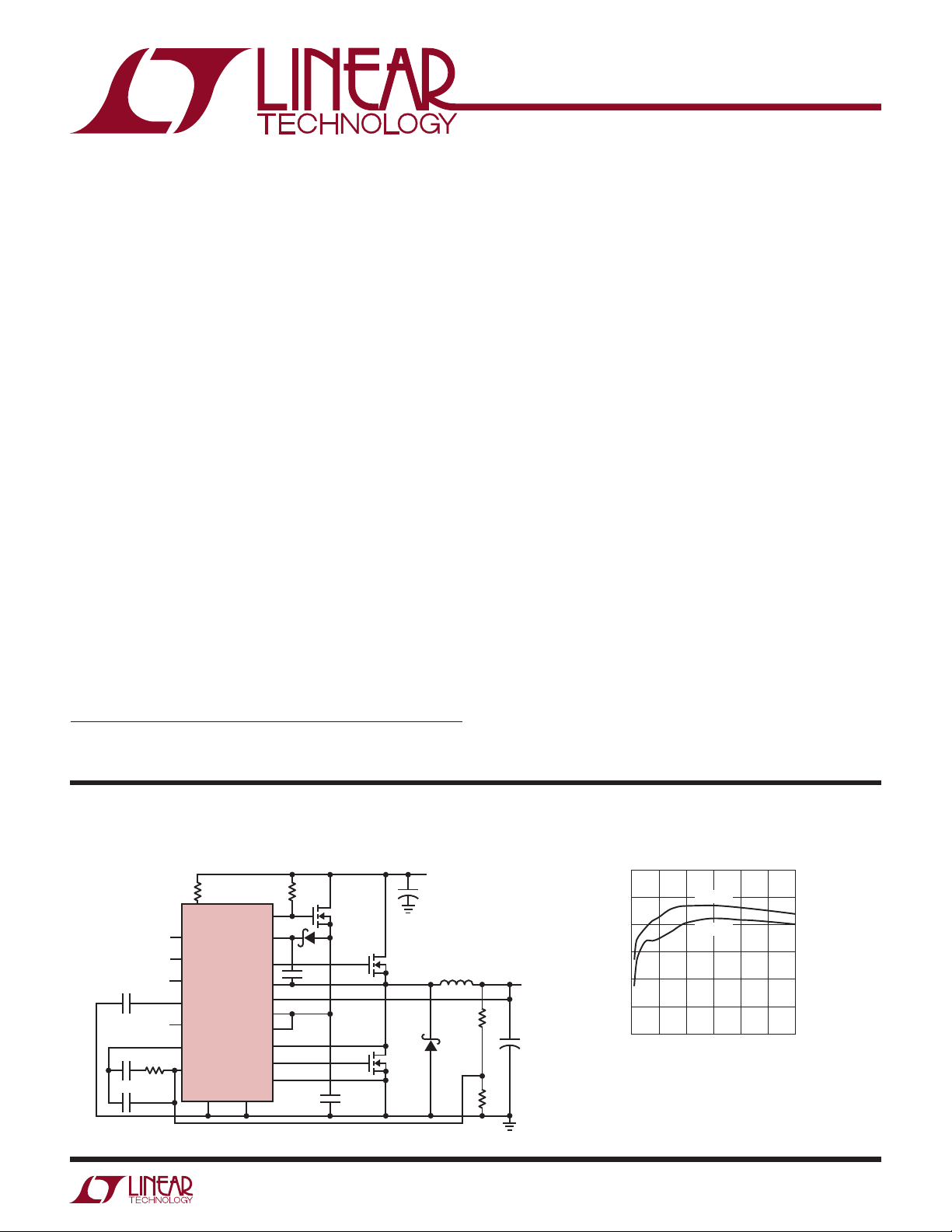
Typical applicaTion
High Efficiency High Voltage Step-Down Converter
274k 100k
I
1000pF
47pF
5pF
200k
ON
PGOOD
V
RNG
MODE/SYNC
SS/TRACK
SHDN
I
TH
V
FB
SGND
LTC3810-5
BGRTN
NDRV
BOOST
EXTV
DRV
INTV
SENSE
SENSE
TG
SW
0.1µF
CC
CC
CC
+
BG
–
ZXMN10A07F
1µF
+
Si7450DP
Si7450DP
V
IN
13V TO 60V
22µF
MBR1100
10µH
14k
1k
Efficiency vs Load Current
100
VIN = 24V
95
V
OUT
12V/6A
+
270µF
38105 TA01
EFFICIENCY (%)
90
85
0
2 3 4
1
LOAD CURRENT (A)
VIN = 42V
5 6
38105 TA01b
38105fd
1
Page 2

LTC3810-5
(Note 1)
Supply Voltages
INTV
(DRV
BOOST (Continuous) .............................. –0.3V to 85V
BOOST (≤400ms) .................................. –0.3V to 95V
BGRTN ........................................................ –5V to 0V
EXTV
(EXTV
(NDRV – INTV
SW, SENSE
SW, SENSE
I
ON
I
ON
SS/TRACK Voltage ....................................... –0.3V to 5V
PGOOD Voltage ............................................ –0.3V to 7V
V
RNG
UVIN Voltages ............................................ –0.3V to 14V
PLL/LPF, FB Voltages ................................ –0.3V to 2.7V
TG, BG, INTV
Operating Junction Temperature Range (Notes 2, 3, 7)
LTC3810E-5 ....................................... –40°C to 125°C
LTC3810I-5 ........................................ –40°C to 125°C
LTC3810H-5 ....................................... –40°C to 150°C
Storage Temperature Range .................. –65°C to 125°C
, DRVCC ...................................... –0.3V to 14V
CC
– BGRTN), (BOOST – SW) ........ –0.3V to 14V
CC
.................................................. –0.3V to 15V
CC
– INTVCC) ..................................–12V to 12V
CC
) Voltage .......................... –0.3V to 10V
CC
+
Voltage (Continuous) .................–1V to 70V
+
Voltage (400ms) ........................–1V to 80V
Voltage (Continuous) ............................ –0.3V to 70V
Voltage (400ms) ................................... –0.3V to 80V
, VON, MODE/SYNC, SHDN,
, EXTVCC RMS Currents ................50mA
CC
pin conFiguraTionabsoluTe MaxiMuM raTings
TOP VIEW
NC
IONNCNCNC
323331 30 29 28 27 26 25
1NC
V
2
ON
V
3
RNG
PGOOD
4
MODE/SYNC
EXPOSED PAD (PIN 33) IS SGND, MUST BE SOLDERED TO PCB
I
V
PLL/LPF
5
6
TH
7
FB
8
9 10 11 12
NC
NC
SS/TRACK
32-LEAD (5mm × 5mm) PLASTIC QFN
UH PACKAGE
= 125°C, θJA = 34°C/W
T
JMAX
BOOSTTGSW
13 14 15 16
UVIN
NDRV
SHDN
SENSE
NC
NC
NC
SENSE
BGRTN
BG
DRV
+
–
CC
24
23
22
21
20
19
18
17
CC
CC
INTV
EXTV
orDer inForMaTion
LEAD FREE FINISH TAPE AND REEL PART MARKING* PACKAGE DESCRIPTION TEMPERATURE RANGE
LTC3810EUH-5#PBF LTC3810EUH-5#TRPBF 38105
LTC3810IUH-5#PBF LTC3810IUH-5#TRPBF 38105
LEAD BASED FINISH TAPE AND REEL PART MARKING PACKAGE DESCRIPTION TEMPERATURE RANGE
LTC3810EUH-5 LTC3810EUH-5#TR 38105
LTC3810IUH-5 LTC3810IUH-5#TR 38105
LTC3810HUH-5 LTC3810HUH-5#TR 38105
Consult LTC Marketing for parts specified with wider operating temperature ranges. *The temperature grade is identified by a label on the shipping container.
For more information on lead free part marking, go to: http://www.linear.com/leadfree/
For more information on tape and reel specifications, go to: http://www.linear.com/tapeandreel/
32-Lead (5mm × 5mm) Plastic QFN
32-Lead (5mm × 5mm) Plastic QFN
32-Lead (5mm × 5mm) Plastic QFN
32-Lead (5mm × 5mm) Plastic QFN
32-Lead (5mm × 5mm) Plastic QFN
–40°C to 125°C
–40°C to 125°C
–40°C to 125°C
–40°C to 125°C
–40°C to 150°C
38105fd
2
Page 3
LTC3810-5
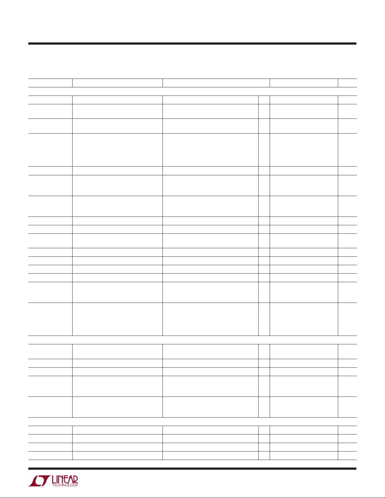
elecTrical characTerisTics
The l denotes specifications which apply over the full operating
temperature range, otherwise specifications are at TA = 25°C (Note 2), INTVCC = DRVCC = V
V
EXTVCC
= V
NDRV
= 5V, V
MODE/SYNC
= V
SENSE
+
= V
SYMBOL PARAMETER CONDITIONS MIN TYP MAX UNITS
Main Control Loop
INTV
CC
I
Q
I
BOOST
V
FB
DV
FB,LINE
V
SENSE(MAX)
V
SENSE(MIN)
I
VFB
(EA) Error Amplifier DC Open Loop Gain 65 100 dB
A
VOL
f
U
INTVCC Supply Voltage
INTVCC Supply Current
Shutdown Current
INTV
CC
BOOST Supply Current SHDN > 1.5V (Note 5)
Feedback Voltage (Note 4)
Feedback Voltage Line Regulation 5V < INTVCC < 14V (Note 4)
Maximum Current Sense Threshold V
Minimum Current Sense Threshold V
Feedback Current VFB = 0.8V 20 150 nA
Error Amp Unity-Gain Crossover
Frequency
V
MODE/SYNC
I
MODE/SYNC
V
SHDN
I
SHDN
V
UVIN
V
VCCUV
MODE/SYNC Threshold V
MODE/SYNC Current MODE/SYNC = 5V 0 1 µA
Shutdown Threshold 1.2 1.5 2 V
SHDN Pin Input Current 0 1 µA
UVIN Undervoltage Lockout UVIN Rising
INTVCC Undervoltage Lockout
Linear Regulator Mode
External Supply Mode
Trickle-Charge Mode
Oscillator and Phase-Locked Loop
t
ON
t
ON(MIN)
t
OFF(MIN)
t
ON(PLL)
On-Time ION = 100µA
Minimum On-Time ION = 2000µA 100 ns
Minimum Off-Time 250 350 ns
tON Modulation Range by PLL
Down Modulation
Up Modulation
I
PLL/LPF
Phase Detector Output Current
Sinking Capability
Sourcing Capability
Driver
I
BG,PEAK
R
BG,SINK
I
TG,PEAK
R
TG,SINK
BG Driver Peak Source Current VBG = 0V 0.7 1 A
BG Driver Pull-Down R
DS(ON)
TG Driver Peak Source Current VTG – VSW = 0 0.7 1 A
TG Driver Pull-Down R
DS(ON)
SENSE
–
= V
= VSW = 0V, unless otherwise specified.
BGRTN
SHDN > 1.5V (Notes 4, 5)
SHDN = 0V
SHDN = 0V
0°C to 85°C
–40°C to 85°C
–40°C to 125°C (I-Grade)
–40°C to 150°C (H-Grade)
= 2V, VFB = 0.76V
RNG
= 0V, VFB = 0.76V
V
RNG
= INTVCC, VFB = 0.76V
V
RNG
= 2V, VFB = 0.84V
RNG
= 0V, VFB = 0.84V
V
RNG
= INTVCC, VFB = 0.84V
V
RNG
(Note 6) 25 MHz
MODE/SYNC
Rising 0.75 0.8 0.85 V
UVIN Falling
Hysteresis
Rising, I
INTV
CC
Rising, NDRV = INTV
INTV
CC
Rising, NDRV = INTVCC, EXTV
INTV
CC
Falling
INTV
CC
= 300µA
I
ON
ION = 100µA, V
ION = 100µA, V
f
< fSW
PLLIN
> f
f
PLLIN
SW
NDRV
PLL/LPF
PLL/LPF
= 100µA
= 0.6V
= 1.8V
= EXTVCC
CC
CC
BOOST
= 0
= VON = V
l
4.35 14 V
= SHDN = UVIN =
RNG
3
240
600
270 0400
l
l
l
l
l
0.796
0.794
0.792
0.792
0.792
256
70
170
0.800
0.800
0.800
0.800
0.800
0.804
0.806
0.806
0.808
0.812
0.002 0.02 %/V
320
95
215
384
120
260
–300
–85
–200
l
l
l
l
l
0.86
0.78
0.07
4.05
4.05
8.70
0.89
0.80
0.10
4.2
4.2
9
0.92
0.82
0.12
4.35
4.35
9.30
3.7
1.55
515
2.2
0.6
1.85
605
2.15
695
3.6
1.2
15
–25
1 1.5 Ω
1 1.5 Ω
6
5
5
1.8
mA
µA
µA
µA
mV
mV
mV
mV
mV
mV
µA
µA
38105fd
V
V
V
V
V
V
V
V
V
V
V
V
µs
ns
µs
µs
3
Page 4

LTC3810-5
elecTrical characTerisTics
The l denotes specifications which apply over the full operating
temperature range, otherwise specifications are at TA = 25°C (Note 2), INTVCC = DRVCC = V
V
EXTVCC
= V
NDRV
= 5V, V
MODE/SYNC
= V
SENSE
+
= V
SYMBOL PARAMETER CONDITIONS MIN TYP MAX UNITS
PGOOD Output
DV
FBOV
DV
FB,HYST
V
PGOOD
I
PGOOD
PGOOD Upper Threshold
PGOOD Lower Threshold
PGOOD Hysterisis VFB Returning 1.5 3 %
PGOOD Low Voltage I
PGOOD Leakage Current V
PG Delay PGOOD Delay V
Tracking
I
SS/TRACK
V
FB,TRACK
Regulators
V
CC
V
EXTVCC
V
INTVCC,1
DV
EXTVCC,1
DV
LOADREG,1
V
INTVCC,2
DV
LOADREG,2
I
NDRV
I
NDRVTO
SS/TRACK Source Current V
Feedback Voltage at Tracking V
EXTVCC Switchover Voltage
Rising
EXTV
CC
Hysterisis
EXTV
CC
INTVCC Voltage from EXTV
V
EXTVCC
- V
at Dropout ICC = 20mA, V
INTVCC
CC
INTVCC Load Regulation from EXTV
INTVCC Voltage from NDRV Regulator Linear Regulator in Operation 5.2 5.5 5.8 V
INTVCC Load Regulation from NDRV ICC = 0mA to 20mA, V
Current into NDRV Pin V
Linear Regulator Timeout Enable
Threshold
V
CCSR
I
CCSR
Maximum Supply Voltage Trickle Charger Shunt Regulator 15 V
Maximum Current into NDRV/INTV
SENSE
CCICC
CC
–
= V
= VSW = 0V, unless otherwise specified.
BGRTN
VFB Rising
Falling
V
FB
= 5mA 0.3 0.6 V
PGOOD
= 5V 0 2 µA
PGOOD
Falling 120 µs
FB
> 0.5V 0.7 1.4 2.5 µA
SS/TRACK
= 0V, ITH = 1.2V (Note 4)
TRACK
= 0.5V, ITH = 1.2V (Note 4)
V
TRACK
6V < V
= 0mA to 20mA, V
NDRV
< 15V 5.2 5.5 5.8 V
EXTVCC
= 5V 75 150 mV
EXTVCC
= 10V 0.01 %
EXTVCC
= 0 0.01 %
EXTVCC
– V
= 3V 20 40 60 µA
INTVCC
Trickle Charger Shunt Regulator,
≤ 16.7V (Note 8)
INTV
CC
BOOST
= VON = V
–7.5
0.48
l
4.45
= SHDN = UVIN =
RNG
7.5
–0.018
0.1
10
–10
0.5
4.7
0.25
12.5
–12.5
0.52
210 270 350 µA
10 mA
%
%
0.4
V
V
V
V
Note 1: Stresses beyond those listed under Absolute Maximum Ratings
may cause permanent damage to the device. Exposure to any Absolute
Maximum Rating condition for extended periods may affect device
reliability and lifetime.
Note 2: The LTC3810-5 is tested under pulsed load conditions such that
≈ TA. The LTC3810E-5 is guaranteed to meet performance specifications
T
J
from 0°C to 85°C. Specifications over the –40°C to 125°C operating
junction temperature range are assured by design, characterization and
correlation with statistical process controls. The LTC3810I-5 is guaranteed
to meet performance specifications over the full –40°C to 125°C operating
junction temperature range. The LTC3810H-5 is guaranteed to meet
performance specifications over the full –40°C to 150°C operating junction
temperature range. High junction temperatures degrade operating lifetimes;
operating lifetime is derated for junction temperatures greater than 125°C.
Note 3: T
is calculated from the ambient temperature TA and power
J
Similar Parts Comparison
PARAMETER LTC3810 LTC3810-5 LTC3812-5
Maximum V
IN
100V 60V 60V
MOSFET Gate Drive 6.35V to 14V 4.5V to 14V 4.5V to 14V
CC
CC
UV
UV
+
–
6.2V 4.2V 4.2V
6V 4V 4V
INTV
INTV
4
dissipation PD according to the following formula:
LTC3810-5: T
Note 4: The LTC3810-5 is tested in a feedback loop that servos V
reference voltage with the I
= TA + (PD • 34°C/W)
J
pin forced to a voltage between 1V and 2V.
TH
to the
FB
Note 5: The dynamic input supply current is higher due to the power
MOSFET gate charging being delivered at the switching frequency
• f
(Q
).
G
OSC
Note 6: Guaranteed by design. Not subject to test.
Note 7: This IC includes overtemperature protection that is intended
to protect the device during momentary overload conditions. Junction
temperature will exceed 150°C when overtemperature protection is active.
Continuous operation above the specified maximum operating junction
temperature may impair device reliability.
Note 8: I
is the sum of current into NDRV and INTVCC.
CC
38105fd
Page 5

LTC3810-5
Typical perForMance characTerisTics
Load Transient Response
V
OUT
100mV/DIV
I
OUT
5A/DIV
VIN = 48V
0A TO 5A LOADSTEP
FRONT PAGE CIRCUIT
Short-Circuit/
Foldback Operation
V
OUT
5V/DIV
V
FB
0.5V/DIV
I
L
5A/DIV
VIN = 48V
FRONT PAGE CIRCUIT
50µs/DIV
200µs/DIV
38105 G01
38105 G04
INTV
5V/DIV
V
OUT
5V/DIV
V
50V/DIV
5A/DIV
V
OUT
5V/DIV
SS/TRACK
0.5V/DIV
V
0.5V/DIV
5A/DIV
CC
IN
I
L
FB
I
L
Start-Up
VIN = 48V
= 1A
I
LOAD
MODE/SYNC = 0V
FRONT PAGE CIRCUIT
Tracking
V
= 48V
IN
= 1A
I
LOAD
MODE/SYNC = 0V
FRONT PAGE CIRCUIT
INTV
500µs/DIV
500µs/DIV
CC
38105 G02
SS/TRACK
V
FB
38105 G05
V
OUT
10V/DIV
SS/TRACK
4V/DIV
5A/DIV
V
OUT
100mV/DIV
I
0.5V/DIV
2A/DIV
Short-Circuit/
Fault Timeout Operation
I
L
VIN = 48V
= 0.1Ω
R
SHORT
FRONT PAGE CIRCUIT
10ms/DIV
Pulse Skip Mode Operation
TH
I
L
VIN = 48V
= 100mA
I
OUT
MODE/SYNC = INTV
FRONT PAGE CIRCUIT
20µs/DIV
CC
38105 G03
38105 G06
Efficiency vs Input Voltage
100
I
OUT
90
EFFICIENCY (%)
80
V
= 12V
OUT
Si7852 MOSFETs
f = 250kHz
70
10 20
I
OUT
40
30
INPUT VOLTAGE (V)
= 5A
= 0.5A
Efficiency vs Load Current
100
95
VIN = 12V
90
85
EFFICIENCY (%)
80
75
70
0
50
60
70
80
38105 G07
1
VIN = 36V
V
= 5V
OUT
Si7850 MOSFETs
MODE/SYNC = INTV
f = 250kHz
2 3 4
LOAD CURRENT (A)
VIN = 60V
CC
5 76
38105 G08
Frequency vs Input Voltage
280
270
I
260
250
FREQUENCY (kHz)
240
MODE/SYNC = 0V
FRONT PAGE CIRCUIT
230
10 20
OUT
I
OUT
30
40
INPUT VOLTAGE (V)
= 0A
= 5A
50
60
70
80
38105 G09
38105fd
5
Page 6
LTC3810-5
680
230
REFERENCE VOLTAGE (V)
0.803
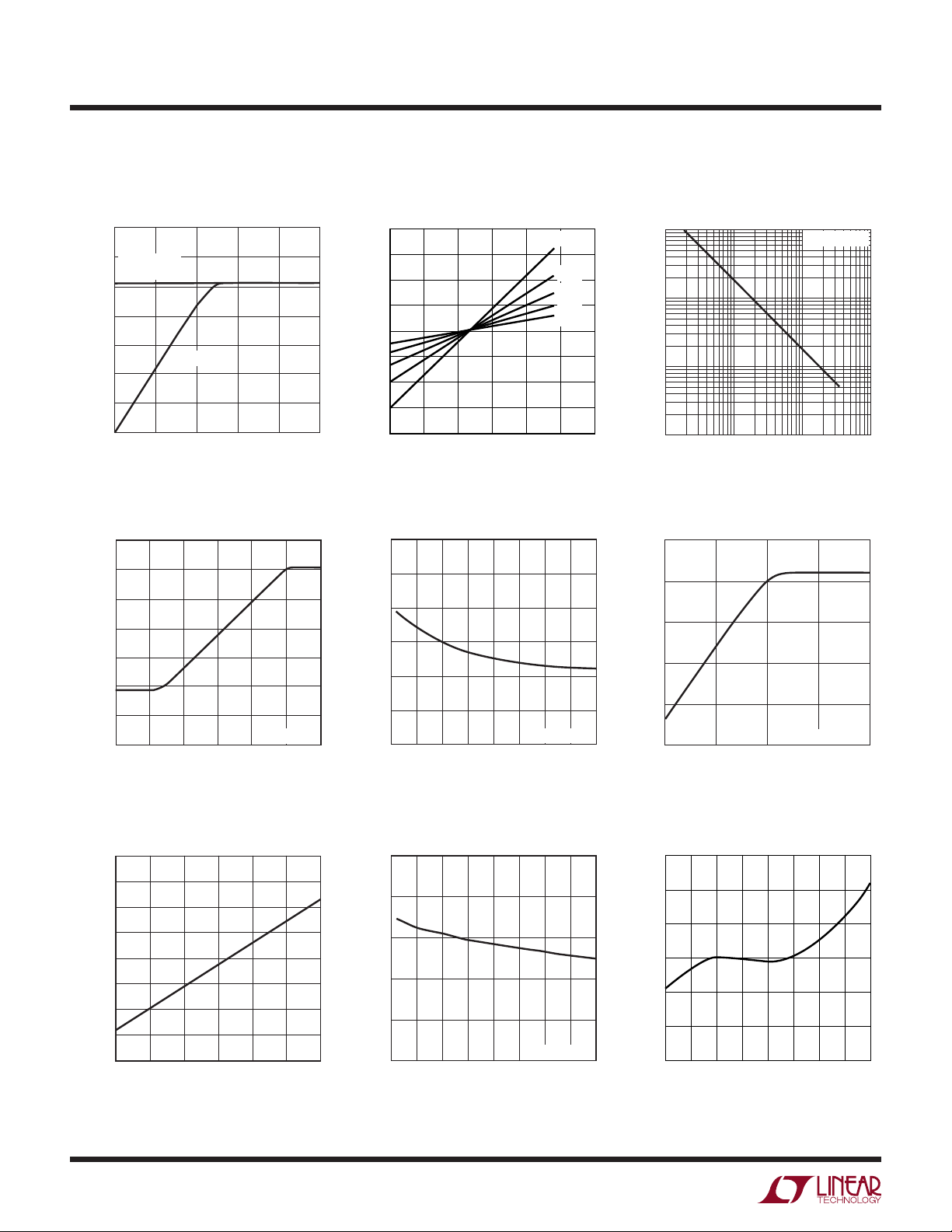
Typical perForMance characTerisTics
Frequency vs Load Current
350
300
FORCED
CONTINUOUS
250
200
150
FREQUENCY (kHz)
100
50
0
0
PULSE SKIP
1 2 3 5
LOAD CURRENT (A)
On-Time vs V
700
600
500
400
300
ON-TIME (ns)
200
100
0
0
0.5 1
ON
VON VOLTAGE (V)
Voltage
ION = 300µA
2 3
1.5 2.5
4
38105 G10
38105 G13
Current Sense Threshold
vs ITH Voltage
400
300
200
100
0
–100
–200
CURRENT SENSE THRESHOLD (mV)
–300
–400
0.5 1.0 2.0
0
ITH VOLTAGE (V)
1.5
On-Time vs Temperature
660
640
620
ON-TIME (ns)
600
580
560
–50
–25 0 50 100 150125
25 75
TEMPERATURE (°C)
ION = 300µA
On-Time vs ION Current
3.0
10000
1000
ON-TIME (ns)
100
10
10
100 1000 10000
ION CURRENT (µA)
V
= 2V
RNG
1.4V
1V
0.7V
0.5V
2.5
38105 G11
VON = INTV
CC
38105 G12
Current Limit Foldback
250
200
150
100
50
V
= INTV
38105 G14
MAXIMUM CURRENT SENSE THRESHOLD (mV)
0
0.2
0
0.4
VFB (V)
RNG
0.6
CC
0.8
38105 G15
400
300
200
100
MAXIMUM CURRENT SENSE THRESHOLD (mV)
0
0.5
6
Maximum Current Sense
Threshold vs V
V
Voltage
RNG
1 1.5
VOLTAGE (V)
RNG
38105 G16
Maximum Current Sense
Threshold vs Temperature
220
210
200
190
MAXIMUM CURRENT SENSE THRESHOLD (mV)
180
2
–50 25 75–25 0 50 100 150125
TEMPERATURE (°C)
Reference Voltage vs
Temperature
0.802
0.801
0.800
0.799
0.798
V
= INTV
RNG
38105 G17
CC
0.797
–50 25 75–25 0 50 100 150125
TEMPERATURE (°C)
38105 G18
38105fd
Page 7
LTC3810-5
PEAK SOURCE CURRENT (A)
1.5
7
RESISTANCE (Ω)
5
400
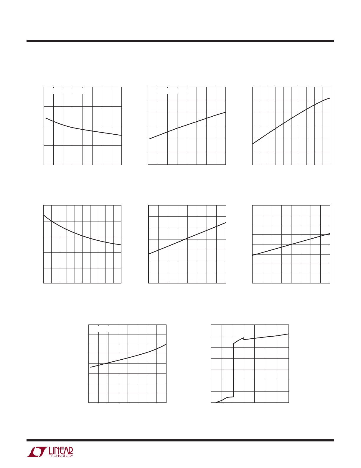
Typical perForMance characTerisTics
Driver Peak Source Current
vs Temperature
V
= V
BOOST
1.0
0.5
–50 25 75–25 0 50 100 150125
Driver Pull-Down R
= 5V
INTVCC
TEMPERATURE (°C)
DS(ON)
vs Supply Voltage
1.1
1.0
0.9
(Ω)
DS(ON)
0.8
R
0.7
38105 G19
Driver Pull-Down R
DS(ON)
vs Temperature
1.75
V
= V
BOOST
1.50
1.25
(Ω)
1.00
DS(ON)
R
0.75
0.50
0.25
–50 25 75–25 0 50 100 150125
= 5V
INTVCC
TEMPERATURE (°C)
EXTVCC LDO Resistance at
Dropout vs Temperature
6
5
4
3
2
1
38105 G20
Driver Peak Source Current
vs Supply Voltage
3.0
2.5
2.0
1.5
1.0
PEAK SOURCE CURRENT (A)
0.5
0
4 5 7 9 11 13
6 8 10 12
DRVCC/BOOST VOLTAGE (V)
INTVCC Current vs Temperature
4
3
CURRENT (mA)
CC
INTV
2
14
38105 G21
0.6
4
6
5 7
DRVCC/BOOST VOLTAGE (V)
9 1413
8
300
200
CURRENT (µA)
CC
INTV
100
0
11
12
10
38105 G22
Shutdown Current
INTV
CC
–50 25 75–25 0 50 100 150125
vs Temperature
INTVCC = 5V
0
–50 25 75–25 0 50 100 150125
TEMPERATURE (°C)
38105 G25
TEMPERATURE (°C)
1
–50 25 75–25 0 50 100 150125
38105 G23
INTVCC Current vs INTVCC Voltage
3.5
3.0
2.5
2.0
1.5
CURRENT (mA)
CC
1.0
INTV
0.5
0
0
2 4
INTVCC VOLTAGE (V)
8 12 14
6 10
TEMPERATURE (°C)
38105 G26
38105fd
7
Page 8

LTC3810-5
SS/TRACK CURRENT (µA)
SHUTDOWN THRESHOLD (V)
2.2
Typical perForMance characTerisTics
INTVCC Shutdown Current
vs INTVCC Voltage
300
250
200
150
CURRENT (µA)
CC
100
INTV
50
0
0
I
TH
2 4
Voltage
6 10
INTVCC VOLTAGE (V)
vs Load Current
3.0
2.5
2.0
1.5
VOLTAGE (V)
TH
I
1.0
0.5
0
0
1 2
3 5
LOAD CURRENT (A)
8 12 14
38105 G27
V
= 1V
RNG
FRONT PAGE CIRCUIT
4 6 7
38105 G29
SS/TRACK Pull-Up Current
vs Temperature
3
2
1
0
–50 25 75–25 0 50 100 150125
Shutdown Threshold
vs Temperature
2.0
1.8
1.6
1.4
1.2
1.0
0.8
0.6
–50 25 75–25 0 50 100 150125
TEMPERATURE (°C)
TEMPERATURE (°C)
38105 G28
38105 G30
8
38105fd
Page 9

pin FuncTions
LTC3810-5
VON (Pin 2): On-Time Voltage Input. Voltage trip point
for the on-time comparator. Tying this pin to the output
voltage or to an external resistive divider from the output
makes the on-time proportional to V
. The comparator
OUT
defaults to 0.7V when the pin is grounded and defaults to
2.4V when the pin is connected to INTV
INTV
V
in high V
CC
(Pin 3): Sense Voltage Limit Set. The voltage at this
RNG
applications to use a lower RON value.
OUT
. Tie this pin to
CC
pin sets the nominal sense voltage at maximum output
current and can be set from 0.5V to 2V by a resistive divider from INTV
. The nominal sense voltage defaults to
CC
95mV when this pin is tied to ground, and 215mV when
tied to INTV
CC
.
PGOOD (Pin 4): Power Good Output. Open-drain logic
output that is pulled to ground when the output voltage
is not between ±10% of the regulation point. The output
voltage must be out of regulation for at least 120µs before
the power good output is pulled to ground.
MODE/SYNC (Pin 5): Pulse Skip Mode Enable/Sync Pin.
This multifunction pin provides pulse skip mode enable/
disable control and an external clock input to the phase
detector. Pulling this pin below 0.8V or to an external
logic-level synchronization signal disables pulse skip mode
operation and forces continuous operation. Pulling this
pin above 0.8V enables pulse skip mode operation. For a
clock input, the phase-locked loop will force the rising top
gate signal to be synchronized with the rising edge of the
clock signal.This pin can also be connected to a feedback
resistor divider from a secondary winding on the inductor
to regulate a second output voltage.
(Pin 6): Error Amplifier Compensation Point and Cur-
I
TH
rent Control Threshold. The current comparator threshold
increases with this control voltage. The voltage ranges
from 0V to 2.6V with 1.2V corresponding to zero sense
voltage (zero current).
(Pin 7): Feedback Input. Connect VFB through a resistor
V
FB
divider network to V
to set the output voltage.
OUT
PLL/LPF (Pin 8): The phase-locked loop’s lowpass filter
is tied to this pin. The voltage at this pin defaults to 1.2V
when the IC is not synchronized with an external clock at
the MODE/SYNC pin.
SS/TRACK (Pin 9): Soft-Start/Tracking Input. For soft-start,
a capacitor to ground at this pin sets the ramp rate of the
output voltage (approximately 0.6s/µF). For coincident or
ratiometric tracking, connect this pin to a resistive divider
between the voltage to be tracked and ground.
SHDN (Pin 12): Shutdown Pin. Pulling this pin below
1.5V will shut down the LTC3810-5, turn off both of the
external MOSFET switches and reduce the quiescent supply current to 240µA.
UVIN (Pin 13): UVLO Input. This pin is input to the internal
UVLO and is compared to an internal 0.8V reference. An
external resistor divider is connected to this pin and the
input supply to program the undervoltage lockout voltage.
When UVIN is less than 0.8V, the LTC3810-5 is shut down.
NDRV (Pin 14): Drive Output for External Pass Device of
the Linear Regulator for INTV
. Connect to the gate of
CC
an external NMOS pass device and a pull-up resistor to
the input voltage V
EXTV
(Pin 15): External Driver Supply Voltage. When
CC
IN
.
this voltage exceeds 4.7V, an internal switch connects this
pin to INTV
through an LDO and turns off the exter nal
CC
MOSFET connected to NDRV, so that controller and gate
drive are drawn from EXTV
INTV
(Pin 16): Main Supply Pin. All internal circuits ex-
CC
cept the output drivers are powered from this pin. INTV
CC
.
CC
should be bypassed to ground (Pin 10) with at least a 0.1µF
capacitor in close proximity to the LTC3810-5.
(Pin 17): Driver Supply Pin. DRVCC supplies power
DRV
CC
to the BG output driver. This pin is normally connected to
INTV
. DRVCC should be bypassed to BGRTN (Pin 20)
CC
with a low ESR (X5R or better) 1µF-10µF capacitor in close
proximity to the LTC3810-5.
38105fd
9
Page 10

LTC3810-5
pin FuncTions
BG (Pin 18): Bottom Gate Drive. The BG pin drives the
gate of the bottom N-channel synchronous switch MOSFET.
This pin swings from BGRTN to DRV
BGRTN (Pin 19): Bottom Gate Return. This pin connects to
the source of the pulldown MOSFET in the BG driver and
is normally connected to ground. Connecting a negative
supply to this pin allows the synchronous MOSFET ’s gate
to be pulled below ground to help prevent false turn-on
during high dV/dt transitions on the SW node. See the
Applications Information section for more details.
+
SENSE
parator Input. The (+) input to the current comparator is
normally connected to SW unless using a sense resistor.
The (–) input is used to accurately kelvin sense the bottom
side of the sense resistor or MOSFET.
SW (Pin 25): Switch Node Connection to Inductor and
Bootstrap Capacitor. The voltage swing at this pin is –0.7V
(a Schottky diode (external) voltage drop) to V
, SENSE– (Pin 24, Pin 20): Current Sense Com-
CC
.
.
IN
TG (Pin 26): Top Gate Drive. The TG pin drives the gate of
the top N-channel synchronous switch MOSFET. The TG
driver draws power from the BOOST pin and returns to the
SW pin, providing true floating drive to the top MOSFET.
BOOST (Pin 27): Top Gate Driver Supply. The BOOST pin
supplies power to the floating TG driver. BOOST should
be bypassed to SW with a low ESR (X5R or better) 0.1µF
capacitor. An additional fast recovery Schottky diode from
to the BOOST pin will create a complete floating
DRV
CC
charge-pumped supply at BOOST.
(Pin 31): On-Time Current Input. Tie a resistor from VIN
I
ON
to this pin to set the one-shot timer current and thereby
set the switching frequency.
SGND (Exposed Pad Pin 33): Signal Ground. All smallsignal components should connect to this ground and
eventually connect to PGND at one point.
10
38105fd
Page 11
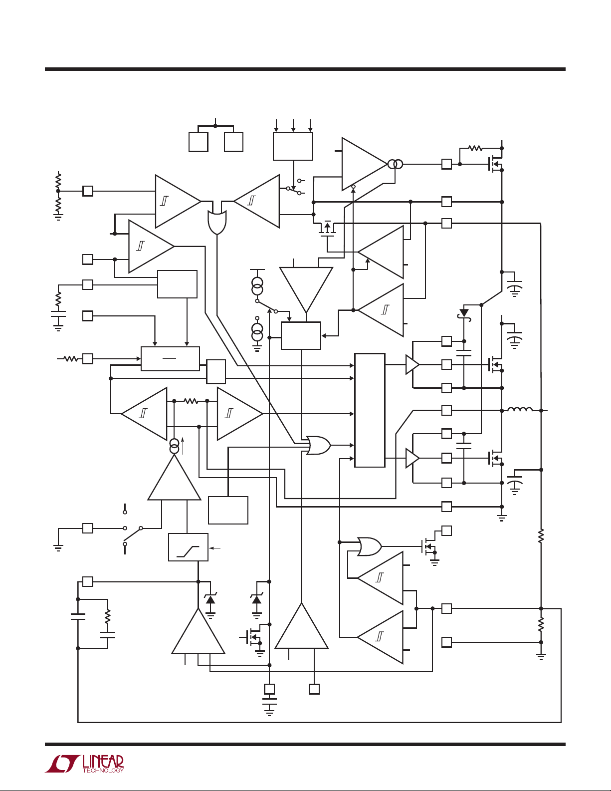
FuncTional DiagraM
LTC3810-5
V
V
IN
IN
R
UV1
R
UV2
R
ON
UVIN
13
0.8V
MODE/SYNC
5
PLL/LPF
8
V
ON
2
I
ON
31
V
RNG
3
I
TH
6
C
C2
INTV
CC
5V
REG
0.8V
REF
–
V
UV
IN
+
EXTV
INTV
CC
UV
+
F
–
PLL-SYNC
1.4µA
CC
+
–
N
DRV
INTV
MODE
LOGIC
270µA
–
CC
9V
4.2V
INTV
CC
V
IN
5.5V
+
NDRV
14
M3
–
OFF
INTV
EXTV
CC
16
CC
15
+
5.5V
+
ON
–
+
+
V
D
BOOST
27
TG
26
SW
25
SENSE
24
DRV
17
BG
18
BGRTN
19
SENSE
20
PGOOD
4
V
7
SGND
12
B
+
CC
–
FB
4.7V
–
V
VON
tON = (76pF)
I
ION
20k
+
I
CMP
–
R
S Q
100nA
+
I
REV
TIMEOUT
LOGIC
DRV OFF
FCNT
ON
SWITCH
LOGIC
–
SHDN
OV
×
1.4V
FOLDBACK
0.7V
R
C
C
C1
0.8V
OVERTEMP
SENSE
ITH’
FB
0.72V
+
UV
2.6V 4V
1.5V
SS/TRACK
9
+
RUN
SHDN
–
SHDN
12
EA
FAULT
–
+
+
–
+
OV
0.88V
–
IN
+
C
IN
C
B
M1
L1
C
VCC
M2
V
OUT
+
C
OUT
R
FB1
R
FB2
38105 FD
38105fd
11
Page 12
LTC3810-5
operaTion
Main Control Loop
The LTC3810-5 is a current mode controller for DC/
DC step-down converters. In normal operation, the top
MOSFET is turned on for a fixed interval determined by
a one-shot timer (OST). When the top MOSFET is turned
off, the bottom MOSFET is turned on until the current
comparator I
trips, restarting the one-shot timer and
CMP
initiating the next cycle. Inductor current is determined
–
by sensing the voltage between the SENSE
and SENSE+
pins using a sense resistor or the bottom MOSFET onresistance. The voltage on the I
pin sets the comparator
TH
threshold corresponding to the inductor valley current.
The fast 25MHz error amplifier EA adjusts this voltage by
comparing the feedback signal V
to the internal 0.8V
FB
reference voltage. If the load current increases, it causes a
drop in the feedback voltage relative to the reference. The
voltage then rises until the average inductor current
I
TH
again matches the load current.
The operating frequency is determined implicitly by the top
MOSFET on-time and the duty cycle required to maintain
regulation. The one-shot timer generates an on time that is
proportional to the ideal duty cycle, thus holding frequency
approximately constant with changes in V
frequency can be adjusted with an external resistor R
. The nominal
IN
ON
.
For applications with stringent constant frequency requirements, the LTC3810-5 can be synchronized with an
external clock. By programming the nominal frequency
the same as the external clock frequency, the LTC3810-5
behaves as a constant frequency part against the load and
supply variations.
Pulling the SHDN pin low forces the controller into its
shutdown state, turning off both M1 and M2. Forcing a
voltage above 1.5V will turn on the device.
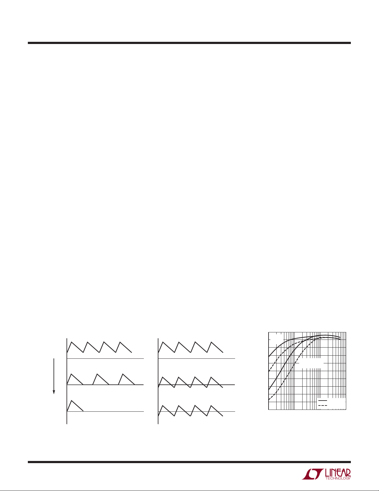
Pulse Skip Mode
The LTC3810-5 can operate in one of two modes selectable
with the MODE/SYNC pin—pulse skip mode or forced continuous mode (see Figure 1). Pulse skip mode is selected
when increased efficiency at light loads is desired (see
Figure 2). In this mode, the bottom MOSFET is turned off
when inductor current reverses to minimize efficiency loss
due to reverse current flow and gate charge switching.
At low load currents, I
will drop below the zero current
TH
level (1.2V) shutting off both switches. Both switches will
remain off with the output capacitor supplying the load
current until the I
voltage rises above the zero current
TH
level to initiate another cycle. In this mode, frequency is
proportional to load current at light loads.
Pulse skip mode operation is disabled by comparator F
when the MODE/SYNC pin is brought below 0.8V, forcing
continuous synchronous operation. Forced continuous
mode is less efficient due to resistive losses, but has the
advantage of better transient response at low currents,
approximately constant frequency operation, and the ability
to maintain regulation when sinking current.
PULSE SKIP MODE
0A
DECREASING
LOAD
CURRENT
0A
0A
Figure 1. Comparison of Inductor Current Waveforms for Pulse Skip Mode
and Forced Continuous Operation
FORCED CONTINUOUS
0A
0A
0A
12
38105 F01
100
PULSE
90
SKIP
80
70
60
50
40
EFFICIENCY (%)
30
20
10
0
0.01
Figure 2. Efficiency in Pulse Skip/
Forced Continuous Modes
FORCED
CONTINUOUS
0.1 1 10
LOAD (A)
VIN = 12V
= 42V
V
IN
38105 F02
38105fd
Page 13
operaTion
LTC3810-5
Fault Monitoring/Protection
Constant on-time current mode architecture provides accurate cycle-by-cycle current limit protection—a feature
that is very important for protecting the high voltage power
supply from output short circuits. The cycle-by-cycle current monitor guarantees that the inductor current will never
exceed the value programmed on the V
RNG
pin.
Foldback current limiting provides further protection if the
output is shorted to ground. As V
current threshold voltage I
is pulled down and clamped
THB
drops, the buffered
FB
to 1V. This reduces the inductor valley current level to
one-sixth of its maximum value as V
approaches 0V.
FB
Foldback current limiting is disabled at start-up.
Overvoltage and undervoltage comparators OV and UV
pull the PGOOD output low if the output feedback voltage
exits a ±10% window around the regulation point after the
internal 120µs power bad mask timer expires. Furthermore,
in an overvoltage condition, M1 is turned off and M2 is
turned on immediately and held on until the overvoltage
condition clears.
skip mode operation, where it is possible that the bottom
MOSFET will be off for an extended period of time, an
internal timeout guarantees that the bottom MOSFET is
turned on at least once every 25µs for one on-time period
to refresh the bootstrap capacitor.
The bottom driver has an additional feature that helps
minimize the possibility of external MOSFET shoot-through.
When the top MOSFET turns on, the switch node dV/dt
pulls up the bottom MOSFET’s internal gate through the
Miller capacitance, even when the bottom driver is holding
the gate terminal at ground. If the gate is pulled up high
enough, shoot-through between the top side and bottom
side MOSFETs can occur. To prevent this from occurring,
the bottom driver return is brought out as a separate pin
(BGRTN) so that a negative supply can be used to reduce
the effect of the Miller pull-up. For example, if a –2V supply is used on BGRTN, the switch node dV/dt could pull
the gate up 2V before the V
of the bottom MOSFET has
GS
more than 0V across it.
DRV
CC
V
IN
The LTC3810-5 provides two undervoltage lockout comparators—one for the INTV
the input supply V
. The INTVCC UV threshold is 4.2V to
IN
/DRVCC supply and one for
CC
guarantee that the MOSFETs have sufficient gate drive
voltage before turning on. The V
UV threshold (UVIN pin)
IN
is 0.8V with 10% hysteresis which allows programming
the V
connected to V
threshold with the appropriate resistor divider
IN
. If either comparator inputs are under
IN
the UV threshold, the LTC3810-5 is shut down and the
drivers are turned off.
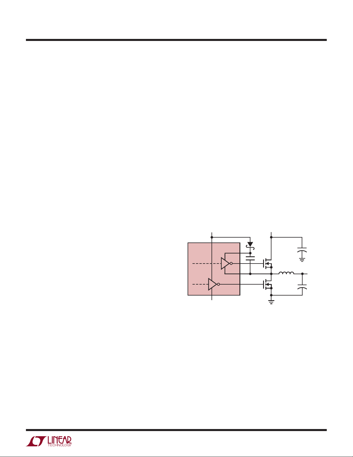
Strong Gate Drivers
The LTC3810-5 contains very low impedance drivers capable of supplying amps of current to slew large MOSFET
gates quickly. This minimizes transition losses and allows
paralleling MOSFETs for higher current applications. A
60V floating high side driver drives the top side MOSFET
and a low side driver drives the bottom side MOSFET
(see Figure 3). The bottom side driver is supplied directly
from the DRV
from floating bootstrap capacitor, C
pin. The top MOSFET drivers are biased
CC
, which normally is
B
recharged during each off cycle through an external diode
from DRV
when the top MOSFET turns off. In pulse
CC
D
LTC3810-5
Figure 3. Floating TG Driver Supply and Negative BG Return
DRV
BGRTN
0V TO –5V
CC
BOOST
TG
SW
BG
B
C
B
M1
M2
+
C
IN
L
38105 F03
V
OUT
+
C
OUT
IC/Driver Supply Power
The LTC3810-5’s internal control circuitry and top and
bottom MOSFET drivers operate from a supply voltage
(INTV
, DRVCC pins) in the range of 4.5V to 14V. The
CC
LTC3810-5 has two integrated linear regulator controllers
to easily generate this IC/driver supply from either the high
voltage input or from the output voltage. For best efficiency
the supply is derived from the input voltage during start-up
and then derived from the lower voltage output as soon
as the output is higher than 4.7V. Alternatively, the supply
can be derived from the input continuously if the output is
38105fd
13
Page 14
LTC3810-5
operaTion
<4.7V or an external supply in the appropriate range can
be used. The LTC3810-5 will automatically detect which
mode is being used and operate properly.
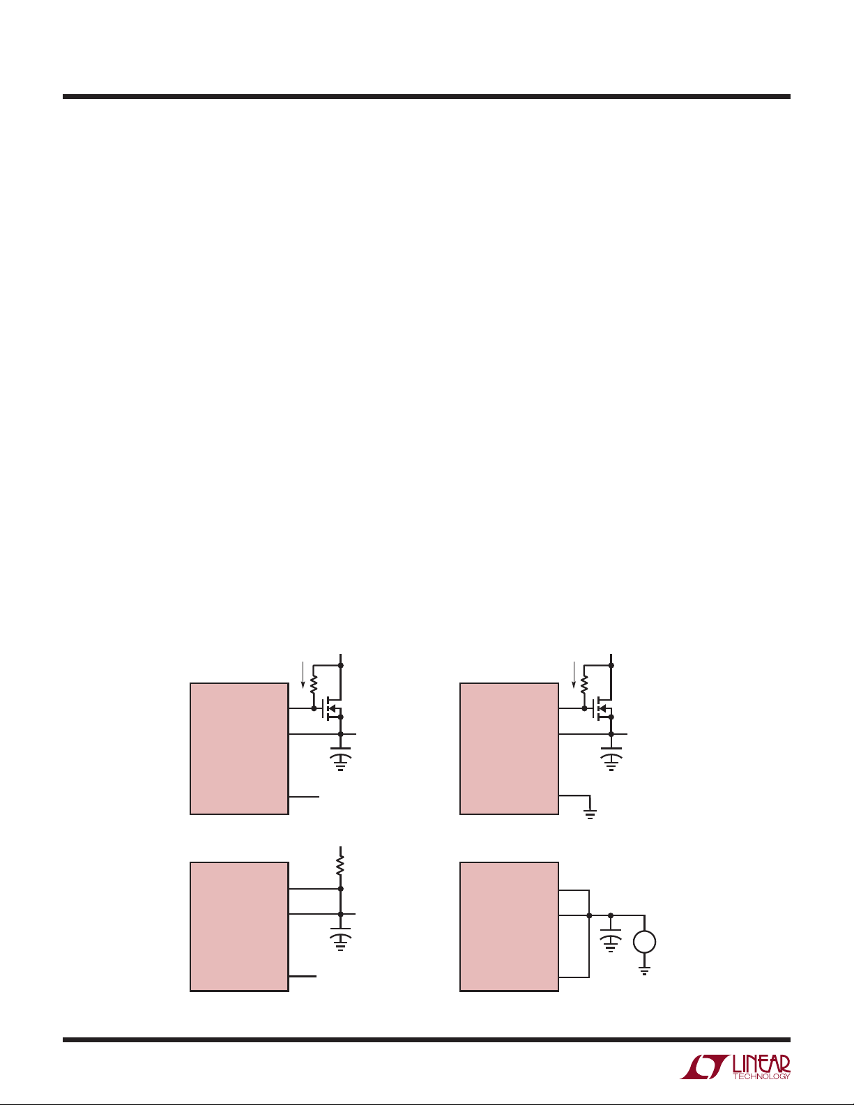
The four possible operating modes for generating this
supply are summarized as follows (see Figure 4):
1. LTC3810-5 generates a 5.5V start-up supply from a small
external SOT23 N-channel MOSFET acting as linear
regulator with drain connected to V
and gate controlled
IN
by the LTC3810-5’s internal linear regulator controller
through the NDRV pin. As soon as the output voltage
reaches 4.7V, the 5.5V IC/driver supply is derived from
the output through an internal low-dropout regulator to
optimize efficiency. If the output is lost due to a short,
the LTC3810-5 goes through repeated low duty cycle
soft-start cycles (with the drivers shut off in between)
to attempt to bring up the output without burning up
the SOT23 MOSFET. This scheme eliminates the long
start-up times associated with a conventional trickle
charger by using an external MOSFET to quickly charge
the IC/driver supply capacitors (C
INTVCC
, C
DRVCC
).
start-up. The MOSFET is sized for proper dissipation and
the driver shutdown/restart for V
< 4.7V is disabled.
OUT
This scheme is less efficient but may be necessary if
< 4.7V and a boost network is not desired.
V
OUT
3. Trickle charge mode provides an even simpler approach
by eliminating the external MOSFET. The IC/driver supply capacitors are charged through a single high-valued
resistor connected to the input supply. When the INTV
CC
voltage reaches the turn-on threshold of 9V (automatically raised from 4.7V to provide extra headroom for
start-up), the drivers turn on and begin charging up the
output capacitor. When the output reaches 4.7V, IC/driver
power is derived from the output. In trickle-charge mode,
the supply capacitors must have sufficient capacitance
such that they are not discharged below the 4V INTV
CC
UV threshold before the output is high enough to take
over or else the power supply will not start.
4. Low voltage supply available. The simplest approach is
if a low voltage supply (between 4.5V and 14V) is available and connected directly to the IC/driver supply pins.
Similar to (1) except that the external MOSFET is used
2.
for continuous IC/driver power instead of just for
Mode 1: MOSFET for Start-Up Only Mode 2: MOSFET for Continuous Use
V
IN
I > 270µA
NDRV
INTV
CC
LTC3810-5 LTC3810-5
EXTV
CC
Mode 3: Trickle Charge Mode Mode 4: External Supply
NDRV
INTV
CC
LTC3810-5 LTC3810-5
EXTV
CC
5.5V
V
(> 4.7V)
OUT
V
IN
5.5V
+
V
OUT
I < 270µA
NDRV
INTV
EXTV
NDRV
INTV
EXTV
V
IN
CC
CC
CC
CC
5.5V
++
+
+
4.5V to
–
14V
38105 F04
14
Figure 4. Operating Modes for IC/Driver Supply
38105fd
Page 15
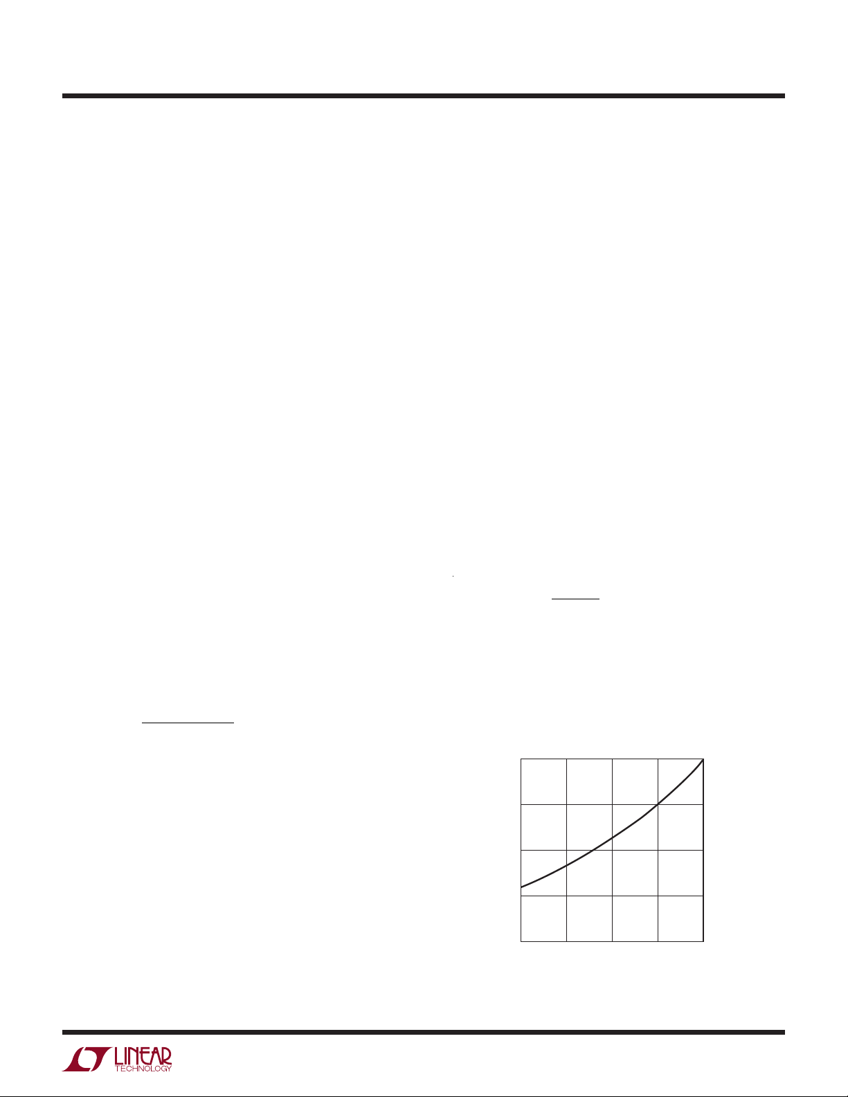
R
SENSE
=
V
SENSE(MAX)
1.3 • I
OUT(MAX)
applicaTions inForMaTion
LTC3810-5
The basic LTC3810-5 application circuit is shown on the
first page of this data sheet. External component selection
is primarily determined by the maximum input voltage and
load current and begins with the selection of the sense
resistance and power MOSFET switches. The LTC3810-5
uses either a sense resistor or the on-resistance of the
synchronous power MOSFET for determining the inductor
current. The desired amount of ripple current and operating
frequency largely determines the inductor value. Next, C
IN
is
selected for its ability to handle the large RMS current into
the converter and C
is chosen with low enough ESR to
OUT
meet the output voltage ripple and transient specification.
Finally, loop compensation components are selected to
meet the required transient/phase margin specifications.
Maximum Sense Voltage and V
RNG
Pin
Inductor current is determined by measuring the voltage across a sense resistance that appears between the
–
SENSE
is set by the voltage applied to the V
and SENSE+ pins. The maximum sense voltage
pin and is equal
RNG
to approximately:
V
SENSE(MAX)
= 0.173V
RNG
– 0.026
The current mode control loop will not allow the inductor
current valleys to exceed V
SENSE(MAX)/RSENSE
. In practice, one should allow some margin for variations in the
LTC3810-5 and external component values and a good
guide for selecting the sense resistance is:
An external resistive divider from INTVCC can be used
to set the voltage of the V
pin between 0.5V and 2V
RNG
resulting in nominal sense voltages of 60mV to 320mV.
Additionally, the V
pin can be tied to SGND or INTVCC
RNG
in which case the nominal sense voltage defaults to 95mV
or 215mV, respectively.
defined current limit, but adds cost and reduces efficiency.
Alternatively, one can eliminate the sense resistor and use
the bottom MOSFET as the current sense element by simply
+
connecting the SENSE
–
and SENSE
pin to the MOSFET source. This improves
pin to the lower MOSFET drain
efficiency, but one must carefully choose the MOSFET
on-resistance, as discussed below.
Power MOSFET Selection
The LTC3810-5 requires two external N-channel power
MOSFETs, one for the top (main) switch and one for the
bottom (synchronous) switch. Important parameters for
the power MOSFETs are the breakdown voltage BV
threshold voltage V
capacitance and maximum current I
, on-resistance R
(GS)TH
DS(MAX)
DS(ON)
.
,
DSS
, input
When the bottom MOSFET is used as the current sense
element, particular attention must be paid to its onresistance. MOSFET on-resistance is typically specified
with a maximum value R
DS(ON)(MAX)
at 25°C. In this case,
additional margin is required to accommodate the rise in
MOSFET on-resistance with temperature:
R
R
DS(ON)(MAX )
=
SENSE
ρ
T
The ρT term is a normalization factor (unity at 25°C)
accounting for the significant variation in on-resistance
temperature (see Figure 5) and typically varies
with
°
from 0.4%/
C to 1.0%/°C depending on the particular
MOSFET used.
2.0
1.5
1.0
+
Connecting the SENSE
and SENSE– Pins
The LTC3810-5 can be used with or without a sense resistor. When using a sense resistor, place it between the
source of the bottom MOSFET, M2 and PGND. Connect
+
the SENSE
and SENSE– pins to the top and bottom of
the sense resistor. Using a sense resistor provides a well
0.5
NORMALIZED ON-RESISTANCE
T
ρ
0
–50
0
JUNCTION TEMPERATURE (°C)
Figure 5. R
DS(ON)
50
100
vs Temperature
150
38105 F05
38105fd
15
Page 16

LTC3810-5
V
( )
IN
applicaTions inForMaTion
The most important parameter in high voltage applications
is breakdown voltage BV
. Both the top and bottom
DSS
MOSFETs will see full input voltage plus any additional
ringing on the switch node across its drain-to-source during its off-time and must be chosen with the appropriate
breakdown specification. The LTC3810-5 is designed to
be used with a 4.5V to 14V gate drive supply (DRV
for driving logic-level MOSFETs (V
GS(MIN)
For maximum efficiency, on-resistance R
capacitance should be minimized. Low R
≥ 4.5V).
DS(ON)
DS(ON)
pin)
CC
and input
minimizes
conduction losses and low input capacitance minimizes
transition losses. MOSFET input capacitance is a combination of several components but can be taken from the
typical “gate charge” curve included on most data sheets
(Figure 6).
V
IN
V
GS
MILLER EFFECT
a b
Q
C
MILLER
IN
= (QB – QA)/V
Figure 6. Gate Charge Characteristic
DS
V
+
V
+
V
GS
–
DS
–
38105 F06
The curve is generated by forcing a constant input current into the gate of a common source, current source
loaded stage and then plotting the gate voltage versus
time. The initial slope is the effect of the gate-to-source
and the gate-to-drain capacitance. The flat portion of the
curve is the result of the Miller multiplication effect of the
drain-to-gate capacitance as the drain drops the voltage
across the current source load. The upper sloping line is
due to the drain-to-gate accumulation capacitance and
the gate-to-source capacitance. The Miller charge (the
increase in coulombs on the horizontal axis from a to b
while the curve is flat) is specified for a given V
voltage, but can be adjusted for different V
multiplying by the ratio of the application V
specified V
values. A way to estimate the C
DS
DS
DS
drain
DS
voltages by
to the curve
term
MILLER
is to take the change in gate charge from points a and b
on a manufacturers data sheet and divide by the stated
voltage specified. C
V
DS
is the most important se-
MILLER
lection criteria for determining the transition loss term in
the top MOSFET but is not directly specified on MOSFET
data sheets. C
and COS are specified sometimes but
RSS
definitions of these parameters are not included.
When the controller is operating in continuous mode the
duty cycles for the top and bottom MOSFETs are given by:
Main Switch Duty Cycle =
Synchronous Switch Duty Cycle=
OUT
V
IN
– V
V
IN
OUT
V
IN
The power dissipation for the main and synchronous
MOSFETs at maximum output current are given by:
V
P
TOP
OUT
=
V
IN
I
2
V
IN
⎡
⎢
V
⎢
CC
⎣
– V
V
P
BOT
IN
=
V
where ρT is the temperature dependency of R
I
MAX
MAX
2
– V
OUT
(RDR)(C
1
TH(IL)
(I
2
(ρT)R
MAX
DS(ON)
MILLER
1
+
V
TH(IL)
)2(ρT)R
+
) •
⎤
(f)
⎥
⎥
⎦
DS(0N)
DS(ON)
, RDR
is the effective top driver resistance (approximately 2Ω at
= V
V
GS
in drain potential in the particular application. V
), VIN is the drain potential and the change
MILLER
TH(IL)
is
the data sheet specified typical gate threshold voltage
specified in the power MOSFET data sheet at the specified
drain current. C
is the calculated capacitance using
MILLER
the gate charge curve from the MOSFET data sheet and
the technique described above.
2
Both MOSFETs have I
R losses while the topside N-channel
equation incudes an additional term for transition losses,
which peak at the highest input voltage. For high input
voltage low duty cycle applications that are typical for the
LTC3810-5, transition losses are the dominate loss term and
therefore using higher R
device with lower C
DS(ON)
MILLER
usually provides the highest efficiency. The synchronous
MOSFET losses are greatest at high input voltage when
the top switch duty factor is low or during a short-circuit
when the synchronous switch is on close to 100% of
38105fd
16
Page 17
applicaTions inForMaTion
LTC3810-5
the period. Since there is no transition loss term in the
synchronous MOSFET, optimal efficiency is obtained by
minimizing R
—by using larger MOSFETs or paral-
DS(ON)
leling multiple MOSFETs.
Multiple MOSFETs can be used in parallel to lower
R
and meet the current and thermal requirements
DS(ON)
if desired. The LTC3810-5 contains large low impedance
drivers capable of driving large gate capacitances without
significantly slowing transition times. In fact, when driving MOSFETs with very low gate charge, it is sometimes
helpful to slow down the drivers by adding small gate
resistors (10Ω or less) to reduce noise and EMI caused
by the fast transitions.
Operating Frequency
The choice of operating frequency is a tradeoff between
efficiency and component size. Low frequency operation
improves efficiency by reducing MOSFET switching losses
but requires larger inductance and/or capacitance in order
to maintain low output ripple voltage.
The operating frequency of LTC3810-5 applications is
determined implicitly by the one-shot timer that controls
the on-time, t
is set by the current out of the I
the V
pin according to:
ON
tON=
, of the top MOSFET switch. The on-time
ON
pin and the voltage at
ON
V
VON
(76pF)
I
ION
Tying a resistor RON from VIN to the ION pin yields an
on-time inversely proportional to V
. For a step-down
IN
converter, this results in approximately constant frequency
operation as the input supply varies:
V
f =
V
OUT
• RON(76pF)
VON
[HZ]
To hold frequency constant during output voltage changes,
tie the V
when V
pin to V
ON
> 2.4V. The VON pin has internal clamps that
OUT
or to a resistive divider from V
OUT
OUT
limit its input to the one-shot timer. If the pin is tied below
0.7V, the input to the one-shot is clamped at 0.7V. Similarly,
if the pin is tied above 2.4V, the input is clamped at 2.4V.
In high V
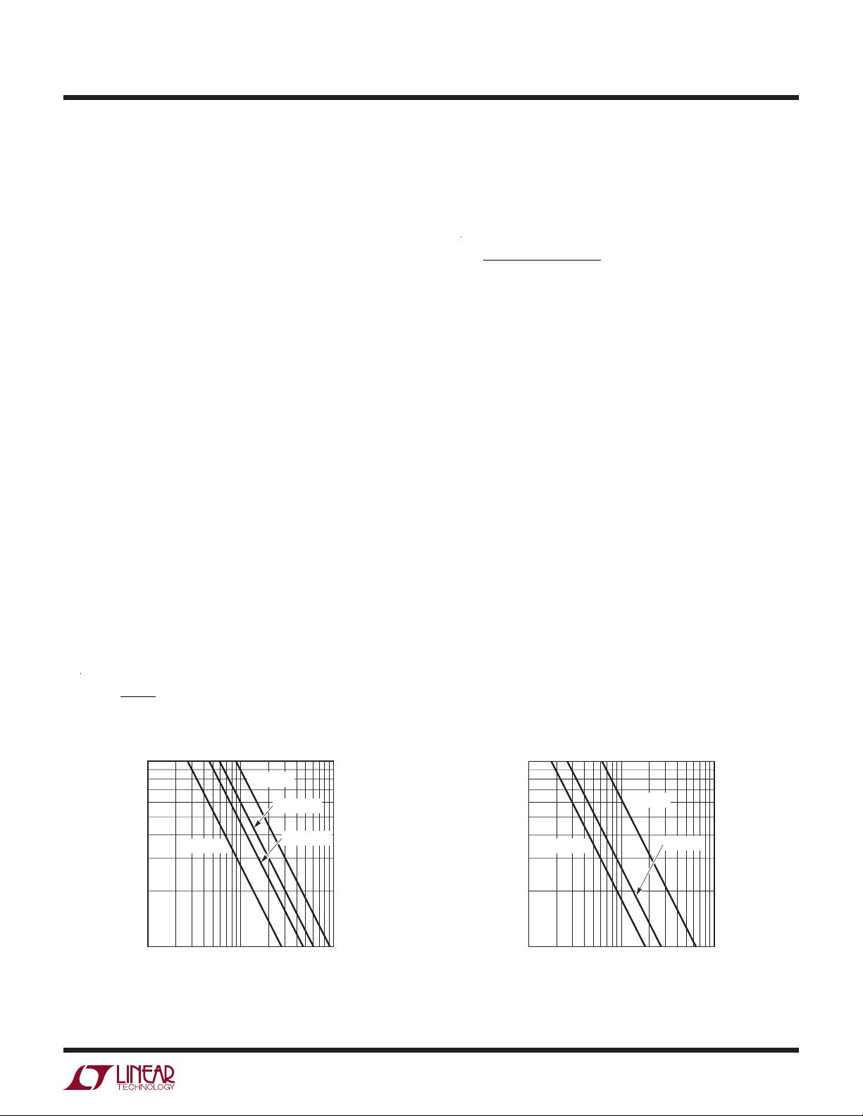
and 7b show how R
applications, tie VON to INTVCC. Figures 7a
OUT
relates to switching frequency for
ON
several common output voltages.
Changes in the load current magnitude will cause frequency shift. Parasitic resistance in the MOSFET switches
and inductor reduce the effective voltage across the
inductance, resulting in increased duty cycle as the load
current increases. By lengthening the on-time slightly as
current increases, constant frequency operation can be
maintained. This is accomplished with a resistive divider
from the I
pin to the VON pin and V
TH
. The values
OUT
required will depend on the parasitic resistances in the
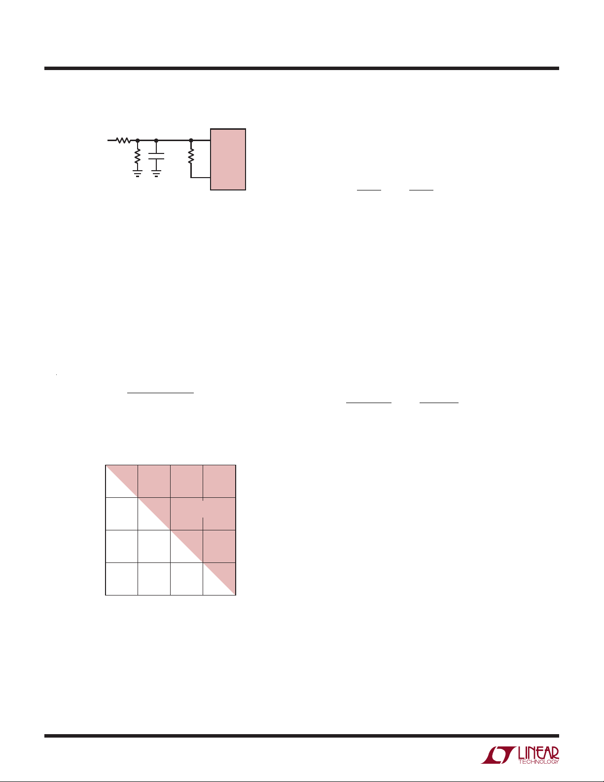
specific application. A good starting point is to feed about
25% of the voltage change at the I
as shown in Figure 8. Place capacitance on the V
to filter out the I
variations at the switching frequency.
TH
pin to the VON pin
TH
ON
pin
1000
V
= 5V
OUT
V
= 3.3V
OUT
V
= 2.5V
V
= 1.5V
OUT
SWITCHING FREQUENCY (kHz)
100
10
Figure 7a. Switching Frequency vs RON (VON = 0V) Figure 7b. Switching Frequency vs RON (VON = INTVCC)
100 1000
RON (kΩ)
OUT
38105 F07a
1000
V
= 3.3V
OUT
SWITCHING FREQUENCY (kHz)
100
10
RON (kΩ)
V
= 12V
OUT
V
= 5V
OUT
100 1000
38105 F07b
38105fd
17
Page 18
LTC3810-5
ON
applicaTions inForMaTion
R
VON1
5.5V
100k
CC
R
VON2
30k
C
VON
0.01µF
100k
V
ON
LTC3810-5
I
TH
38105 F08
INTV
Figure 8. Correcting Frequency Shift with Load Current Changes
Inductor Selection
Given the desired input and output voltages, the inductor value and operating frequency determine the ripple
current:
⎛
ΔI
=
L
⎜
⎝
V
OUT
f L
⎞
⎛
1−
⎟
⎜
⎝
⎠
V
OUT
V
IN
⎞
⎟
⎠
Minimum Off-Time and Dropout Operation
The minimum off-time t
OFF(MIN)
is the smallest amount of
time that the LTC3810-5 is capable of turning on the bottom MOSFET, tripping the current comparator and turning
the MOSFET back off. This time is generally about 250ns.
The minimum off-time limit imposes a maximum duty
cycle of t
/(tON + t
ON
OFF(MIN)
). If the maximum duty cycle
is reached, due to a dropping input voltage for example,
then the output will drop out of regulation. The minimum
input voltage to avoid dropout is:
V
IN(MIN)
= V
tON+ t
OUT
OFF(MIN)
t
A plot of maximum duty cycle vs frequency is shown in
Figure 9.
2.0
1.5
1.0
DROPOUT
REGION
Lower ripple current reduces core losses in the inductor,
ESR losses in the output capacitors and output voltage
ripple. Highest efficiency operation is obtained at low
frequency with small ripple current. However, achieving
this requires a large inductor. There is a tradeoff between
component size, efficiency and operating frequency.
A reasonable starting point is to choose a ripple current
that is about 40% of I
OUT(MAX)
occurs at the highest V
IN
. The largest ripple current
. To guarantee that ripple current
does not exceed a specified maximum, the inductance
should be chosen according to:
⎛
L =
V
⎜
fΔI
L(MAX)
⎝
OUT
⎞
⎛
V
1−
⎟
⎜
V
⎝
⎠
IN(MAX)
OUT
⎞
⎟
⎠
Once the value for L is known, the type of inductor must
be selected. High efficiency converters generally cannot
afford the core loss found in low cost powdered iron cores,
forcing the use of more expensive ferrite, molypermalloy
®
or Kool Mµ
cores. A variety of inductors designed for
high current, low voltage applications are available from
manufacturers such as Sumida, Panasonic, Coiltronics,
Coilcraft and Toko.
0.5
SWITCHING FREQUENCY (MHz)
Schottky Diode D1 Selection
The Schottky diode D1 shown in the front page schematic
0
0 0.25 0.50 0.75
DUTY CYCLE (V
Figure 9. Maximum Switching Frequency vs Duty Cycle
OUT/VIN
)
1.0
38105 F09
conducts during the dead time between the conduction
of the power MOSFET switches. It is intended to prevent
the body diode of the bottom MOSFET from turning on
and storing charge during the dead time, which can cause
a modest (about 1%) efficiency loss. The diode can be
rated for about one-half to one-fifth of the full load current
since it is on for only a fraction of the duty cycle. In order
for the diode to be effective, the inductance between it
38105fd
18
Page 19

applicaTions inForMaTion
LTC3810-5
and the bottom MOSFET must be as small as possible,
mandating that these components be placed adjacently.
The diode can be omitted if the efficiency loss is tolerable.
Input Capacitor Selection
In continuous mode, the drain current of the top MOSFET
is approximately a square wave of duty cycle V
OUT/VIN
which must be supplied by the input capacitor. To prevent
large input transients, a low ESR input capacitor sized for
the maximum RMS current is given by:
I
CIN(RMS)≅IO(MAX)
V
OUT
V
IN
V
IN
⎜
V
⎝
OUT
⎛
This formula has a maximum at VIN = 2V
I
/2. This simple worst-case condition is commonly
O(MAX)
– 1
⎞
⎟
⎠
1/2
OUT
, where I
RMS
=
used for design because even significant deviations do not
offer much relief. Note that the ripple current ratings from
capacitor manufacturers are often based on only 2000
hours of life. This makes it advisable to further derate
the capacitor or to choose a capacitor rated at a higher
temperature than required. Several capacitors may also
be placed in parallel to meet size or height requirements
in the design.
Because tantalum and OS-CON capacitors are not available
in voltages above 30V, ceramics or aluminum electrolytics
must be used for regulators with input supplies above 30V.
Ceramic capacitors have the advantage of very low ESR
and can handle high RMS current, but ceramics with high
voltage ratings (> 50V) are not available with more than
a few microfarads of capacitance. Furthermore, ceramics have high voltage coefficients which means that the
capacitance values decrease even more when used at the
rated voltage. X5R and X7R type ceramics are recommended for their lower voltage and temperature coefficients. Another consideration when using ceramics is
their high Q which, if not properly damped, may result in
excessive voltage stress on the power MOSFETs. Aluminum electrolytics have much higher bulk capacitance,
but they have higher ESR and lower RMS current ratings.
A good approach is to use a combination of aluminum
electrolytics for bulk capacitance and ceramics for low ESR
and RMS current. If the RMS current cannot be handled
by the aluminum capacitors alone, when used together,
the percentage of RMS current that will be supplied by the
aluminum capacitor is reduced to approximately:
% I
RMS,ALUM
where R
≈
is the ESR of the aluminum capacitor and C
ESR
1
1+ (8fCR
ESR
2
)
• 100%
is the overall capacitance of the ceramic capacitors. Using
an aluminum electrolytic with a ceramic also helps damp
the high Q of the ceramic, minimizing ringing.
Output Capacitor Selection
The selection of C
is primarily determined by the ESR
OUT
required to minimize voltage ripple. The output ripple
(DV
) is approximately equal to:
OUT
⎛
ΔV
≤ ΔILESR +
OUT
⎜
⎝
8fC
1
OUT
⎞
⎟
⎠
Since DIL increases with input voltage, the output ripple
is highest at maximum input voltage. ESR also has a significant effect on the load transient response. Fast load
transitions at the output will appear as voltage across the
ESR of C
until the feedback loop in the LTC3810-5 can
OUT
change the inductor current to match the new load current
value. Typically, once the ESR requirement is satisfied the
capacitance is adequate for filtering and has the required
RMS current rating.
Manufacturers such as Nichicon, Nippon Chemi-Con
and Sanyo should be considered for high performance
throughhole capacitors. The OS-CON (organic semiconductor dielectric) capacitor available from Sanyo has the
lowest product of ESR and size of any aluminum electrolytic at a somewhat higher price. An additional ceramic
capacitor in parallel with OS-CON capacitors is recommended to reduce the effect of their lead inductance.
In surface mount applications, multiple capacitors placed
in parallel may be required to meet the ESR, RMS current
handling and load step requirements. Dry tantalum, special
polymer and aluminum electrolytic capacitors are available
in surface mount packages. Special polymer capacitors
offer very low ESR but have lower capacitance density
38105fd
19
Page 20

LTC3810-5
applicaTions inForMaTion
than other types. Tantalum capacitors have the highest
capacitance density but it is important to only use types
that have been surge tested for use in switching power
supplies. Several excellent surge-tested choices are the
AVX, TPS and TPSV or the KEMET T510 series. Aluminum
electrolytic capacitors have significantly higher ESR, but
can be used in cost-driven applications providing that
consideration is given to ripple current ratings and long
term reliability. Other capacitor types include Panasonic
SP and Sanyo POSCAPs.
Output Voltage
The LTC3810-5 output voltage is set by a resistor divider
according to the following formula:
V
⎛
= 0.8V 1+
OUT
⎜
⎝
⎞
R
FB1
⎟
R
⎠
FB2
The external resistor divider is connected to the output as
shown in the Functional Diagram, allowing remote voltage
sensing. The resultant feedback signal is compared with
the internal precision 800mV voltage reference by the
error amplifier. The internal reference has a guaranteed
tolerance of less than ±1%. Tolerance of the feedback
resistors will add additional error to the output voltage.
0.1% to 1% resistors are recommended.
Input Voltage Undervoltage Lockout
A resistor divider connected from the input supply to the
UVIN pin (see Functional Diagram) is used to program the
input supply undervoltage lockout thresholds. When the
rising voltage at UVIN reaches 0.88V the LTC3810 turns
on, and when the falling voltage at UVIN drops below 0.8V,
the LTC3810 is shut down—providing 10% hysterisis.
The input voltage UVLO thresholds are set by the resistor
divider according to the following formulas:
V
IN,FALLING
= 0.8V (1 + R
UV1/RUV2
)
and
Top MOSFET Driver Supply (C
An external bootstrap capacitor, C
, DB)
B
, connected to the
B
BOOST pin supplies the gate drive voltage for the topside
MOSFET. This capacitor is charged through diode D
when the switch node is low. When the top MOSFET
DRV
CC
turns on, the switch node rises to V
rises to approximately V
+ INTVCC. The boost capacitor
IN
and the BOOST pin
IN
from
B
needs to store about 100 times the gate charge required
by the top MOSFET. In most applications 0.1µF to 0.47µF ,
X5R or X7R dielectric capacitor is adequate.
The reverse breakdown of the external diode, D
greater than V
IN(MAX)
. Another important consideration for
, must be
B
the external diode is the reverse recovery and reverse leakage, either of which may cause excessive reverse current
to flow at full reverse voltage. If the reverse current times
reverse voltage exceeds the maximum allowable power
dissipation, the diode may be damaged. For best results,
use an ultrafast recovery diode such as the MMDL770T1.
Bottom MOSFET Driver Return Supply (BGRTN)
The bottom gate driver, BG, switches from DRV
CC
to
BGRTN where BGRTN can be a voltage between ground
and –5V. Why not just keep it simple and always connect
BGRTN to ground? In high voltage switching converters,
the switch node dV/dt can be many volts/ns, which will
pull up on the gate of the bottom MOSFET through its
Miller capacitance. If this Miller current, times the internal
gate resistance of the MOSFET plus the driver resistance,
exceeds the threshold of the FET, shoot-through will occur. By using a negative supply on BGRTN, the BG can be
pulled below ground when turning the bottom MOSFET off.
This provides a few extra volts of margin before the gate
reaches the turn-on threshold of the MOSFET. Be aware
that the maximum voltage difference between DRV
BGRTN is 14V. If, for example, V
voltage on DRV
pin is now 12V instead of 14V.
CC
IC/MOSFET Driver Supplies (INTV
= –2V, the maximum
BGRTN
and DRVCC)
CC
CC
and
V
IN,RISING
= 0.88V (1 + R
UV1/RUV2
)
If input supply undervoltage lockout is not needed, it can
be disabled by connecting UVIN to INTV
CC
.
20
The LTC3810-5 drivers are supplied from the DRV
CC
and BOOST pins (see Figure 2), which have an absolute
maximum voltage of 14V. Since the main supply voltage,
38105fd
Page 21
( )
applicaTions inForMaTion
LTC3810-5
VIN is typically much higher than 14V a separate supply
for the IC power (INTV
) and driver power (DRVCC) must
CC
be used. The LTC3810-5 has integrated bias supply control circuitry that allows the IC/driver supply to be easily
generated from V
and/or V
IN
with minimal external
OUT
components. There are four ways to do this as shown in
the simplified schematics of Figure 3 and explained in the
following sections.
Using the Linear Regulator for INTV
/DRVCC Supply
CC
In Mode 1, a small external SOT23 MOSFET, controlled
by the NDRV pin, is used to generate a 5.5V start-up
supply from V
. The small SOT23 package can be used
IN
because the NMOS is on continuously only during the brief
start-up period. As soon as the output voltage reaches
4.7V, the LTC3810-5 turns off the external NMOS and the
LTC3810-5 regulates the 5.5V supply from the EXTV
pin (connected to V
OUT
or a V
derived boost network)
OUT
CC
through an internal low dropout regulator. For this mode to
work properly, EXTV
< 15V. If V
< 4.7V, a charge pump or extra winding can
OUT
be used to raise EXTV
must be in the range 4.7V < EXTV
CC
to the proper voltage, or alter-
CC
CC
natively, Mode 2 should be used as explained later in this
section. If V
minimum 4.5V threshold, the MOSFET connected to V
is shorted or otherwise goes below the
OUT
IN
is turned back on to maintain the 5.5V supply. However if
the output cannot be brought up within a timeout period,
the drivers are turned off to prevent the SOT23 MOSFET
from overheating. Soft-start cycles are then attempted at
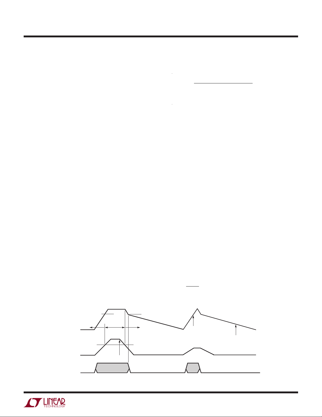
low duty cycle intervals to try to bring the output back up
(see Figure 10). This fault timeout operation is enabled
by choosing the choosing R
such that the resistor
NDRV
current I
is greater than 270µA by using the follow-
NDRV
ing formulas:
P
R
NDRV
MOSFET(MAX )/ICC
≤
270µA
− V
TH
where
ICC=(f) Q
G(TOP)+QG(BOTTOM)
+ 3mA
and VTH is the threshold voltage of the MOSFET.
The value of R
IN(MIN)
INTVCC(MIN)
= V
V
where V
also affects the V
NDRV
INTVCC(MIN)
is normally 4.5V for driving logic-level
MOSFETs. If minimum V
reducing R
and/or using a Darlington NPN instead
NDRV
of an NMOS to reduce V
When using R
equal to the computed value, the
NDRV
+ (40µA) R
is not low enough, consider
IN
to ~1.4V.
T
as follows:
IN(MIN)
+VT (1)
NDRV
LTC3810-5 will enable the low duty cycle soft-start retries only when the desired maximum power dissipation,
P
MOSFET(MAX)
, in the MOSFET is exceeded and leave the
drivers on continuously otherwise. The shutoff/restart
times are a function of the TRACK/SS capacitor value.
The external NMOS for the linear regulator should be a
standard 3V threshold type (i.e., not a logic-level threshold).
The rate of charge of INTV
from 0V to 5.5V is controlled
CC
by the LTC3810-5 to be approximately 75µs regardless
of the size of the capacitor connected to the INTV
CC
pin.
The charging current for this capacitor is approximately:
⎛
IC=
⎜
⎝
5.5V
75µs
⎞
C
⎟
⎠
INTVCC
SS/TRACK
V
OUT
TG/BG
FAULT TIMEOUT
ENABLED
DRIVER POWER
FROM V
IN
START-UP
SHORT-CIRCUIT EVENT START-UP INTO SHORT-CIRCUIT
DRIVER POWER
FROM V
OUT
Figure 10. Fault Timeout Operation
DRIVER OFF THRESHOLD
DRIVER POWER
FROM V
IN
EXTV
UV THRESHOLD
CC
I
SS/TRACK
= 1.4µA (SOURCE)
I
SS/TRACK
= 0.1µA (SINK)
38105 F10
38105fd
21
Page 22

LTC3810-5
( )
( )
( )
applicaTions inForMaTion
The safe operating area (SOA) for the external NMOS
should be chosen so that capacitor charging does not
damage the NMOS. Excessive values of capacitor are
unnecessary and should be avoided. Typically values in
the 1µF to 10µF work well.
One more design requirement for this mode is the minimum
soft-start capacitor value. The fault timeout is enabled
when SS/TRACK voltage is greater than 4V. This gives the
power supply time to bring the output up before it starts
the timeout sequence. To prevent timeout sequence from
starting prematurely during start-up, a minimum C
is necessary to ensure that V
SS/TRACK
< 4V until V
value
SS
EXTVCC
> 4.7V. To ensure this, choose:
> C
C
SS
Mode 2 should be used if V
EXTV
CC
• (2.3 • 10–6)/I
OUT
OUT(MAX)
is outside of the 4.7V <
OUT
< 15V operating range and the extra complexity
of a charge pump or extra inductor winding is not wanted
to boost this voltage above 4.7V. In this mode, EXTV
CC
is
grounded and the NMOS is chosen to handle the worstcase power dissipation:
P
MOSFET
= V
IN(MAX)
⎡
f
Q
⎣
G(TOP)
+ Q
G(BOTTOM)
+ 3mA
⎤
⎦
To operate properly, the fault timeout operation must be
disabled by choosing
by the driver current I
up, C
INTVCC/CDRVCC
the EXTV
4.7V before C
voltage reaches the switchover threshold of
CC
INTVCC/CDRVCC
. In order to ensure proper start-
G
must be chosen large enough so that
discharges below the falling
UV threshold of 4V. This is ensured if:
C
INTVCC
I
G
Where IG is the gate drive current = (f)(Q
Q
G(BOTTOM)
selected by V
For R
+ C
DRVCC
⎛
• largerof
⎜
⎝
) and I
RNG
PULLUP
, the value should fall in the following range
>
C
OUT
I
MAX
MAX
5.5 • 10
or
is the maximum inductor current
5
V
OUT(REG)
• C
SS
⎞
⎟
⎠
.
G(TOP)
+
to ensure proper start-up:
Min R
Max R
PULLUP
PULLUP
> (V
< (V
IN(MAX)
IN(MIN)
– 14V)/I
– 9V)/I
CCSR
Q,SHUTDOWN
Using an External Supply Connected to the INTVCC/
Pins
DRV
CC
If an external supply is available between 4.5V and 14V,
the supply can be connected directly to the INTV
pins. In this mode, INTV
, EXTVCC and NDRV must be
CC
/DRVCC
CC
shorted together.
NDRV
> (V
IN(MAX)
R
If the required R
for V
(see Equation 1), fault timeout operation can
IN(MIN)
also be disabled by connecting a 500k to 1Meg resistor
from SS/TRACK pin to INTV
– 5.5V – VTH)/270µA
value results in an unacceptable value
NDRV
.
CC
INTV
/DRVCC Supply and the EXTVCC Connection
CC
The LTC3810-5 contains an internal low dropout regulator
to produce the 5.5V INTV
pin voltage. This regulator turns on when the EXTV
is above 4.7V and remains on until EXTV
/DRVCC supply from the EXTVCC
CC
drops below
CC
CC
pin
4.45V. This allows the IC/MOSFET power to be derived
Using Trickle Charge Mode
Trickle charge mode is selected by shorting NDRV and
INTV
and connecting EXTVCC to V
CC
. Trickle charge
OUT
mode has the advantage of not requiring an external
MOSFET but takes longer to start up due to slow charge
up of C
• R
PULLUP
DRV
CC
and C
INTVCC
• C
DRVCC
capacitor values to hold up the supply voltage dur-
ing start-up. Once the INTV
DRVCC
through R
PULLUP
(t
DELAY
= 0.77
) and usually requires larger INTVCC/
/DRVCC voltage reaches the
CC
trickle charge UV threshold of 9V, the drivers will turn on
and start discharging C
INTVCC/CDRVCC
at a rate determined
from the output or an output derived boost network during
normal operation and from the external NMOS from V
during start-up or short-circuit. Using the EXTV
CC
IN
pin in
this way results in significant efficiency gains compared
to what would be possible when deriving this power
continuously from the typically much higher V
The EXTV
connection also allows the power supply to
CC
voltage.
IN
be configured in trickle charge mode in which it starts up
38105fd
IN
with a high valued “bleed” resistor connected from V
to INTV
the output rises above 4.7V the internal EXTV
to charge up the INTVCC capacitor. As soon as
CC
regulator
CC
22
Page 23

( )
applicaTions inForMaTion
LTC3810-5
takes over before the INTVCC capacitor discharges below
the UV threshold. When the EXTV
the EXTV
pin can supply up to 50mA RMS. Do not ap-
CC
ply more than 15V to the EXTV
summarizes the possible connections for EXTV
1. EXTV
grounded. This connection will require INTVCC
CC
regulator is active,
CC
pin. The following list
CC
:
CC
to be powered continuously from an external NMOS
from V
resulting in an efficiency penalty as high as
IN
10% at high input voltages.
2. EXTV
connected directly to V
CC
connection for 4.7V < V
OUT
. This is the normal
OUT
< 15V and provides the
highest efficiency. The power supply will start up using
an external NMOS or a bleed resistor until the output
supply is available.
3. EXTV
If V
connected to an output-derived boost network.
CC
< 4.7V. The low voltage output can be boosted
OUT
using a charge pump or flyback winding to greater
than 4.7V.
4. EXTV
nection for EXTV
supply where the external supply is 4.5V < V
connected to INTVCC. This is the required con-
CC
if INTVCC is connected to an external
CC
< 15V.
EXT
Applications using large MOSFETs with a high input
voltage and high frequency of operation may result in a
large EXTV
pin current. Due to the LTC3810-5 thermally
CC
enhanced package, maximum junction temperature will
rarely be exceeded, however, it is good design practice
to verify that the maximum junction temperature rating
and RMS current rating are within the maximum limits.
Typically, most of the EXTV
current consists of the
CC
MOSFET gates current. In continuous mode operation,
this EXTV
I
EXTVCC
current is:
CC
= f Q
G(TOP)+QG(BOTTOM)
+ 3mA < 50mA
The junction temperature can be estimated from the
equations given in Note 2 of the Electrical Characteristics
as follows:
= TA + I
T
J
The calculated T
• (V
EXTVCC
J
EXTVCC
should be <125°C for E- and I-grade
– V
INTVCC
)(34°C/W)
or < 150°C for H-grade. If absolute maximum ratings are
exceeded, consider using an external supply connected
directly to the INTV
CC
pin.
FEEDBACK LOOP/COMPENSATION
Feedback Loop Types
In a typical LTC3810-5 circuit, the feedback loop consists of the modulator, the output filter and load, and the
feedback amplifier with its compensation network. All of
these components affect loop behavior and must be accounted for in the loop compensation. The modulator and
output filter consists of the internal current comparator,
the output MOSFET drivers and the external MOSFETs,
inductor and output capacitor. Current mode control
eliminates the effect of the inductor by moving it to the
inner loop, reducing it to a first order system. From a
feedback loop point of view, it looks like a linear voltage
controlled current source from I
equal to (I
MAXROUT
)/1.2V. It has fairly benign AC behavior
TH
to V
and has a gain
OUT
at typical loop compensation frequencies with significant
phase shift appearing at half the switching frequency. The
external output capacitor and load cause a first order roll
off at the output at the R
OUTCOUT
pole frequency, with
the attendant 90° phase shift. This roll off is what filters
the PWM waveform, resulting in the desired DC output
voltage. The output capacitor also contributes a zero at
the C
OUTRESR
frequency which adds back the 90° phase
and cancels the first order roll off.
So far, the AC response of the loop is pretty well out of the
user’s control. The modulator is a fundamental piece of
the LTC3810-5 design and the external output capacitor is
usually chosen based on the regulation and load current
requirements without considering the AC loop response.
The feedback amplifier, on the other hand, gives us a
handle with which to adjust the AC response. The goal is
to have 180° phase shift at DC (so the loop regulates), and
something less than 360° phase shift (preferably about
300°) at the point that the loop gain falls to 0dB, i.e., the
crossover frequency, with as much gain as possible at
frequencies below the crossover frequency. Since the
modulator/output filter is a first order system with maximum of 90° phase shift (at frequencies below f
/4) and
SW
the feedback amplifier adds another 90° of phase shift,
some phase boost is required at the crossover frequency
to achieve good phase margin. If the ESR zero is below the
crossover frequency, this zero may provide enough phase
boost to achieve the desired phase margin and the only
38105fd
23
Page 24

LTC3810-5
applicaTions inForMaTion
requirement of the compensation will be to guarantee that
the gain is below zero at frequencies above f
/4. If the
SW
ESR zero is above the crossover frequency, the feedback
amplifier will probably be required to provide phase boost.
For most LTC3810-5 applications, Type 2 compensation will
provide enough phase boost; however some applications
where high bandwidth is required with low ESR ceramics
and lots of bulk capacitance, Type 3 compensation may
be necessary to provide additional phase boost.
The two types of compensation networks, “Type 2” and
“Type 3” are shown in Figures 11 and 12. When component values are chosen properly, these networks provide
a “phase bump” at the crossover frequency. Type 2 uses
a single pole-zero pair to provide up to about 60° of phase
boost while Type 3 uses two poles and two zeros to provide
up to 150° of phase boost.
C2
IN
R
FB1
FB
R
FB2
V
REF
C1
R2
–
OUT
+
GAIN (dB)
GAIN
0
PHASE
–6dB/OCT
Figure 11. Type 2 Schematic and Transfer Function
IN
C3
R
R3
FB1
FB
R
FB2
V
REF
C2
C1
R2
–
+
OUT
GAIN (dB)
GAIN
0
–6dB/OCT
–6dB/OCT
+6dB/OCT –6dB/OCT
PHASE
PHASE (DEG)
FREQ
–90
–180
–270
–360
38105 F11
PHASE (DEG)
FREQ
–90
–180
–270
–360
38105 F12
Feedback Component Selection
Selecting the R and C values for a typical Type 2 or Type 3
loop is a nontrivial task. The applications shown in this
data sheet show typical values, optimized for the power
components shown. They should give acceptable performance with similar power components, but can be way off if
even one major power component is changed significantly.
Applications that require optimized transient response will
require recalculation of the compensation values specifically
for the circuit in question. The underlying mathematics are
complex, but the component values can be calculated in
a straightforward manner if we know the gain and phase
of the modulator at the crossover frequency.
Modulator gain and phase can be obtained in one of
three ways: measured directly from a breadboard, or if
the appropriate parasitic values are known, simulated or
generated from the modulator transfer function. Measurement will give more accurate results, but simulation
or transfer function can often get close enough to give
a working system. To measure the modulator gain and
phase directly, wire up a breadboard with an LTC3810-5
and the actual MOSFETs, inductor and input and output
capacitors that the final design will use. This breadboard
should use appropriate construction techniques for high
speed analog circuitry: bypass capacitors located close
to the LTC3810-5, no long wires connecting components,
appropriately sized ground returns, etc. Wire the feedback
amplifier with a 0.1µF feedback capacitor from I
and a 10k to 100k resistor from V
bias resistor (R
voltage. Disconnect R
) as required to set the desired output
FB2
from ground and connect it to
FB2
to FB. Choose the
OUT
to FB
TH
a signal generator or to the source output of a network
analyzer to inject a test signal into the loop. Measure the
gain and phase from the I
pin to the output node at the
TH
positive terminal of the output capacitor. Make sure the
analyzer’s input is AC coupled so that the DC voltages
present at both the I
and V
TH
nodes don’t corrupt the
OUT
measurements or damage the analyzer.
Figure 12. Type 3 Schematic and Transfer Function
24
If breadboard measurement is not practical, a SPICE
simulation can be used to generate approximate gain/
phase curves. Plug the expected capacitor, inductor and
MOSFET values into the following SPICE deck and generate an AC plot of V
OUT/VITH
with gain in dB and phase in
38105fd
Page 25

( )
applicaTions inForMaTion
degrees. Refer to your SPICE manual for details of how
to generate this plot.
LTC3810-5
*3810-5 modulator gain/phase
*2006 Linear Technology
*this file simulates a simplified model of
*the LTC3810-5 for generating a v(out)/
v(ith)
*bode plot
.param rdson=.0135 ;MOSFET rdson
.param Vrng=2 ;use 1.4 for INTVCC and
0.7 for ground
.param vsnsmax={0.173*Vrng-0.026}
.param Imax={vsnsmax/rdson}
.param DL=4 ;inductor ripple current
*inductor current
gl out 0 value={(v(ith)-1.2)*Imax/1.2+DL/2}
*output cap
cout out out2 270u ;capacitor value
resr out2 0 0.018 ;capacitor ESR
*load
Rout out 0 2 ; load resistor
GAIN
0 0
GAIN (dB)
PHASE
FREQUENCY (Hz)
Figure 13. Transfer Function of Buck Modulator
38105 F13
PHASE (DEG)
–90
–180
(PHASE, in degrees) at this point. The desired feedback
amplifier gain will be –GAIN to make the loop gain at 0dB
at this frequency. Now calculate the needed phase boost,
assuming 60° as a target phase margin:
BOOST = – (PHASE + 30°)
If the required BOOST is less than 60°, a Type 2 loop can
be used successfully, saving two external components.
BOOST values greater than 60° usually require Type 3
loops for satisfactory performance.
vstim ith 0 0 ac 1 ;ac stimulus
.ac dec 100 100 10meg
.probe
.end
Mathematical software such as MATHCAD or MATLAB
can also be used to generate plots using the following
transfer function of the modulator:
H(s) =
⎛
V
SENSE(MAX)
⎜
1.2 • R
⎝
s = j2πf
DS(ON)
⎞
⎟
⎠
⎛
1+ s • R
•
⎜
⎝
ESR
1+ s • RL• C
• C
OUT
OUT
⎞
⎟
⎠
• R
(2)
L
With the gain/phase plot in hand, a loop crossover frequency can be chosen. Usually the curves look something
like Figure 13. Choose the crossover frequency about 25%
of the switching frequency for maximum bandwidth. Although it may be tempting to go beyond f
/4, remember
SW
that significant phase shift occurs at half the switching
frequency that isn’t modeled in the above H(s) equation
and PSPICE code. Note the gain (GAIN, in dB) and phase
Finally, choose a convenient resistor value for R
FB1
(10k is
usually a good value). Now calculate the remaining values:
(K is a constant used in the calculations)
f = chosen crossover frequency
G = 10
(GAIN/20)
(this converts GAIN in dB to G in
absolute gain)
TYPE 2 Loop:
K = tan
C2=
2π • f • G • K •R
⎛
⎜
⎝
2
1
+ 45°
FB1
⎞
⎟
⎠
BOOST
C1=C2 K2−1
R2=
K
2π • f • C1
V
=
V
REF(RFB1
OUT
R
FB2
− V
)
REF
38105fd
25
Page 26
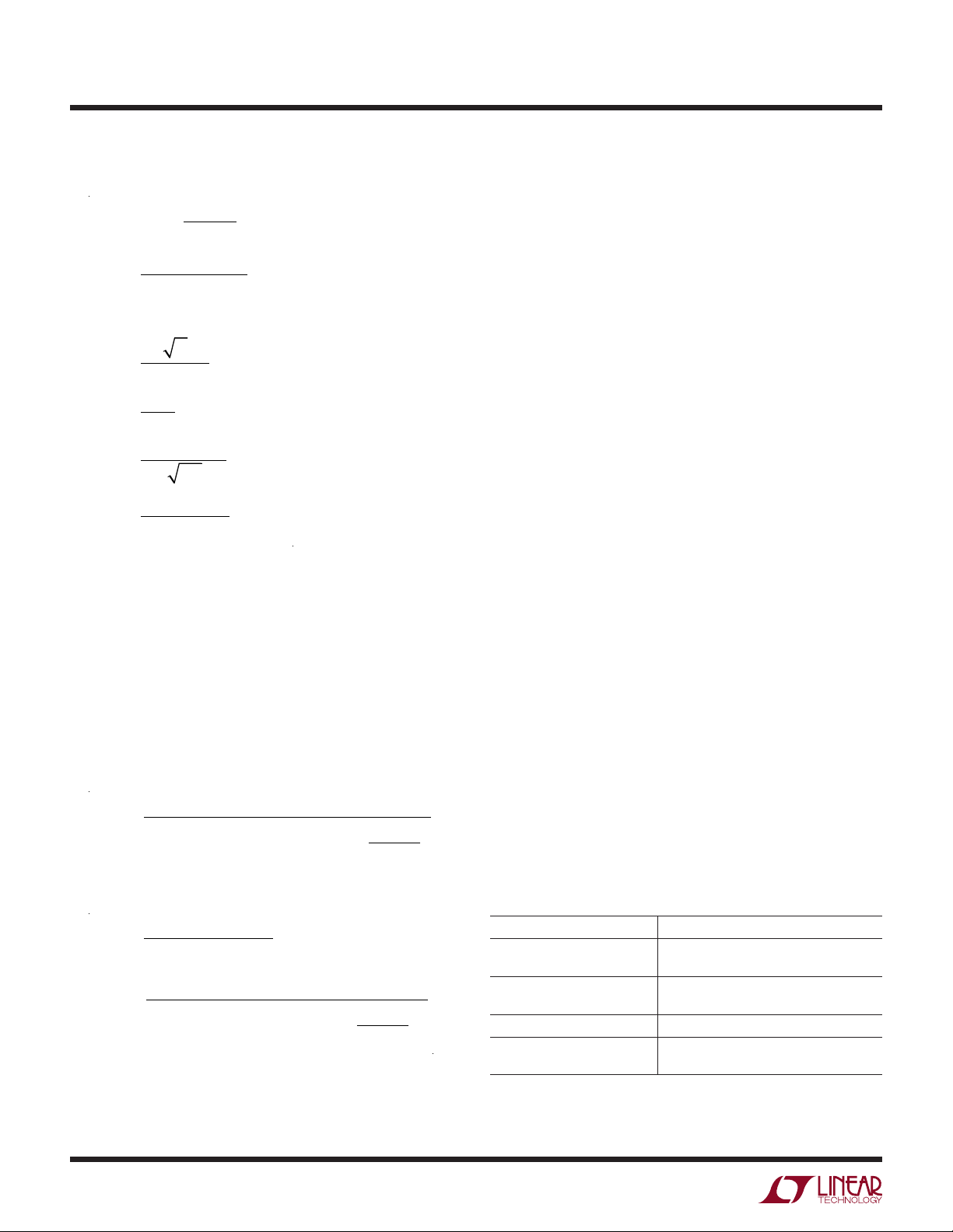
LTC3810-5
applicaTions inForMaTion
TYPE 3 Loop:
BOOST
K = tan
2
C2=
2π • f • G • R
C1=C2 K −1
R2=
( )
K
4
1
FB1
+ 45°
2π • f • C1
R
R3=
FB1
K − 1
C3=
R
=
FB2
1
2πf K •
V
REF(RFB1
− V
V
OUT
R3
)
REF
SPICE or mathematical software can be used to generate
the gain/phase plots for the compensated power supply to
do a sanity check on the component values before trying
them out on the actual hardware. For software, use the
following transfer function:
T(s) = A(s)H(s)
where H(s) was given in Equation 2 and A(s) depends on
compensation circuit used:
Type 2:
1+ s • R2 • C1
• C1+C2
( )
• 1+ s • R2 •
C1• C2
C1+C2
A (s)=
s • R
FB1
Type 3:
1
• C1+C2
( )
FB1
+R3
( )
FB1
1+ s • R3 • C3
•
• C3
• 1+ s• R2 • C1
( )
• 1+ s • R2 •
C1• C2
C1+C2
A (s)=
s • R
1+ s • R
( )
( )
For SPICE, replace VSTIM line in the previous PSPICE
code with following code and generate a gain/phase plot
of V(out)/V(outin):
rfb1 outin vfb 52.5k
rfb2 vfb 0 10k
eithx ithx 0 laplace {0.8-v(vfb)} =
{1/(1+s/1000)}
eith ith 0 value={limit(1e6*v(ithx),0,2.4)}
cc1 ith vfb 4p
cc2 ith x1 8p
rc x1 vfb 210k
rf outin x2 11k ;delete this line for Type 2
cf x2 vfb 120p ;delete this line for Type 2
vstim out outin dc=0 ac=1m
Pulse Skip Mode Operation and MODE/SYNC Pin
The MODE/SYNC pin determines whether the bottom
MOSFET remains on when current reverses in the inductor.
Tying this pin above its 0.8V threshold enables pulse skip
mode operation where the bottom MOSFET turns off when
inductor current reverses. The load current at which current
reverses and discontinuous operation begins depends on
the amplitude of the inductor ripple current and will vary
with changes in V
. Tying the MODE/SYNC pin below the
IN
0.8V threshold forces continuous synchronous operation,
allowing current to reverse at light loads and maintaining
high frequency operation. To prevent forcing current back
into the main power supply, potentially boosting the input
supply to a dangerous voltage level, forced continuous
mode of operation is disabled when the TRACK/SS voltage
is below the reference voltage during soft-start or tracking.
During these two periods, the PGOOD signal is forced low.
Table 1
MODE/SYNC PIN
DC Voltage: 0V to 0.75V
DC Voltage: ≥ 0.85V
Feedback Resistors
Ext. Clock 0V to ≥ 2V
CONDITION
Forced Continuous
Current Reversal Enabled
Pulse Skip Mode Operation
No Current Reversal
Regulating a Secondary Winding
Forced Continuous
Current Reversal Enabled
38105fd
26
Page 27

applicaTions inForMaTion
V
IN
+
C
V
IN
TG
LTC3810-5
R4
FCB
R3
SGND
SW
BG
PGND
Figure 14. Secondary Output Loop
IN
1N4148
V
•
T1
1:N
+
•
+
C
1µF
C
OUT2
OUT
V
38105 F14
OUT2
OUT1
LTC3810-5
ambient temperature, conditions that cause the largest
power loss in the converter. Note that it is important to
check for self-consistency between the assumed MOSFET
junction temperature and the resulting value of I
which heats the MOSFET switches.
Caution should be used when setting the current limit based
upon the R
of the MOSFETs. The maximum current
DS(ON)
limit is determined by the minimum MOSFET on-resistance.
Data sheets typically specify nominal and maximum values
for R
is that the minimum R
, but not a minimum. A reasonable assumption
DS(ON)
lies the same percentage
DS(ON)
below the typical value as the maximum lies above it.
Consult the MOSFET manufacturer for further guidelines.
LIMIT
In addition to providing a logic input to force continuous operation, the MODE/SYNC pin provides a mean to
maintain a flyback winding output when the primary is
operating in pulse skip mode. The secondary output V
OUT2
is normally set as shown in Figure 14 by the turns ratio
N of the transformer. However, if the controller goes into
pulse skip mode and halts switching due to a light primary
load current, then V
divider from V
voltage V
forced until V
V
OUT2(MIN)
OUT2
OUT2(MIN)
OUT2
= 0.8V 1+
will droop. An external resistor
OUT2
to the MODE/SYNC pin sets a minimum
below which continuous operation is
has risen above its minimum.
R4
⎛
⎜
⎝
R3
⎞
⎟
⎠
Fault Conditions: Current Limit and Foldback
The maximum inductor current is inherently limited in a
current mode controller by the maximum sense voltage. In
the LTC3810-5, the maximum sense voltage is controlled
by the voltage on the V
pin. With valley current control,
RNG
the maximum sense voltage and the sense resistance
determine the maximum allowed inductor valley current.
The corresponding output current limit is:
V
I
LIMIT
SNS(MAX )
=
R
DS(ON)ρT
1
+
∆I
L
2
The current limit value should be checked to ensure that
I
LIMIT(MIN)
> I
OUT(MAX)
limit generally occurs with the largest V
. The minimum value of current
at the highest
IN
To further limit current in the event of a short-circuit to
ground, the LTC3810-5 includes foldback current limiting.
If the output falls by more than 50%, then the maximum
sense voltage is progressively lowered to about one-tenth
of its full value.
Be aware also that when the fault timeout is enabled for
the external NMOS regulator, an over current limit may
cause the output to fall below the minimum 4.5V UV
threshold. This condition will cause a linear regulator timeout/restart sequence as described in the Linear Regulator
Timeout section if this condition persists.
Soft-Start and Tracking
The LTC3810-5 has the ability to either soft-start by itself
with a capacitor or track the output of another supply.
When the device is configured to soft-start by itself, a
capacitor should be connected to the TRACK/SS pin. The
LTC3810-5 is put in a low quiescent current shutdown
state (I
~240µA) if the SHDN pin voltage is below 1.5V.
Q
The TRACK/SS pin is actively pulled to ground in this
shutdown state. Once the SHDN pin voltage is above
1.5V, the LTC3810-5 is powered up. A soft-start current
of 1.4µA then starts to charge the soft-start capacitor C
SS
.
Note that soft-start is achieved not by limiting the maximum output current of the controller but by controlling
the ramp rate of the output voltage. Current foldback is
disabled during this soft-start phase. During the soft-start
phase, the LTC3810-5 is ramping the reference voltage
until it reaches 0.8V. The force continuous mode is also
38105fd
27
Page 28
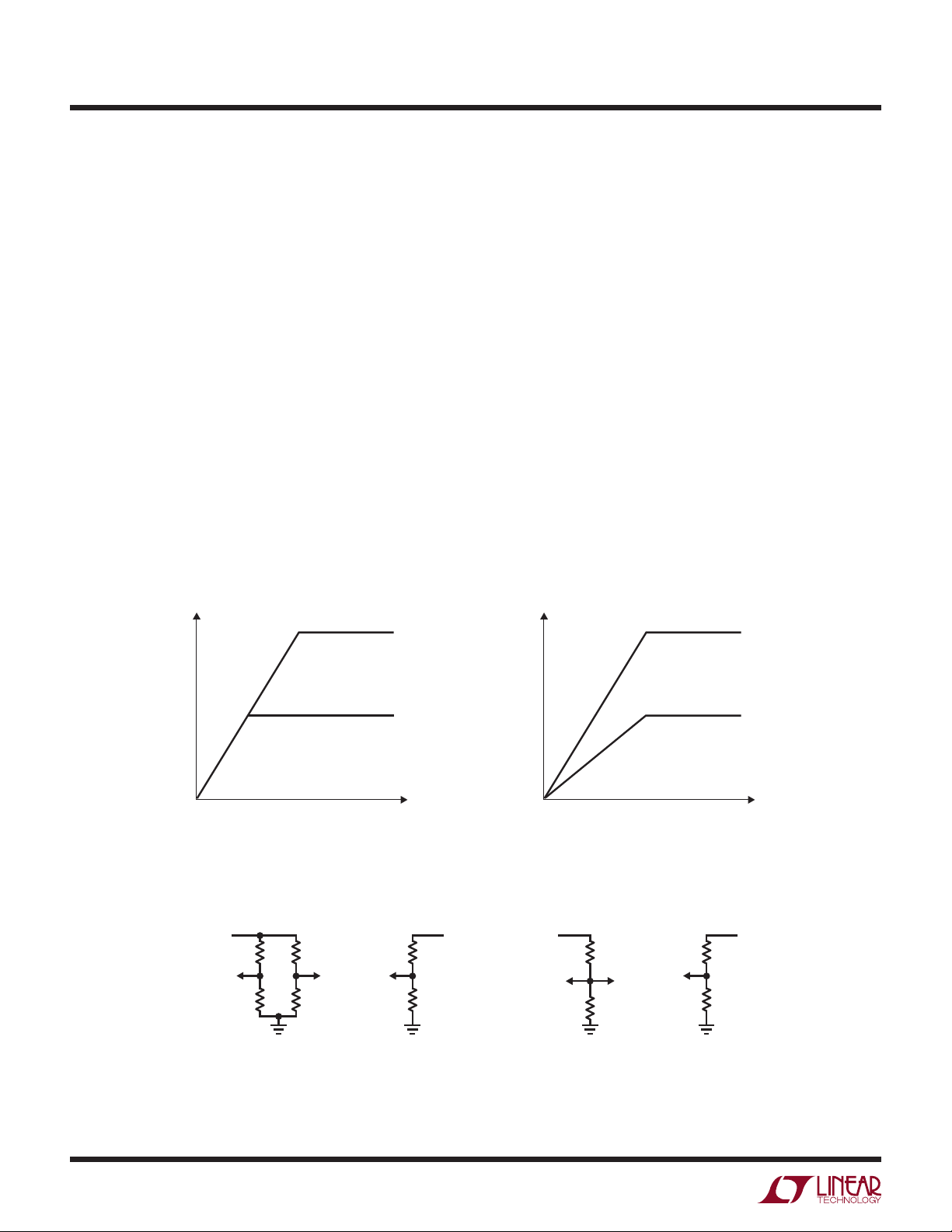
LTC3810-5
applicaTions inForMaTion
disabled and PGOOD signal is forced low during this phase.
The total soft-start time can be calculated as:
t
SOFTSTART
= 0.8 • CSS/1.4µA
When the device is configured to track another supply,
the feedback voltage of the other supply is duplicated
by a resistor divider and applied to the TRACK/SS pin.
Therefore, the voltage ramp rate on this pin is determined
by the ramp rate of the other supply output voltage.
Output Voltage Tracking
The LTC3810-5 allows the user to program how its output ramps up by means of the TRACK/SS pin. Through
this pin, the output can be set up to either coincidentally
or ratiometrically track with another supply’s output, as
shown in Figure 15. In the following discussions, V
refers to the master LTC3810-5’s output and V
OUT2
OUT1
refers
to the slave LTC3810-5’s output.
To implement the coincident tracking in Figure 15a, connect an additional resistive divider to V
and connect its
OUT1
midpoint to the TRACK/SS pin of the slave IC. The ratio of
this divider should be selected the same as that of the slave
IC’s feedback divider shown in Figure 16. In this tracking
mode, V
must be set higher than V
OUT1
. To implement
OUT2
the ratiometric tracking, the ratio of the divider should be
exactly the same as the master IC’s feedback divider. Note
that the internal soft-start current will introduce a small
error on the tracking voltage depending on the absolute
values of the tracking resistive divider.
By selecting different resistors, the LTC3810-5 can achieve
different modes of tracking including the two in Figure 15.
So which mode should be programmed? While either
mode in Figure 15 satisfies most practical applications,
there do exist some tradeoffs. The ratiometric mode saves
a pair of resistors, but the coincident mode offers better
output regulation. This can be better understood with the
OUTPUT VOLTAGE
(15a) Coincident Tracking
V
OUT1
TRACK/SS2
PIN
R3 R1
TO
R4 R2
(16a) Coincident Tracking Setup
V
OUT1
V
OUT2
OUTPUT VOLTAGE
TIME
(15b) Ratiometric Tracking
Figure 15. Two Different Modes of Output Voltage Tracking
V
OUT1
TO
TRACK/SS2
PIN
R1
R2
(16b) Ratiometric Tracking Setup
TO
V
PIN
FB1
V
OUT2
R3
TO
V
FB2
PIN
R4
TO
V
PIN
FB1
TIME
V
OUT1
V
OUT2
38105 F15
V
OUT2
R3
TO
V
FB2
PIN
R4
38105 F16
28
Figure 16. Setup for Coincident and Ratiometric Tracking
38105fd
Page 29
applicaTions inForMaTion
I I
+
D2
FB2
EA2
–
D3
38105 F17
and the internal
FB2
slightly lower than 0.8V.
0.8V
V
FB2
D1
TRACK/SS2
Figure 17. Equivalent Input Circuit of Error Amplifier
help of Figure 17. At the input stage of the slave IC’s error
amplifier, two common anode diodes are used to clamp
the equivalent reference voltage and an additional diode
is used to match the shifted common mode voltage. The
top two current sources are of the same amplitude. In the
coincident mode, the TRACK/SS voltage is substantially
higher than 0.8V at steady state and effectively turns off
D1. D2 and D3 will therefore conduct the same current
and offer tight matching between V
precision 0.8V reference. In the ratiometric mode, however,
TRACK/SS equals 0.8V at steady state. D1 will divert part
of the bias current to make V
Although this error is minimized by the exponential I-V
characteristic of the diode, it does impose a finite amount
of output voltage deviation. Furthermore, when the master
IC’s output experiences dynamic excursion (under load
transient, for example), the slave IC output will be affected
as well. For better output regulation, use the coincident
tracking mode instead of ratiometric.
LTC3810-5
The internal oscillator locks to the external clock after
the second clock transition is received. When external
synchronization is detected, LTC3810-5 will operate in
forced continuous mode. If an external clock transition
is not detected for three successive periods, the internal
oscillator will revert to the frequency programmed by the
resistor.
R
ON
During the start-up phase, phase-locked loop function is
disabled. When LTC3810-5 is not in synchronization mode,
PLL/LPF pin voltage is set to around 1.215V. Frequency
synchronization is accomplished by changing the internal
on-time current according to the voltage on the PLL/LPF pin.
The phase detector used is an edge sensitive digital type
which provides zero degrees phase shift between the external and internal pulses. This type of phase detector will
not lock up on input frequencies close to the harmonics
of the V
is equal to the capture range, Df
DfH = DfC = ±0.3 f
The output of the phase detector is a complementary pair of
current sources charging or discharging the external filter
network on the PLL
is shown in Figure 18.
center frequency. The PLL hold-in range, DfH,
CO
C:
O
/LPF
pin. A simplified block diagram
R
LP
2.4V
PLL/LPF
C
LP
Phase-Locked Loop and Frequency Synchronization
The LTC3810-5 has a phase-locked loop comprised of an
internal voltage controlled oscillator and phase detector.
This allows the top MOSFET turn-on to be locked to the
rising edge of an external source. The frequency range
of the voltage controlled oscillator is ±30% around the
center frequency f
. The center frequency is the operating
O
frequency discussed in the Operating Frequency section.
The LTC3810-5 incorporates a pulse detection circuit that
will detect a clock on the MODE/SYNC pin. In turn, it will
turn on the phase-locked loop function. The pulse width of
the clock has to be greater than 400ns and the amplitude
of the clock should be greater than 2V.
MODE/SYNC
DIGITAL
PHASE/
FREQUENCY
DETECTOR
Figure 18. Phase-Locked Loop Block Diagram
VCO
38105 F18
38105fd
29
Page 30

LTC3810-5
applicaTions inForMaTion
If the external frequency (f
oscillator frequency f
pulling up the PLL
is less than f
the PLL
, current is sunk continuously, pulling down
O
/LPF
pin. If the external and internal frequencies
, current is sourced continuously,
O
/LPF
pin. When the external frequency
) is greater than the
MODE
are the same but exhibit a phase difference, the current
sources turn on for an amount of time corresponding to
the phase difference. Thus the voltage on the PLL/LPF
pin is adjusted until the phase and frequency of the external
and internal oscillators are identical. At this stable operating
point the phase comparator output is open and the filter
capacitor C
holds the voltage. The LTC3810-5 MODE/
LP
SYNC pin must be driven from a low impedance source
such as a logic gate located close to the pin.
The loop filter components (C
, RLP) smooth out the
LP
current pulses from the phase detector and provide a
stable input to the voltage controlled oscillator. The filter
components C
acquires lock. Typically R
and RLP determine how fast the loop
LP
= 10kΩ and CLP is 0.01µF
LP
to 0.1µF.
Efficiency Considerations
The percent efficiency of a switching regulator is equal to
the output power divided by the input power times 100%.
It is often useful to analyze individual losses to determine
what is limiting the efficiency and which change would
produce the most improvement. Although all dissipative
elements in the circuit produce losses, four main sources
account for most of the losses in LTC3810-5 circuits:
2
1. DC I
R losses. These arise from the resistances of the
MOSFETs, inductor and PC board traces and cause the
efficiency to drop at high output currents. In continuous
mode the average output current flows through L, but is
chopped between the top and bottom MOSFETs. If the
two MOSFETs have approximately the same R
DS(ON)
,
then the resistance of one MOSFET can simply be
summed with the resistances of L and the board traces
to obtain the DC I
0.01Ω and R
= 0.005Ω, the loss will range from 15mW
L
R loss. For example, if R
DS(ON)
=
2
to 1.5W as the output current varies from 1A to 10A.
2. Transition loss. This loss arises from the brief amount
of time the top MOSFET spends in the saturated region
during switch node transitions. It depends upon the
input voltage, load current, driver strength and MOSFET
capacitance, among other factors. The loss is significant at input voltages above 20V and can be estimated
from the second term of the P
equation found in
MAIN
the Power MOSFET Selection section. When transition
losses are significant, efficiency can be improved by
lowering the frequency and/or using a top MOSFET(s)
with lower C
3. INTV
CC
at the expense of higher R
RSS
/DRVCC current. This is the sum of the MOSFET
DS(ON)
.
driver and control currents. Control current is typically
about 3mA and driver current can be calculated by:
I
GATE
= f(Q
G(TOP)
+ Q
G(BOT)
), where Q
G(TOP)
and Q
G(BOT)
are the gate charges of the top and bottom MOSFETs.
This loss is proportional to the supply voltage that
INTV
NMOS linear regulator, V
regulator, or V
to INTV
4. C
/DRVCC is derived from, i.e., VIN for the external
CC
for the internal EXTVCC
OUT
when an external supply is connected
EXT
/DRVCC.
CC
loss. The input capacitor has the difficult job of fil-
IN
tering the large RMS input current to the regulator. It
have a very low ESR to minimize the AC I2R loss
must
and sufficient capacitance to prevent the RMS current
causing additional upstream losses in fuses or
from
batteries.
Other losses, including C
ESR loss, Schottky diode D1
OUT
conduction loss during dead time and inductor core loss
generally account for less than 2% additional loss. When
making adjustments to improve efficiency, the input current is the best indicator of changes in efficiency. If you
make a change and the input current decreases, then the
efficiency has increased. If there is no change in input
current, then there is no change in efficiency.
Checking Transient Response
The regulator loop response can be checked by looking at the load transient response. Switching regulators
take several cycles to respond to a step in load current.
30
38105fd
Page 31

( )
applicaTions inForMaTion
LTC3810-5
When load step occurs, V
amount equal to DI
series resistance of C
discharge C
generating a feedback error signal used by
OUT
the regulator to return V
this recovery time, V
(ESR), where ESR is the effective
LOAD
OUT
OUT
OUT
immediately shifts by an
OUT
. DI
also begins to charge or
LOAD
to its steady-state value. During
can be monitored for overshoot
or ringing that would indicate a stability problem.
Design Example
As a design example, take a supply with the following
specifications: V
= 12V to 60V, V
IN
= 5V ±5%, I
OUT
OUT(MAX)
= 6A, f = 250kHz. First, calculate the timing resistor:
5V
=110k
RON=
2.4V • 250kHz • 76pF
and choose the inductor for about 40% ripple current at
5V
IN
:
5V
⎛
1−
⎜
⎝
60V
⎞
= 7.6µH
⎟
⎠
the maximum V
L =
250kHz • 0.4 • 6A
V
= 320mV, assume a junction temperature of about
SNS
55°C above a 70°C ambient (ρ
I
LIMIT
320mV
≥
1.7 • 0.031Ω
1
+
• 2.4A =7.3A
2
125°C
= 1.7):
and double-check the assumed TJ in the MOSFET:
BOT
60V −5V
=
60V
• 7.3A2• 1.7 • 0.031Ω= 2.6W
P
TJ = 70°C + 2.6W • 22°C/W = 127°C
Verify that the Si7850DP is also a good choice for the
top MOSFET by checking its power dissipation at current
limit and maximum input voltage, assuming a junction
temperature of 30°C above a 70°C ambient (ρ
P
MAIN
+ 60V2•
= 0.206W +1.32W =1.53W
5V
=
• 7.3A21.5 • 0.031Ω
60V
7.3A
• 2Ω• 183pF •
2
1
⎛
⎜
⎝
5V −3.8V
+
3.8V
100°C
1
= 1.5):
⎞
• 250kHz
⎟
⎠
With a 7.7µH inductor, ripple current will vary from 1.5A
to 2.4A (25% to 40%) over the input supply range.
Next, choose the bottom MOSFET switch. Since the
drain of the MOSFET will see the full supply voltage 60V
(max) plus any ringing, choose an 60V MOSFET. The
Si7850DP has:
BV
R
δ
C
V
θ
= 60V
DSS
= 31mΩ (max)/25mΩ (nom),
DS(ON)
= 0.007/°C,
= (8.3nC – 2.8nC)/30V = 183pF,
MILLER
GS(MILLER)
= 22°C/W.
JA
= 3.8V,
This yields a nominal sense voltage of:
V
SNS(NOM)
= 6A • 1.3 • 0.025Ω = 195mV
To guarantee proper current limit at worst-case conditions,
increase nominal V
to 2V). To check if the current limit is acceptable at
V
RNG
by at least 50% to 320mV (by tying
SNS
TJ = 70°C + 1.53W • 22°C/W = 104°C
The junction temperature will be significantly less at nominal current, but this analysis shows that careful attention to
heat sinking on the board will be necessary in this circuit.
Since V
from V
the EXTV
> 4.7V, the INTVCC voltage can be generated
OUT
with the internal LDO by connecting V
OUT
pin. A small SOT23 MOSFET such as the
CC
OUT
to
ZXMN10A07F can be used for the pass device if fault
timeout is enabled. Choose R
to guarantee that fault
NDRV
timeout is enabled when power dissipation of M3 exceeds
0.4W (max for 70°C ambient):
= 250kHz • 2 • 18nC + 3mA = 12mA
I
CC
R
NDRV
So, choose R
0.4W / 0.012A – 3V
≤
270µA
= 100k.
NDRV
=112k
38105fd
31
Page 32

LTC3810-5
applicaTions inForMaTion
CIN is chosen for an RMS current rating of about 3A at
85°C. The output capacitors are chosen for a low ESR
of 0.018Ω to minimize output voltage changes due to
inductor ripple current and load steps. The ripple voltage
will be only:
DV
OUT(RIPPLE)
= DI
• ESR = 2.4A • 0.018W
L(MAX)
= 43mV
However, a 0A to 6A load step will cause an output change
of up to:
DV
OUT(STEP)
= DI
• ESR = 6A • 0.018Ω
LOAD
= 108mV
An optional 10µF ceramic output capacitor is included
to minimize the effect of ESL in the output ripple. The
complete circuit is shown in Figure 19.
R
ON
110k
C
ON
PGOOD
250kHz
CLOCK
SHDN
R
UV1
200k
R
UV2
14.3k
0.01µF
R
FB2
1.91k
10k
78.7k
C
SS
1000pF
R
200k
10k
C
47pF
C
100pF
C2
C
C1
5pF
31
I
ON
2
V
ON
3
V
RNG
4
PGOOD
5
MODE_SYNC
6
I
TH
7
V
FB
8
PLL/LPF
9
SS/TRACK
33
SGND
12
SHDN
13
U
VIN
LTC3810-5
SGND PGND
R
SENSE
FB1
10k
BOOST
SENSE
BGRTN
DRV
INTV
EXTV
NDRV
TG
SW
BG
27
26
25
24
+
20
–
19
18
17
CC
16
CC
15
CC
14
PC Board Layout Checklist
When laying out a PC board follow one of two suggested
approaches. The simple PC board layout requires a dedicated ground plane layer. Also, for higher currents, it is
recommended to use a multilayer board to help with heat
sinking power components.
• The ground plane layer should not have any traces and
it should be as close as possible to the layer with power
MOSFETs.
• Place C
IN
, C
, MOSFETs, D1 and inductor all in one
OUT
compact area. It may help to have some components
on the bottom side of the board.
•
Use an immediate via to connect the components to
ground plane including SGND and PGND of LTC3810-5.
Use several bigger vias for power components.
V
IN
R
NDRV
100k
CB 0.1µF
C
DRVCC
0.1µF
C
VCC
1µF
DB
BAS19
M3
ZXMN10A07F
C5
1µF
M1
SiR880DP
M2
SiR880DP
C
IN1
68µF
100V
10µH
D1
B1100
12V TO 60V
C
IN2
1µF
100V
PGND
L1
C
270µF
6.3V
38105 F19
OUT1
V
5V
6A
C
OUT2
10µF
6.3V
OUT
32
Figure 19. 12V to 60V Input Voltage to 5V/6A Synchronized at 250kHz
38105fd
Page 33

applicaTions inForMaTion
LTC3810-5
• Use compact plane for switch node (SW) to improve
cooling of the MOSFETs and to keep EMI down.
• Use planes for V
and V
IN
to maintain good voltage
OUT
filtering and to keep power losses low.
• Flood all unused areas on all layers with copper. Flooding
with copper will reduce the temperature rise of power
component. You can connect the copper areas to any
DC net (V
IN
, V
, GND or to any other DC rail in your
OUT
system).
When laying out a printed circuit board, without a ground
plane, use the following checklist to ensure proper operation of the controller.
• Segregate the signal and power grounds. All small
signal components should return to the SGND pin at
one point which is then tied to the PGND pin close to
the source of M2.
• Place M2 as close to the controller as possible, keeping
the PGND, BG and SW traces short.
•
Connect the input capacitor(s) CIN close to the power MOSFETs. This capacitor carries the MOSFET AC
current.
• Keep the high dV/dt SW, BOOST and TG nodes away
from sensitive small-signal nodes.
• Connect the INTV
to the INTV
CC
• Connect the top driver boost capacitor C
decoupling capacitor C
CC
and SGND pins.
closely
VCC
closely to
B
the BOOST and SW pins.
• Connect the bottom driver decoupling capacitor C
closely to the DRV
and BGRTN pins.
CC
DRVCC
38105fd
33
Page 34
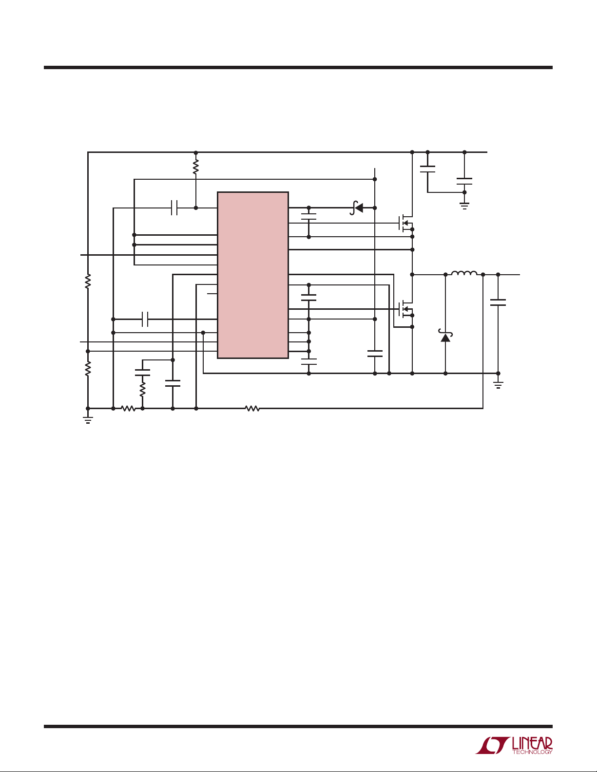
LTC3810-5
Typical applicaTions
7V to 60V Input Voltage to 5V/5A with IC Power from 12V Supply
R
110k
C
ON
100pF
PGOOD
R
UV1
470k
C
SS
1000pF
SHDN
R
UV2
61.9k
R
1.91k
FB2
C
47pF
R
C
100k
C2
C
C1
5pF
ON
31
2
3
4
5
6
7
8
9
33
12
13
and All Ceramic Output Capacitors
12V
DB
DRVCC
VCC
BAS19
C5
22µF
M2
Si7850DP
LTC3810-5
I
ON
V
ON
V
RNG
PGOOD
MODE_SYNC
I
TH
V
FB
PLL/LPF
SS/TRACK
SGND
SHDN
UVIN
SGND PGND
R
FB1
10k
BOOST
SENSE
SENSE
BGRTN
DRV
INTV
EXTV
NDRV
TG
SW
BG
27
CB 0.1µF
26
25
24
+
20
–
19
C
0.1µF
18
17
CC
16
CC
15
CC
14
C
1µF
M1
Si7850DP
C
IN1
68µF
100V
L1
4.7µH
D1
B1100
38105 TA03
C
IN2
1µF
100V
PGND
V
IN
7V TO 60V
C
OUT
47µF
6.3V
×3
V
OUT
5V
5A
34
38105fd
Page 35
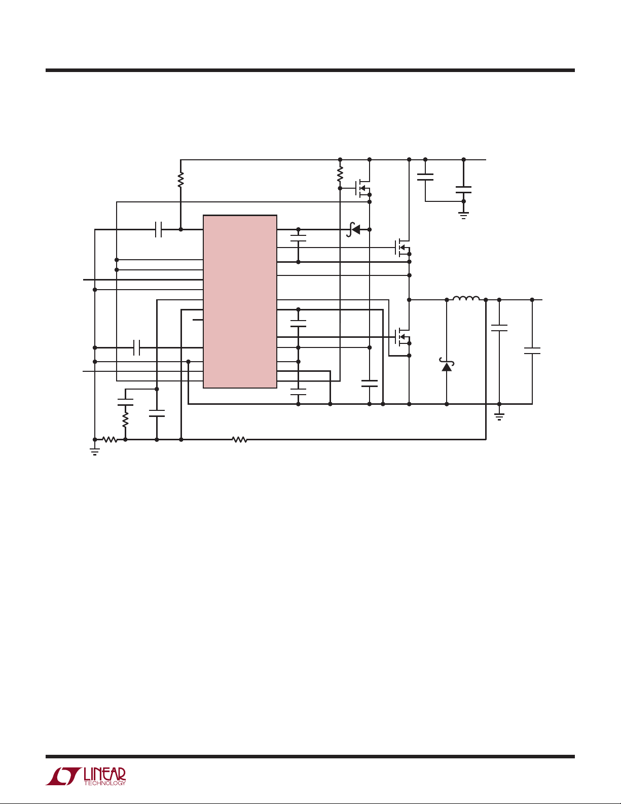
Typical applicaTions
15V to 60V Input Voltage to 3.3V/5A with Fault Timeout,
R
ON
71.5k
C
ON
PGOOD
SHDN
R
FB2
3.24k
C
SS
1000pF
C
C2
47pF
R
C
200k
100pF
C
5pF
31
I
ON
2
V
3
V
4
PGOOD
5
MODE_SYNC
6
I
TH
7
V
8
PLL/LPF
9
SS/TRACK
33
SGND
12
SHDN
13
UVIN
C1
Pulse Skip and VIN UV Disabled
R
NDRV
215k
LTC3810-5
ON
RNG
FB
SGND PGND
R
FB1
10.2k
BOOST
SENSE
SENSE
BGRTN
DRV
INTV
EXTV
NDRV
TG
SW
BG
27
C
B
0.1µF
26
25
24
+
20
–
19
C
DRVCC
0.1µF
18
17
CC
16
CC
15
CC
14
C
VCC
1µF
DB
BAS19
C5
1µF
M3
ZVN4210G
M1
Si7850DP
M2
Si7850DP
C
IN1
68µF
100V
LTC3810-5
V
IN
15V TO 60V
C
IN2
1µF
100V
PGND
L1
4.7µH
C
270µF
6.3V
D1
B1100
38105 TA04
OUT1
V
3.3V
5A
C
OUT2
10µF
6.3V
OUT
38105fd
35
Page 36

LTC3810-5
package DescripTion
5.50 ±0.05
4.10 ±0.05
3.50 REF
(4 SIDES)
APPLY SOLDER MASK TO AREAS THAT ARE NOT SOLDERED
3.45 ± 0.05
3.45 ± 0.05
RECOMMENDED SOLDER PAD LAYOUT
5.00 ± 0.10
(4 SIDES)
PIN 1
TOP MARK
(NOTE 6)
UH Package
32-Lead Plastic QFN (5mm × 5mm)
(Reference LTC DWG # 05-08-1693 Rev D)
0.70 ±0.05
PACKAGE OUTLINE
0.25 ± 0.05
0.50 BSC
0.75 ± 0.05
R = 0.05
0.00 – 0.05
TYP
BOTTOM VIEW—EXPOSED PAD
R = 0.115
TYP
31
PIN 1 NOTCH R = 0.30 TYP
OR 0.35 × 45° CHAMFER
32
0.40 ± 0.10
1
2
3.50 REF
(4-SIDES)
0.200 REF
NOTE:
1. DRAWING PROPOSED TO BE A JEDEC PACKAGE OUTLINE
M0-220 VARIATION WHHD-(X) (TO BE APPROVED)
2. DRAWING NOT TO SCALE
3. ALL DIMENSIONS ARE IN MILLIMETERS
4. DIMENSIONS OF EXPOSED PAD ON BOTTOM OF PACKAGE DO NOT INCLUDE
MOLD FLASH. MOLD FLASH, IF PRESENT, SHALL NOT EXCEED 0.20mm ON ANY SIDE
5. EXPOSED PAD SHALL BE SOLDER PLATED
6. SHADED AREA IS ONLY A REFERENCE FOR PIN 1 LOCATION
ON THE TOP AND BOTTOM OF PACKAGE
3.45 ± 0.10
3.45 ± 0.10
(UH32) QFN 0406 REV D
0.25 ± 0.05
0.50 BSC
36
38105fd
Page 37
LTC3810-5
revision hisTory
REV DATE DESCRIPTION PAGE NUMBER
D 12/10 Change to Operating Temperature Range
Updated Order Information table
Change made to Feedback Voltage (V
Change to Note 2 and Note 7
Addition of 150°C to graphs G14, G17, G18, G19, G20, G23, G24, G25, G28 and G30
Formula change: Type 2 and Type 3
Updated Related Parts table
(Revision history begins at Rev D)
)
FB
2
2
3
4
6, 7, 8
26
38
Information furnished by Linear Technology Corporation is believed to be accurate and reliable.
However, no responsibility is assumed for its use. Linear Technology Corporation makes no representation that the interconnection of its circuits as described herein will not infringe on existing patent rights.
38105fd
37
Page 38
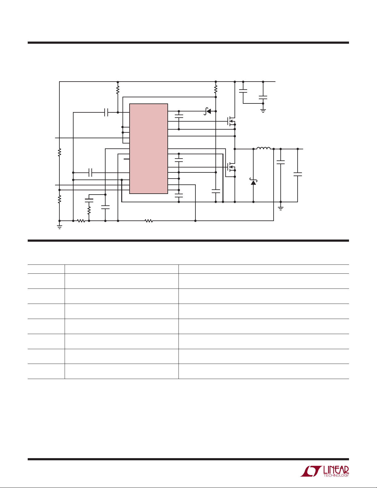
LTC3810-5
Typical applicaTion
13V to 60V Input Voltage to 12V/10A with Trickle Charger Start-Up
R
263k
C
ON
100pF
PGOOD
R
UV1
200k
C
SS
1000pF
SHDN
R
UV2
13.3k
C
C2
47pF
C
R
C
R
FB2
200k
1k
5pF
C1
ON
31
2
3
4
5
6
7
8
9
33
12
13
R
NDRV
100k
DB
C
B
0.1µF
C
DRVCC
0.1µF
C
VCC
1µF
BAS19
C5
22µF
LTC3810-5
I
ON
V
ON
V
RNG
PGOOD
MODE_SYNC
I
TH
V
FB
PLL/LPF
SS/TRACK
SGND
SHDN
UVIN
SGND PGND
R
FB1
14k
BOOST
SENSE
SENSE
BGRTN
DRV
INTV
EXTV
NDRV
SW
27
26
TG
25
24
+
20
–
19
18
BG
17
CC
16
CC
15
CC
14
M1
Si7850DP
M2
Si7850DP
×2
C
IN1
68µF
100V
L1
10µH
D1
B1100
C
1µF
100V
PGND
V
13V TO 60V
IN2
38105 TA05
IN
V
OUT
12V
10A
C
OUT1
270µF
16V
C
OUT2
10µF
16V
relaTeD parTs
PART NUMBER DESCRIPTION COMMENTS
LTC3891 60V, Low I
, Synchronous Step-Down DC/DC
Q
Controller
LTC3890 60V, Low I
, Dual Output 2-Phase Synchronous
Q
Step-Down DC/DC Controller
LTC3810 100V Synchronous Step-Down DC/DC Controller Constant On-time Valley Current Mode, 4V ≤ V
LTC3812-5 60V Synchronous Step-Down DC/DC Controller Constant On-time Valley Current Mode, 4V ≤ V
LTC3703 100V Synchronous Step-Down DC/DC Controller PLL Fixed Frequency 100kHz to 600kHz, 4V ≤ V
LT3845A 60V, Low I
, Single Output Synchronous Step-Down
Q
DC/DC Controller
LTC3824 60V, Low I
, Step-Down DC/DC Controller, 100%
Q
Duty Cycle
PLL Fixed Frequency 50kHz to 900kHz, 4V ≤ VIN ≤ 60V, 0.8V ≤ V
TSSOP-20E, 3mm × 4mm QFN-20
PLL Fixed Frequency 50kHz to 900kHz, 4V ≤ VIN ≤ 60V, 0.8V ≤ V
5mm × 5mm QFN-32
SSOP-28
IN
TSSOP-16E
IN
SSOP-16, SSOP-28
IN
Adjustable Fixed Frequency 100kHz to 500kHz, 4V≤ VIN ≤ 60V, 1.23V ≤ V
36V, TSSOP-16E
Selectable Fixed Frequency 200kHz to 600kHz, 4V≤ VIN ≤ 60V, 0.8V ≤ V
I
= 40µA, MSOP-10E
Q
≤ 60V, 0.8V ≤ V
≤ 60V, 0.8V ≤ V
≤ 100V, 0.8V ≤ V
≤ 24V,
OUT
≤ 24V,
OUT
≤ 0.93VIN,
OUT
≤ 0.93VIN,
OUT
≤ 0.93VIN,
OUT
OUT
OUT
≤ VIN,
≤
38
Linear Technology Corporation
1630 McCarthy Blvd., Milpitas, CA 95035-7417
(408) 432-1900 l FAX: (408) 434-0507
l
www.linear.com
38105fd
LT 1210 REV D • PRINTED IN USA
LINEAR TECHNOLOGY CORPORATION 2007
 Loading...