

Page 1
LTC3545/LTC3545-1
1
35451fa
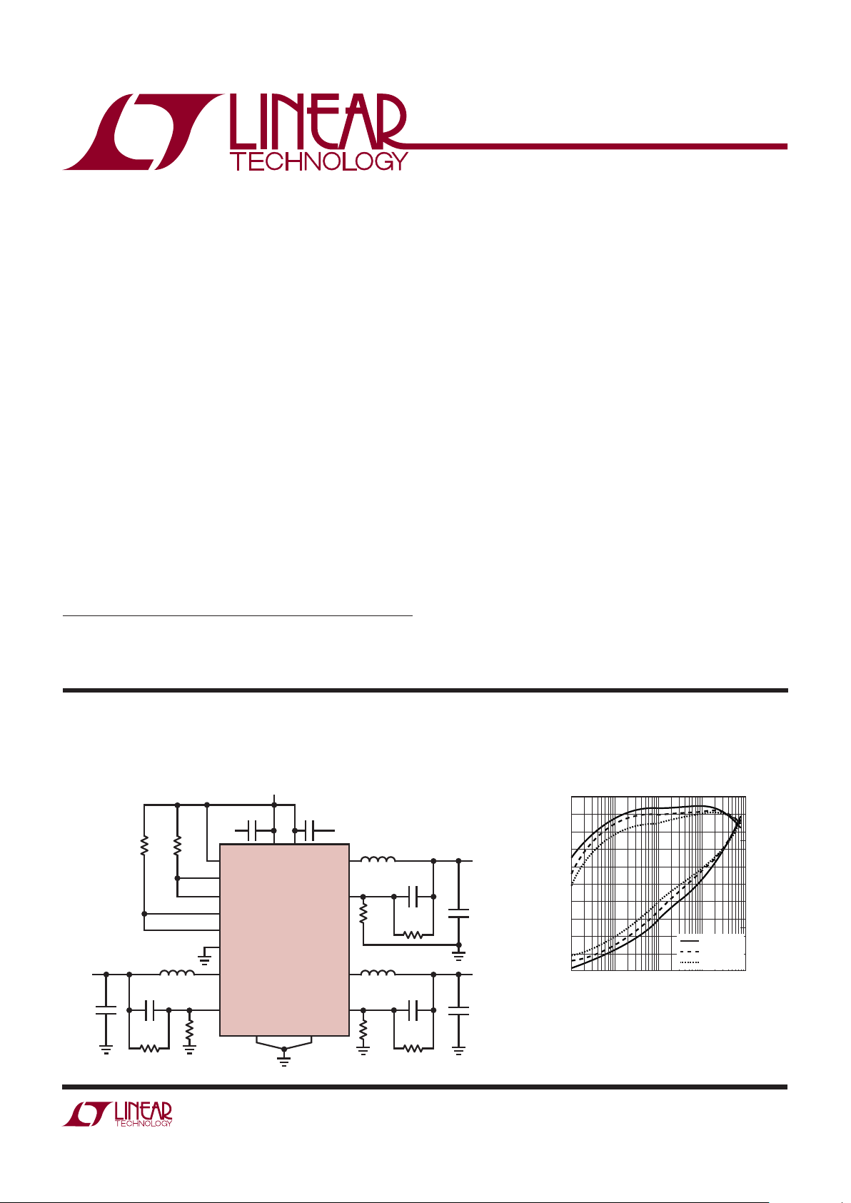
TYPICAL APPLICATION
FEATURES
APPLICATIONS
DESCRIPTION
Triple 800mA Synchronous
Step-Down Regulator–2.25MHz
The LTC®3545/LTC3545-1 are triple, high efficiency,
monolithic synchronous buck regulators using a constant
frequency, current mode architecture. The regulators operate independently with separate run pins. The 2.25V to
5.5V input voltage range makes the LTC3545/LTC3545-1
well suited for single Li-Ion battery-powered applications.
Low ripple pulse skip mode or high effi ciency Burst Mode
operation is externally selectable. PWM pulse skip mode
operation provides very low output ripple voltage while
Burst Mode operation increases effi ciency at low output
loads.
Switching frequency is internally set to 2.25MHz, or the
switching frequency can be synchronized to an external
1MHz to 3MHz clock. Power good indicators easily allow
power on sequencing between the three regulators.
The internal synchronous switches increase effi ciency and
eliminate external Schottky diodes. Low output voltages are
supported with the 0.6V feedback reference voltage.
The LTC3545-1 replaces the SYNC/MODE function with a
third PGOOD pin and forces Burst Mode operation.
■
Three 800mA Outputs
■
High Effi ciency: Up to 95%
■
2.25V to 5.5V Input Voltage Range
■
Low Ripple (<20mV
P-P
) Burst Mode® Operation
I
Q
: 58μA
■
2.25MHz Constant Frequency Operation or
■
Synchronizable to External 1MHz to 3MHz Clock
■
Power Good Indicators Ease Supply Sequencing
■
0.6V Reference Allows Low Output Voltages
■
Current Mode Operation/Excellent Transient Response
■
Low Profi le 16-Lead 3mm × 3mm QFN Package
■
Smart Phones
■
Wireless and DSL Modems
■
Digital Still Cameras
■
Portable Instruments
■
Point of Load Regulation
High Effi ciency Triple Step-Down Converter with Power Sequencing
Effi ciency and Loss vs Load Current
L, LT, LTC, LTM and Burst Mode are registered trademarks of Linear Technology Corporation.
All other trademarks are the property of their respective owners.
Protected by U.S. Patents including 6580258, 5481178, 6127815, 6498466, 6611131.
3545 TA01
L1
1.5µH
C5
10µF
PGNDGNDA
C4 10µF
C6
20pF
R2
255k
R1
511k
C1
10µF
V
OUT1
1.8V
V
IN
2.25V TO 5.5V
RUN1
PGOOD1
RUN2
PGOOD2
RUN3
L2
1.5µH
R4
226k
C2
10µF
V
OUT2
1.2V
SW2
V
FB2
SYNC/MODE
SW1
V
FB1
VINPV
IN
LTC3545
GNDA PGND
R7
500k
C7
20pF
R3
226k
R8
500k
L3
1.5µH
R6
200k
C3
10µF
V
OUT3
1.5V
SW3
V
FB3
C8
20pF
R5
301k
LOAD CURRENT (A)
30
EFFICIENCY (%)
LOSS (W)
90
100
20
10
80
50
70
60
40
0.0001 0.01 0.1 1
3545 TA01b
0
0.001
1
0.1
0.01
0.0001
0.001
VIN = 2.5V
V
IN
= 3.6V
V
IN
= 4.2V
TA = 25°C
V
OUT
= 2V
Burst Mode OPERATION
f
OSC
= 2.25MHz
SINGLE CHANNEL
Page 2
LTC3545/LTC3545-1
2
35451fa
ELECTRICAL CHARACTERISTICS
ABSOLUTE MAXIMUM RATINGS
Input Supply Voltage .................................... –0.3V to 6V
RUNx, PGOODx ..............................–0.3V to (V
IN
+ 0.3V)
V
FBx
, SYNC/MODE .........................–0.3V to (VIN + 0.3V)
SWx ...............................................–0.3V to (V
IN
+ 0.3V)
P-Switch Source Current (DC) (Note 8) ...................1.1A
(Note 1)
SYMBOL PARAMETER CONDITIONS MIN TYP MAX UNITS
General Characteristics
V
IN
Input Voltage Range
●
2.25 5.5 V
V
FBx
Regulated Feedback Voltage (Note 5) TA = 25°C,
0°C ≤ T
A
≤ 85°C
●
0.592
0.588
0.6
0.6
0.608
0.612
V
V
ΔV
FBx
Reference Voltage Line Regulation (Note 5) VIN = 2.25V to 5.5V
●
0.08 0.15 %/V
V
LOADREG
Output Voltage Load Regulation (Note 6) 0.5 %
The ● denotes the specifi cations which apply over the full operating
temperature range, otherwise specifi cations are at TA = 25°C. VIN = 3.6V unless otherwise noted. (Note 2)
N-Channel Sink Current (DC) (Note 8) .....................1.1A
Peak SW Sink and Source Current (Note 8) .............1.3A
Operating Temperature Range.................. –40°C to 85°C
Junction Temperature (Notes 3, 4)........................ 125°C
Storage Temperature Range ...................–65°C to 125°C
16 15 14 13
5 6 7 8
17
UD PACKAGE
16-LEAD (3mm s 3mm) PLASTIC QFN
TOP VIEW
9
10
11
12
4
3
2
1SW1
PGOOD1
RUN2
PGOOD2
V
FB2
V
FB3
RUN3
SYNC/MODE
GNDA
VINRUN1
V
FB1
SW2
PGND
PV
IN
SW3
T
JMAX
= 125°C, θJA = 68°C/W
EXPOSED PAD (PIN 17) IS GND, MUST BE SOLDERED TO PCB
16 15 14 13
5 6 7 8
TOP VIEW
17
UD PACKAGE
16-LEAD (3mm s 3mm) PLASTIC QFN
9
10
11
12
4
3
2
1SW1
PGOOD1
RUN2
PGOOD2
V
FB2
V
FB3
RUN3
PGOOD3
GNDA
VINRUN1
V
FB1
SW2
PGND
PV
IN
SW3
T
JMAX
= 125°C, θJA = 68°C/W
EXPOSED PAD (PIN 17) IS GND, MUST BE SOLDERED TO PCB
PIN CONFIGURATION
LEAD FREE FINISH TAPE AND REEL PART MARKING PACKAGE DESCRIPTION TEMPERATURE RANGE
LTC3545EUD#PBF
LTC3545EUD-1#PBF
LTC3545EUD#TRPBF
LTC3545EUD-1#TRPBF
LCSR
LDDP
16-Lead (3mm × 3mm) Plastic QFN
16-Lead (3mm × 3mm) Plastic QFN
–40°C to 85°C
–40°C to 85°C
Consult LTC Marketing for parts specifi ed with wider operating temperature ranges.
Consult LTC Marketing for information on non-standard lead based fi nish parts.
For more information on lead free part marking, go to: http://www.linear.com/leadfree/
For more information on tape and reel specifi cations, go to: http://www.linear.com/tapeandreel/
ORDER INFORMATION
LTC3545 LTC3545-1
Page 3
LTC3545/LTC3545-1
3
35451fa
Note 1: Stresses beyond those listed under Absolute Maximum Ratings
may cause permanent damage to the device. Exposure to any Absolute
Maximum Rating condition for extended periods may affect device
reliability and lifetime.
Note 2: The LTC3545/LTC3545-1 are guaranteed to meet performance
specifi cations from 0°C to 85°C. Specifi cations over the –40°C to 85°C
operating temperature range are assured by design, characterization and
correlation with statistical process controls.
Note 3: T
J
is calculated from the ambient temperature TA and power
dissipation P
D
according to the following formula:
T
J
= TA + (PD)(68°C/W)
This IC includes overtemperature protection that is intended to protect
the device during momentary overload conditions. Junction temperature
will exceed 125°C when overtemperature is active. Continuous operation
above the specifi ed maximum operating junction temperature may impair
device reliability.
SYMBOL PARAMETER CONDITIONS MIN TYP MAX UNITS
I
FB
Feedback Pin Leakage 80 nA
I
S
Input DC Bias Current Active Mode (Pulse Skip)
Burst Mode (All Regulators Sleeping)
Shutdown
VFB = 0.5V or V
OUT
= 90%, I
LOAD
= 0A,
2.25MHz, Three Regulators Enabled,
680
58
0.1
750
70
2.0
µA
µA
µA
f
OSC
Oscillator Frequency
●
1.8 2.25 2.7 MHz
f
SYNC
Synchronization Frequency LTC3545 Only
●
13MHz
V
RUN(HIGH)
RUNx Input High Voltage
●
1V
V
RUN(LOW)
RUNx Input Low Voltage
●
0.3 V
I
RUN
RUN Leakage Current ±0.1 ±1 µA
I
LSW
SWx Leakage V
RUN
= 0V, VSW = 0V or 5.5V, VIN = 5.5V ±0.1 ±1 µA
I
SYNC
SYNC Leakage V
RUNx
= 0V, V
SYNC
= 0V or 5.5V,
V
IN
= 5.5V
±0.1 ±1 µA
T
PGOOD
Power Good Threshold–Deviation From VFB
Steady State (0.6V)
V
FBx
Ramping Up
V
FBx
Ramping Down
–7.5
–10
%
%
R
PGOOD
Power Good Pull-Down On-Resistance I
PGD
= 50mA
●
14 50
Ω
MODE/SYNC Thresholds 0.93 V
Individual Regulator Characteristics
t
SS
Soft-Start Period VFB = 10% to 90% Fullscale 850 1100 µs
I
PK
Peak Switch Current Limit VFB < V
FBREG
, Duty Cycle < 35% 1 1.3 1.6 A
I
Q
Input DC Bias Current Active Mode (Pulse Skip)
Burst Mode Operation
VFB = 0.5V, I
LOAD
= 0A, 2.25MHz 310
31
µA
µA
R
PFET
R
DS(ON)
of P-Channel FET (Note 7) ISW = 100mA 0.35
Ω
R
NFET
R
DS(ON)
of N-Channel FET (Note 7) ISW = –100mA 0.35
Ω
V
UVLO
Undervoltage Lockout (High VCC to Low)
●
1.8 2.25 V
ELECTRICAL CHARACTERISTICS
The ● denotes the specifi cations which apply over the full operating
temperature range, otherwise specifi cations are at T
A
= 25°C. VIN = 3.6V unless otherwise noted. (Note 3)
Note 4: This IC includes overtemperature protection that is intended
to protect the device during momentary overload conditions. Junction
temperature will exceed 125°C when overtemperature is active.
Continuous operation above the specifi ed maximum operating junction
temperature may impair device reliability.
Note 5: The LTC3545/LTC3545-1 are tested in a proprietary test mode that
connects V
FB
to the output of the error amplifi er.
Note 6: Load regulation is inferred by measuring the regulation loop gain.
Note 7: The QFN switch-on resistance is guaranteed by correlation to
water level measurements.
Note 8: Guaranteed by long-term current density limitations.
Page 4

LTC3545/LTC3545-1
4
35451fa
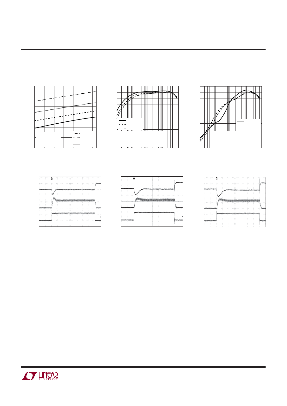
Burst Mode Operation Effi ciency vs Supply Voltage
Supply Current vs Temperature
Burst Mode Operation
TYPICAL PERFORMANCE CHARACTERISTICS
V
REF
vs Temperature at 2.25V,
3.6V, 5.5V
Switching Frequency vs Supply
Voltage and Temperature Load Regulation, All Channels
TEMPERATURE (°C)
–50
0.585
V
REF
(V)
0.590
0.595
0.600
0.605
0.610
0.615
0 50 100
3545 G01
2.25V
3.6V
5.5V
SUPPLY VOLTAGE (V)
2
1.5
SWITCHING FREQUENCY (MHz)
2.0
2.5
3.0
34
3545 G02
56
f
OSC
= –40°C
f
OSC
= 0°C
f
OSC
= 25°C
f
OSC
= 80°C
LOAD CURRENT (mA)
0
0.6
0.8
1.2
600
3545 G03
0.4
0.2
200 400 800
0
–0.4
–0.2
1.0
V
OUT
ERROR (%)
CHANNEL 1
CHANNEL 2
CHANNEL 3
TA = 25°C
V
IN
= 3.6V
UNTESTED CHANNELS OFF
PULSE SKIP MODE
1µs/DIV
SW
2V/DIV
I
L
100mA/DIV
V
OUT
20mV/DIV
3545 G04
VIN = 3.6V
V
OUT
= 1.8V
I
LOAD
= 50mA
f
OSC
= 2.25MHz
SUPPLY VOLTAGE (V)
2
EFFICIENCY (%)
90
95
6
3545 G05
85
80
3
4
5
100
V
OUT
= 2V
T
A
= 25°C
CHANNEL 3, ALL OTHERS OFF
f
OSC
= 2.25MHz
I
LOAD
= 250mA
TEMPERATURE (°C)
–40
0
SUPPLY CURRENT (µA)
5
15
20
25
40
45
3545 G06
10
0
–20
60
20 80
30
35
40
VIN = 5.5V
V
IN
= 4.5V
V
IN
= 3.5V
V
IN
= 2.5V
TA = 25°C
V
FB3
= 0.625V
I
LOAD
= 0V
CHANNEL 3 ONLY
Page 5
LTC3545/LTC3545-1
5
35451fa
TYPICAL PERFORMANCE CHARACTERISTICS
Channel 1 Load Step Response Channel 2 Load Step Response Channel 3 Load Step Response
Supply Current vs Temperature,
Pulse Skipping
Effi ciency vs Load Current,
Burst Mode Operation
Effi ciency vs Load Current,
Pulse Skipping Operation
TEMPERATURE (°C)
–40
150
SUPPLY CURRENT (µA)
200
250
300
350
450
–20
02040
3545 G07
60 80
400
TA = 25°C
V
FB3
= 0.625V
I
LOAD
= 0V
CHANNEL 3 ONLY
VIN = 5.5V
V
IN
= 4.5V
V
IN
= 3.5V
V
IN
= 2.5V
LOAD CURRENT (mA)
30
EFFICIENCY (%)
90
100
20
10
80
50
70
60
40
0.1 10 100 1000
3545 G08
0
1
VIN = 2.7V
V
IN
= 3.6V
V
IN
= 4.2V
TA = 25°C
V
OUT
= 1.8V
CHANNEL 3, OTHER CHANNELS OFF
f
OSC
= 2.25MHz
LOAD CURRENT (mA)
30
EFFICIENCY (%)
90
100
20
10
80
50
70
60
40
0.1 10 100 1000
3545 G09
0
1
VIN = 2.7V
V
IN
= 3.6V
V
IN
= 4.2V
TA = 25°C
V
OUT
= 1.8V
CHANNEL 3, OTHER CHANNELS OFF
f
OSC
= 2.25MHz
10µs/DIV
I
LOAD
500mA/DIV
I
L
500mA/DIV
V
OUT1
100mV/DIV
3545 G10
TA = 25°C
V
IN
= 3.6V
V
OUT
= 1.2V
LOAD STEP 0mA TO 600mA
Burst Mode OPERATION
10µs/DIV
I
LOAD
500mA/DIV
I
L
500mA/DIV
V
OUT2
100mV/DIV
3545 G11
TA = 25°C
V
IN
= 3.6V
V
OUT
= 1.5V
LOAD STEP 0mA TO 600mA
Burst Mode OPERATION
10µs/DIV
I
LOAD
500mA/DIV
I
L
500mA/DIV
V
OUT3
100mV/DIV
3545 G12
TA = 25°C
V
IN
= 3.6V
V
OUT
= 1.8V
LOAD STEP 0mA TO 600mA
Burst Mode OPERATION
Page 6
LTC3545/LTC3545-1
6
35451fa
TYPICAL PERFORMANCE CHARACTERISTICS
Start-Up From Shutdown
Loaded
PFET R
DS(ON)
vs Supply Voltage PFET R
DS(ON)
vs Temperature
NFET R
DS(ON)
vs Supply Voltage
Start-Up From Shutdown
No Load Load Step Crosstalk
NFET R
DS(ON)
vs Temperature
200µs/DIV
I
SUPPLY
1A/DIV
RUNX
5V/DIV
V
OUT1
V
OUT2
V
OUT3
(ALL 1V/DIV)
3545 G13
TA = 25°C
V
IN
= 3.6V
I
LOAD
= 600mA, ALL CHANNELS
200µs/DIV
I
SUPPLY
50mA/DIV
V
OUT1
1V/DIV
V
OUT2
1V/DIV
V
OUT3
1V/DIV
3545 G14
TA = 25°C
V
IN
= 3.6V
I
LOAD
= 0, ALL CHANNELS
200µs/DIV
I
LOAD
CH1
50mA/DIV
V
OUT2
2mV/DIV
V
OUT3
2mV/DIV
V
OUT1
100mV/DIV
3545 G15
TA = 25°C
V
IN
= 3.6V
500mA LOAD STEP IN CHANNEL1
CHANNELS 2 AND 3 LOADED AT 400mA EACH
SUPPLY VOLTAGE (V)
2
0
R
DS(ON)
()
0.05
0.15
0.20
0.25
0.50
0.35
3
4
3545 G16
0.10
0.40
0.45
0.30
5
6
TA = 85°C
T
A
= 25°C
T
A
= –25°C
TEMPERATURE (°C)
–50
0
R
DS(ON)
()
0.05
0.15
0.20
0.25
0.50
0.35
0
3545 G17
0.10
0.40
0.45
0.30
50
100
VIN = 2.5V
V
IN
= 3.6V
V
IN
= 5.5V
SUPPLY VOLTAGE (V)
2
0
R
DS(ON)
()
0.05
0.15
0.20
0.25
0.50
0.35
3
4
3545 G18
0.10
0.40
0.45
0.30
5
6
TA = 85°C
T
A
= 25°C
T
A
= –25°C
TEMPERATURE (°C)
–50
0
R
DS(ON)
()
0.05
0.15
0.20
0.25
0.50
0.35
0
3545 G19
0.10
0.40
0.45
0.30
50
100
VIN = 2.5V
V
IN
= 3.6V
V
IN
= 5.5V
Page 7

LTC3545/LTC3545-1
7
35451fa
PIN FUNCTIONS
SW1 (Pin 1): Switch Node Connection to Inductor for
Regulator 1. This pin connects to the internal power
MOSFET switches.
PGOOD1 (Pin 2): This open-drain output voltage is pulled
to a logic low when V
FB1
is below 0.55V (V
OUT1
is below
90% of regulated level).
RUN2 (Pin 3): Regulator 2 Enable Pin. Apply a voltage
greater than V
RUN(HIGH)
to enable this regulator.
PGOOD2 (Pin 4): This open-drain output voltage is pulled
to a logic low when V
FB2
is below 0.55V (V
OUT2
is below
90% of regulated level).
SW2 (Pin 5): Switch Node Connection to Inductor for
Regulator 2. This pin connects to the internal power
MOSFET switches.
PGND (Pin 6): Regulators 2 and 3 Power Path Return.
PV
IN
(Pin 7): Power Path Supply Pin for Regulators 2 and
3. This pin must be closely decoupled to PGND, with a
4.7µF or greater ceramic capacitor.
SW3 (Pin 8): Switch Node Connection to Inductor for
Regulator 3. This pin connects to the internal power
MOSFET switches.
SYNC/MODE (Pin 9, LTC3545 Only): Mode Select and
External Clock Input. When pulled low, part operates in
Burst Mode operation. When pulled high, part operates
in pulse skipping mode. When driven by a 1MHz to 3MHz
external clock, the part operates in pulse skipping mode
with a switching frequency equal to the external clock.
PGOOD3 (Pin 9, LTC3545-1 Only): This open-drain output
voltage is pulled to a logic low when V
FB3
is below 0.55V
(V
OUT3
is below 90% of regulated level). The LTC3545-1
operates in Burst Mode operation only.
RUN3 (Pin 10): Regulator 3 Enable Pin. Apply a voltage
greater than V
RUN(HIGH)
to enable this regulator.
V
FB3
(Pin 11): Regulator 3 Feedback Pin. This pin receives
the feedback voltage from an external resistive divider
across the output.
V
FB2
(Pin 12): Regulator 2 Feedback Pin. This pin receives
the feedback voltage from an external resistive divider
across the output.
V
FB1
(Pin 13): Regulator 1 Feedback Pin. This pin receives
the feedback voltage from an external resistive divider
across the output.
RUN1 (Pin 14): Regulator 1 Enable Pin. Apply a voltage
greater than V
RUN(HIGH)
to enable this regulator.
V
IN
(Pin 15): Supply Pin for Internal Reference and Control
Circuitry. Power path supply for regulator 1.
GNDA (Pin 16): Ground Pin for Internal Reference and
Control Circuitry. Power path return for regulator 1.
Exposed Pad (Pin 17): GND. Must be soldered to the
PCB.
Page 8

LTC3545/LTC3545-1
8
35451fa
FUNCTIONAL DIAGRAMS
I
BIAS3
PGOOD3
(LTC3545-1
ONLY)
POWER
REG3 REG1
V
FB3
SW3
I
BIAS2
PGOOD2
POWER
REG2
V
FB2
SW2
PGOOD1
V
FB1
SW1
PV
IN
PGND
0.8V
REF
OSC
V
IN
RUN2 SYNC/MODE
(LTC3545
ONLY)
RUN1RUN3 GNDA
SHDN
RUN
LOGIC
I
BIAS100
POWER
3545 FD01
Page 9

LTC3545/LTC3545-1
9
35451fa
FUNCTIONAL DIAGRAMS
–
+
–
+
–
+
EA
–
+
V
SLEEP
I
TH
SWITCHING
LOGIC
AND
BLANKING
CIRCUIT
S
R
Q
Q
RS
LATCH
BURST
–
+
I
COMP
I
RCMP
ANTI
SHOOT-
THRU
SLOPE
COMP
SLEEP
0.6V V
REF
OSC
OSC
SHUTDOWN
REGULATOR
SWX
10
3545 FD02
V
FBX
PGOOD
PV
IN
PGND
0.6V
0.6V
50mV
BURST
CLAMP
SOFT-START
+
Page 10

LTC3545/LTC3545-1
10
35451fa
OPERATION
MAIN CONTROL LOOP
The LTC3545/LTC3545-1 use a constant frequency, current
mode step-down architecture. Both the main (P-channel
MOSFET) and synchronous (N-channel MOSFET) switches
are internal. During normal operation, the internal top power
MOSFET is turned on each cycle when the oscillator sets
the RS latch, and turned off when the current comparator,
I
COMP
, resets the RS latch. The peak inductor current at
which I
COMP
resets the RS latch, is controlled by the output
of error amplifi er EA. When the load current increases, it
causes a slight decrease in the feedback voltage FB relative to the 0.6V reference, which in turn, causes the EA
amplifi er’s output voltage to increase until the average
inductor current matches the new load current. While the
top MOSFET is off, the bottom MOSFET is turned on until
either the inductor current starts to reverse, as indicated by
the current reversal comparator, I
RCMP
, or the beginning
of the next clock cycle.
PULSE SKIPPING/Burst Mode OPERATION
At light loads, the inductor current may reach zero or
reverse on each pulse. The bottom MOSFET is turned off
by the current reversal comparator, I
RCMP
, and the switch
voltage will ring. This is discontinuous mode operation,
and is normal behavior for the switching regulator.
At very light loads, the LTC3545/LTC3545-1 will automatically begin operating in either pulse skipping or Burst Mode
operation depending on the state of the MODE/SYNC pin
(LTC3545). In either case the part will begin to skip cycles
in order to maintain regulation.
In pulse skip mode, the current pulses are smaller and
more frequent, giving lower output ripple. In this mode,
internal circuitry remains on and the pulses occur more
frequently resulting in lower effi ciency than in Burst Mode
operation at light loads.
In Burst Mode operation, the part supplies fewer, larger
current pulses, resulting in higher output ripple, but much
higher light load effi ciency than pulse skip mode. Effi ciency
is also improved by turning off much of the internal circuitry
during the dead time between pulses.
Page 11

LTC3545/LTC3545-1
11
35451fa
Figure 1. Start-Up from Shutdown, No Load
SOFT-START
Soft-start reduces surge currents on V
IN
and output
overshoot during start-up. Soft-start on the LTC3545/
LTC3545-1 is implemented by internally ramping the reference signal fed to the error amplifi er over approximately a
1ms period. Figure 1 shows the behavior of the regulator
channels during start-up.
Short-Circuit Protection
Short-circuit protection is achieved by monitoring the inductor current. When the current exceeds a predetermined
level, the main switch is turned off, and the synchronous
switch is turned on long enough to allow the current in the
inductor to decay below the fault threshold. This prevents
a catastrophic inductor current run-away condition, but
will still provide current to the output. Output voltage
regulation in this condition is not achieved.
DROPOUT OPERATION
As the input supply voltage decreases to a value approaching the output voltage, the duty cycle increases toward the
maximum on-time. Further reduction of the supply voltage
forces the main switch to remain on for more than one
cycle until it reaches 100% duty cycle. The output voltage will then be determined by the input voltage minus
the voltage drop across the P-channel MOSFET and the
inductor. An important detail to remember is that at low
input supply voltages, the R
DS(ON)
of the P-channel switch
increases (see Typical Performance Characteristics).
Therefore, the user should calculate the power dissipation
when the LTC3545/LTC3545-1 is used at 100% duty cycle
with low input voltage (See Thermal Considerations in the
Applications Information section).
OPERATION
200µs/DIV
RUNX
2V/DIV
V
OUT1
V
OUT2
V
OUT3
(ALL 1V/DIV)
3545 F01
TA = 25°C
V
IN
= 3.6V
I
LOAD
= 0mA, ALL CHANNELS
Page 12

LTC3545/LTC3545-1
12
35451fa
APPLICATIONS INFORMATION
The basic LTC3545/LTC3545-1 application circuit is shown
on the fi rst page of this data sheet. External component
selection is driven by the load requirement and begins
with the selection of L followed by C
IN
and C
OUT
.
Inductor Selection
For most applications, the value of the inductor will fall in
the range of 1µH to 10µH. Its value is chosen based on the
desired ripple current. Large inductor values lower ripple
current and small inductor values result in higher ripple
currents. Higher V
IN
or V
OUT
also increases the ripple
current as shown in Equation 1. A reasonable starting
point for setting ripple current for an 800mA regulator is
ΔI
L
= 320mA (40% of 800mA).
ΔI
L
V
V
V
L OUT
OUT
IN
=
()()
⎛
⎝
⎜
⎞
⎠
⎟
1
1ƒ–
(1)
The DC current rating of the inductor should be at least equal
to the maximum load current plus half the ripple current
to prevent core saturation. Thus, a 960mA rated inductor
should be enough for most applications (800mA + 160mA).
For better effi ciency, choose a low DCR inductor.
Inductor Core Selection
Different core materials and shapes will change the
size/current and price/current relationship of an inductor. Toroid or shielded pot cores in ferrite or permalloy
materials are small and don’t radiate much energy, but
generally cost more than powdered iron core inductors
with similar electrical characteristics. The choice of which
style inductor to use often depends more on the price vs
size requirements and any radiated fi eld/EMI requirements
than on what the LTC3545/LTC3545-1 require to operate.
Table 1 shows typical surface mount inductors that work
well in LTC3545/LTC3545-1 applications.
C
IN
and C
OUT
Selection
In continuous mode, a worst-case estimate for the input
current ripple can be determined by assuming that the
source current of the top MOSFET is a square wave of
duty cycle V
OUT/VIN
, and amplitude I
OUT(MAX)
. To prevent
large voltage transients, a low ESR input capacitor sized for
the maximum RMS current must be used. The maximum
RMS capacitor current is given by:
II
VVV
V
RMS OUT MAX
OUT IN OUT
IN
≅
()
()
–
This formula has a maximum at VIN = 2V
OUT
, where I
RMS
= I
OUT
/2. This simple worst-case condition is commonly
used for design. Note that the capacitor manufacturer’s
ripple current ratings are often based on 2000 hours of
life (non-ceramic capacitors). This makes it advisable to
further de-rate the capacitor, or choose a capacitor rated
at a higher temperature than required. Always consult the
manufacturer if there is any question.
Table 1. Representative Surface Mount Inductors
PART
NUMBER
VALUE
(μH)
DCR
(Ω MAX)
MAX DC
CURRENT (A) W × L × H (mm3)
Wurth WETPC 744031
1.5
2.5
3.6
0.035
0.045
0.065
1.75
1.45
1.38
3.8 × 3.8 × 1.65
CoilCraft
LPS4012
1
1.5
2.2
3.3
0.06
0.07
0.1
0.1
2.5
2.5
2.1
1.5
4.0 × 4.0 × 1.1
Sumida
CDH38D11/
SLD
1.4
2.4
3.6
0.055
0.094
0.13
1.8
1.3
1.1
4.0 × 4.0 × 1.2
Sumida
CDRH3D16
1.5
2.2
3.3
0.043
0.075
0.11
1.55
1.2
1.1
3.8 × 3.8 × 1.8
Page 13

LTC3545/LTC3545-1
13
35451fa
The selection of C
OUT
is driven by the required effective
series resistance (ESR). Typically, once the ESR requirement for C
OUT
has been met, the RMS current rating
generally far exceeds the I
RIPPLE(P-P)
requirement. The
output ripple ΔV
OUT
is determined by:
ΔΔV I ESR
C
OUT L
OUT
≅+
⎛
⎝
⎜
⎞
⎠
⎟
1
8 ••ƒ
where f = operating frequency, C
OUT
= output capacitance
and ΔI
L
= ripple current in the inductor. For a fi xed output
voltage, the output ripple is highest at maximum input
voltage since ΔI
L
increases with input voltage.
Using Ceramic Input and Output Capacitors
Higher value, lower cost, ceramic capacitors are now
widely available in smaller case sizes. Their high ripple
current, high voltage rating and low ESR make them
ideal for switching regulator applications. Because the
LTC3545/LTC3545-1’s control loop does not depend on
the output capacitor’s ESR for stable operation, ceramic
capacitors can be used freely to achieve very low output
ripple and small circuit size.
However, care must be taken when ceramic capacitors are
used at the input and the output. When a ceramic capacitor
is used at the input and the power is supplied by a wall
adapter through long wires, a load step at the output can
induce ringing at the input, V
IN
. At best, this ringing can
couple to the output and be mistaken as loop instability. At
worst, a sudden inrush of current through the long wires
can potentially cause a voltage spike at V
IN
, large enough
to damage the part.
When choosing the input and output ceramic capacitors,
choose the X5R or X7R dielectric formulations. These
dielectrics have the best temperature and voltage characteristics of all the ceramics for a given value and size.
Output Voltage Programming
The output voltage is set by tying V
FB
to a resistive divider
according to the following formula:
VV
R
R
OUT
=+
⎛
⎝
⎜
⎞
⎠
⎟
06 1
2
1
.
The external resistive divider is connected to the output
allowing remote voltage sensing as shown in Figure 2.
APPLICATIONS INFORMATION
Figure 2. Setting the LTC3545 Output Voltage
Effi ciency Considerations
The effi ciency of a switching regulator is equal to the output
power divided by the input power times 100%. It is often
useful to analyze individual losses to determine what is
limiting the effi ciency and which change would produce
the most improvement. Effi ciency can be expressed as:
Effi ciency = 100% – (L1 + L2 + L3 + ...) where L1, L2, etc.
are the individual losses as a percentage of input power.
Although all dissipative elements in the circuit produce
losses, two main sources usually account for most of the
losses in LTC3545/LTC3545-1 circuits: V
IN
quiescent cur-
rent and I
2
R losses. VIN quiescent current loss dominates
the effi ciency loss at low load currents, whereas the I
2
R
loss dominates the effi ciency loss at medium to high load
currents. In a typical effi ciency plot, the effi ciency curve at
very low load currents can be misleading since the actual
power lost is of little consequence as illustrated on the
front page of the data sheet.
V
FB
GND
LTC3545
0.6V ≤ V
OUT
≤ 5.5V
R2
R1
3545 F02
Page 14

LTC3545/LTC3545-1
14
35451fa
1. The quiescent current is due to two components: the
DC bias current as given in the electrical characteristics
and the internal main switch and synchronous switch
gate charge currents. The gate charge current results
from switching the gate capacitance of the internal power
MOSFET switches. Each time the gate is switched from
high to low to high again, a packet of charge, dQ, moves
from PV
IN
to ground. The resulting dQ/dt is the current out
of PV
IN
that is typically larger than the DC bias current and
proportional to frequency. Both the DC bias and gate charge
losses are proportional to PV
IN
and thus their effects will
be more pronounced at higher supply voltages.
2. I
2
R losses are calculated from the resistances of the
internal switches, R
SW
, and external inductor RL. In continuous mode, the average output current fl owing through
inductor L is “chopped” between the main switch and the
synchronous switch. Thus, the series resistance looking
into the SW pin is a function of both top and bottom
MOSFET R
DS(ON)
and the duty cycle (DC) as follows:
R
SW
= (R
DS(ON)TOP
)(DC) + (R
DS(ON)BOT
)(1 – DC)
The R
DS(ON)
for both the top and bottom MOSFETs can
be obtained from the Typical Performance Characteristics
curves. Thus, to obtain I
2
R losses, simply add RSW to
R
L
and multiply the result by the square of the average
output current.
Other losses when in switching operation, including C
IN
and C
OUT
ESR dissipative losses and inductor core losses,
generally account for less than 2% total additional loss.
Thermal Considerations
The LTC3545/LTC3545-1 requires the package backplane
metal to be well soldered to the PC board. This gives the
QFN package exceptional thermal properties, making
it diffi cult in normal operation to exceed the maximum
junction temperature of the part. In most applications the
LTC3545/LTC3545-1 do not dissipate much heat due to
their high effi ciency. In applications where the LTC3545/
LTC3545-1 are running at high ambient temperature
with low supply voltage and high duty cycles, such as in
dropout, the heat dissipated may exceed the maximum
junction temperature of the part if it is not well thermally
grounded. If the junction temperature reaches approximately 150°C, the power switches will be turned off and
the SW nodes will become high impedance.
To prevent the LTC3545/LTC3545-1 from exceeding the
maximum junction temperature, the user will need to do
some thermal analysis. The goal of the thermal analysis
is to determine whether the power dissipated exceeds the
maximum junction temperature of the part. The temperature rise is given by:
T
R
= PD • θ
JA
where PD is the power dissipated by the regulator and θJA
is the thermal resistance from the junction of the die to
the ambient temperature.
The junction temperature, T
J
, is given by:
T
J
= TA + T
R
where TA is the ambient temperature.
As an example, consider one channel of the LTC3545/
LTC3545-1 in dropout at an input voltage of 2.5V, a load
current of 800mA, and an ambient temperature of 85°C.
From the typical performance graph of switch resistance,
the R
DS(ON)
of the P-channel switch at 85°C can be es-
timated as 0.42Ω. Therefore, power dissipated by the
channel is:
P
D
= I
LOAD
2
• R
DS(ON)
= 0.27W
The θ
JA
for the 3mm × 3mm QFN package is 68°C/W. The
temperature rise due to this power dissipation is:
T
R
= θJA • PD = 18°C
And a junction temperature of:
T
J
= 85°C + 18°C = 103°C
which is below the maximum junction temperature of
125°C. This would not be the case if all three channels
were operating at 800mA in dropout. Then T
R
= 55°C,
limiting the allowed ambient temperature in this scenario
to less than 70°C.
APPLICATIONS INFORMATION
Page 15

LTC3545/LTC3545-1
15
35451fa
Similar situations can occur when all three channels are
operating at maximum loads at high ambient temperature.
As an example, consider a channel supplying 800mA at
1.8V output and 85% effi ciency. The dissipated power can
be calculated using
Loss P
E
E
WW
O
=
⎛
⎝
⎜
⎞
⎠
⎟
==
1
14 017 025
–
.•. .
where PO is the output power and E is the effi ciency.
In this case the temperature rise is 17°C, similar to the
dropout scenario described above. Whereas one channel
operating at these levels will safely fall within the temperature limitations of the part, three channels operating
simultaneously at these levels will place limits on the peak
ambient temperature.
Note that at higher supply voltages, the junction temperature is lower due to reduced switch resistance R
DS(ON)
.
Checking Transient Response
The regulator loop response can be checked by looking
at the load transient response. Switching regulators take
several cycles to respond to a step in load current. When
a load step occurs, V
OUT
immediately shifts by an amount
equal to (ΔI
LOAD
• ESR), where ESR is the effective series
resistance of C
OUT
. ΔI
LOAD
also begins to charge or dis-
charge C
OUT
, which generates a feedback error signal. The
regulator loop then acts to return V
OUT
to its steady-state
value. During this recovery time V
OUT
can be monitored
for overshoot or ringing that would indicate a stability
problem. For a detailed explanation of switching control
loop theory, see Application Note 76.
A second, more severe transient is caused by switching
in loads with large (>1F) supply bypass capacitors. The
discharged bypass capacitors are effectively put in parallel with C
OUT
, causing a rapid drop in V
OUT
. No regulator
can deliver enough current to prevent this problem if the
load switch resistance is low and it is driven quickly. The
only solution is to limit the rise time of the switch drive
so that the load rise time is limited to approximately (25
• C
LOAD
). Thus, a 10F capacitor charging to 3.3V would
require a 250s rise time, limiting the charging current
to about 130mA.
APPLICATIONS INFORMATION
Design Example
As a design example, consider using the LTC3545/LTC35451 in a portable application with a Li-Ion battery. The battery
provides V
IN
ranging from 2.8V to 4.2V. The demand on
one channel at 2.5V is 600mA. Using this channel as an
example, fi rst calculate the inductor value for 40% ripple
current (240mA in this example) at maximum V
IN
. Using
a form of Equation 1:
L
V
MHz mA
V
V
1
25
2 25 240
1
25
36
14=
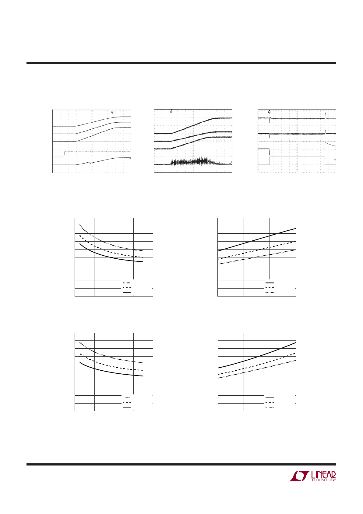
()()
⎛
⎝
⎜
⎞
⎠
⎟
=
.
.
–
.
.
.11µ H
Use the closest standard value of 1.5µH. For low ripple
applications, 10µF is a good choice for the output capacitor.
A smaller output capacitor will shorten transient response
settling time, but also increase the load transient ripple. A
value for C5 = 4.7µF should suffi ce as the source impedance of a Li-Ion battery is very low. C5 and C1 both provide
switching current to the output power switches. They
should be placed as close a possible to the chip between
VIN/GNDA and PVIN/PGND respectively. PVIN and PGND
are the supply and return power paths for both channels
2 and 3, so a value of 10µF for C1 is appropriate. The
feedback resistors program the output voltage. Minimizing the current in these resistors will maximize effi ciency
at very light loads, but totals on the order of 200k are a
good compromise between effi ciency and immunity to
any adverse effects of PCB parasitic capacitance on the
feedback pins. Choosing 10µA as the feedback current with
0.6V feedback voltage makes R4 = 60k. A close standard
1% resistor is 60.4k. Using:
R
V
V
Rk3
25
06
1 4 191 1=
⎛
⎝
⎜
⎞
⎠
⎟
=
.
.
–• .
The closest standard 1% resistor is 191k. A 20pF feedforward capacitor is recommended to improve transient
response. The component values for the other channels
are chosen in a similar fashion. Figure 4 shows the complete schematic for this example, along with the effi ciency
curve and burst mode ripple at an output current for the
2.5V output.
Page 16

LTC3545/LTC3545-1
16
35451fa
PC Board Layout Checklist
When laying out the printed circuit board, the following
checklist should be used to ensure proper operation of
the LTC3545/LTC3545-1. These items are also illustrated
graphically in Figures 3 and 4. Figure 3 shows the power
path components and traces. In this fi gure the feedback
networks are not shown since they reside on the bottom
side of the board. Check the following in your layout:
1. The power traces consisting of the PGND trace, the SW
trace, the PV
IN
trace, the VIN and GNDA traces, should
be kept short direct and wide.
2. Does each of the V
FBx
pins connect directly to the
respective feedback resistors? The resistive dividers
must be connected between the (+) plate of the cor-
responding output fi lter capacitor (e.g. C2) and GNDA.
If the circuit being powered is at such a distance from
the part where voltage drops along circuit traces are
large, consider a Kelvin connection from the powered
circuit back to the resistive dividers.
3. Keep C1 and C5 as close to the part as possible.
4. Keep the switching nodes (SWx) away from the sensitive V
FBx
nodes.
5. Keep the ground connected plates of the input and
output capacitors as close as possible.
6. Care should be taken to provide enough space between
unshielded inductors in order to minimize any transformer coupling.
APPLICATIONS INFORMATION
Figure 3. Layout Diagram
L3
L2L1
C2
C5
C1
C4
C3
V
OUT3
(VIA TO FEEDBACK
NETWORK)
(VIA TO FEEDBACK
NETWORK)
(VIA TO FEEDBACK
NETWORK)
V
OUT2
PGNDPV
IN
SW3
SW2SW1
V
OUT1
V
IN
GNDA
3545 F03
Page 17

LTC3545/LTC3545-1
17
35451fa
TYPICAL APPLICATIONS
Burst Mode Ripple
Overall Effi ciency vs
Channel 1 Load Current
Figure 4. LTC3545 Low Ripple Burst Mode Operation
CHANNEL 1 LOAD CURRENT (mA)
30
OVERALL EFFICIENCY (%)
90
100
20
10
80
50
70
60
40
0.1 10 100 1000
3545 TA03
0
1
TA = 25°C
V
IN
= 3.6V
V
OUT
= 2.5V
f
OSC
= 2.25MHz
CHANNEL 2 = 1.2V, I
LOAD
= 400mA
CHANNEL 3 = 1.5V, I
LOAD
= 400mA
1µs/DIV
I
L3
250mA/DIV
V
OUT3
AC COUPLED
20mV/DIV
SW3
2V/DIV
3545 TA04
TA = 25°C
V
IN
= 3.6V
V
OUT
= 1.5V
I
LOAD
= 50mA
f
OSC
= 2.25MHz
3545 TA02
L1
1.5µH
R1
511k
C2
10µF
6.3V
C1
10µF
10V
SW1
PGOOD1
RUN2
PGOOD2
SW2
PGND
P
VIN
SW3
GNDA
V
IN
RUN1
V
FB1
V
FB2
V
FB3
RUN3
SYNC/MODE
1
2
3
4
5
6
7
8
16
15
14
13
12
11
10
9
LTC3545
GND
17
R3
191k
C6
20pF
R4
60.4k
R5
100k
R6
100k
R7
165k
R8
110k
R2
511k
V
IN
2.7V TO 5.5V
C5
4.7µF
E3
V
OUT1
E2
PGOOD2E1PGOOD1
2.5V AT 0.8A
E4
GND
C3
10µF
6.3V
E7
V
OUT2
1.2V AT 0.8A
E6
GND
C4
10µF
6.3V
E5
V
OUT3
1.5V AT 0.8A
E8
GND
L2
1.5µH
L3
1.5µH
C7
20pF
C8
20pF
Page 18

LTC3545/LTC3545-1
18
35451fa
TYPICAL APPLICATIONS
3-Channel Power Sequencing
Figure 5. LTC3545-1 Three PGOODs and Power Sequencing
3545 TA05
L1
1.5µH
R1
511k
C2
10µF
SW1
PGOOD1
RUN2
PGOOD2
SW2
PGND
P
VIN
SW3
GNDA
V
IN
RUN1
V
FB1
V
FB2
V
FB3
RUN3
PGOOD3
1
2
3
4
5
6
7
8
16
15
14
13
12
11
10
9
LTC3545-1
GND
17
R3
100k
R4
100k
R5
165k
R6
110k
R7
133k
R8
66.5k
R2
511k
V
IN
2.5V TO 5.5V
R9
511k
E3
V
OUT1
E2
PGOOD2
E9
PGOOD3
E1
PGOOD1
1.2V AT 0.8A
E4
GND
C3
10µF
E7
V
OUT2
1.5V AT 0.8A
E6
GND
C4
10µF
E5
V
OUT3
1.8V AT 0.8A
E8
GND
L2
1.5µH
L3
1.5µH
C1
4.7µF
C6
20pF
C5
10µF
C7
20pF
C8
20pF
400µs/DIV
V
OUT1
RUN1
V
OUT2
V
OUT3
PGOOD3
3545 TA06
TA = 25°C
V
IN
= 3.6V
Page 19

LTC3545/LTC3545-1
19
35451fa
Information furnished by Linear Technology Corporation is believed to be accurate and reliable.
However, no responsibility is assumed for its use. Linear Technology Corporation makes no representation that the interconnection of its circuits as described herein will not infringe on existing patent rights.
3.00 p 0.10
(4 SIDES)
RECOMMENDED SOLDER PAD PITCH AND DIMENSIONS
1.65 p 0.05
(4 SIDES)
NOTE:
1. DRAWING CONFORMS TO JEDEC PACKAGE OUTLINE MO-220 VARIATION (WEED-4)
2. DRAWING NOT TO SCALE
3. ALL DIMENSIONS ARE IN MILLIMETERS
4. DIMENSIONS OF EXPOSED PAD ON BOTTOM OF PACKAGE DO NOT INCLUDE
MOLD FLASH. MOLD FLASH, IF PRESENT, SHALL NOT EXCEED 0.15mm ON ANY SIDE
5. EXPOSED PAD SHALL BE SOLDER PLATED
6. SHADED AREA IS ONLY A REFERENCE FOR PIN 1 LOCATION
ON THE TOP AND BOTTOM OF PACKAGE
PIN 1
TOP MARK
(NOTE 6)
0.40 p 0.10
BOTTOM VIEW—EXPOSED PAD
1.65 p 0.10
(4-SIDES)
0.75 p 0.05
R = 0.115
TYP
0.25 p 0.05
1
PIN 1 NOTCH R = 0.20 TYP
OR 0.25 s 45o CHAMFER
15 16
2
0.50 BSC
0.200 REF
2.10 p 0.05
3.50 p 0.05
0.70 p0.05
0.00 – 0.05
(UD16 VAR A) QFN 1207 REV A
0.25 p0.05
0.50 BSC
PACKAGE OUTLINE
UD Package
16-Lead Plastic QFN (3mm s 3mm)
(Reference LTC DWG # 05-08-1700 Rev A)
Exposed Pad Variation AA
PACKAGE DESCRIPTION
Page 20

LTC3545/LTC3545-1
20
35451fa
Linear Technology Corporation
1630 McCarthy Blvd., Milpitas, CA 95035-7417
(408) 432-1900 ● FAX: (408) 434-0507 ● www.linear.com
© LINEAR TECHNOLOGY CORPORATION 2008
LT 0408 REV A • PRINTED IN USA
RELATED PARTS
PART NUMBER DESCRIPTION COMMENTS
LTC3405/LTC3405A 300mA I
OUT
, 1.5MHz, Synchronous Step-Down DC/DC
Converters
95% Effi ciency, VIN: 2.5V to 5.5V, V
OUT(MIN)
= 0.8V, IQ = 20µA,
I
SD
< 1µA, ThinSOTTM Package
LTC3406/LTC3406B 600mA I
OUT
, 1.5MHz, Synchronous Step-Down DC/DC
Converters
96% Effi ciency, VIN: 2.5V to 5.5V, V
OUT(MIN)
= 0.6V, IQ = 20µA,
I
SD
< 1µA, ThinSOT Package
LTC3407/LTC3407-2 Dual 600mA/800mA I
OUT
, 1.5MHz/2.25MHz,
Synchronous Step-Down DC/DC Converters
95% Effi ciency, VIN: 2.5V to 5.5V, V
OUT(MIN)
= 0.6V, IQ = 40µA,
I
SD
< 1µA, 10-Lead MSE, DFN Packages
LTC3409 600mA I
OUT
, 1.7MHz/2.6MHz, Synchronous Step-Down
DC/DC Converter
96% Effi ciency, VIN: 1.6V to 5.5V, V
OUT(MIN)
= 0.6V, IQ = 65µA,
I
SD
< 1µA, DFN Package
LTC3410/LTC3410B 300mA I
OUT
, 2.25MHz, Synchronous Step-Down DC/DC
Converters
95% Effi ciency, VIN: 2.5V to 5.5V, V
OUT(MIN)
= 0.8V, IQ = 26µA,
I
SD
< 1µA, SC70 Package
LTC3411 1.25A I
OUT
, 4MHz, Synchronous Step-Down DC/DC
Converter
95% Effi ciency, VIN: 2.5V to 5.5V, V
OUT(MIN)
= 0.8V, IQ = 60µA,
I
SD
< 1µA, 10-Lead MSE, DFN Packages
LTC3412 2.5A I
OUT
, 4MHz, Synchronous Step-Down DC/DC
Converter
95% Effi ciency, VIN: 2.5V to 5.5V, V
OUT(MIN)
= 0.8V, IQ = 60µA,
I
SD
< 1µA, 16-Lead TSSOPE Package
LTC3419 Dual 600mA, 2.25MHz, Synchronous Step-Down DC/DC
Converter
96% Effi ciency, V
IN
: 2.5V to 5.5V, V
OUT(MIN)
= 0.6V, IQ = 35µA,
I
SD
< 1µA, MS10, 3mm × 3mm DFN Package
LTC3441/LTC3442
LTC3443
1.2A I
OUT
, 2MHz, Synchronous Buck-Boost DC/DC
Converters
95% Effi ciency, VIN: 2.4V to 5.5V, V
OUT(MIN)
: 2.4V to 5.25V, IQ = 50µA,
I
SD
< 1µA, DFN Package
LTC3531/LTC3531-3
LTC3531-3.3
200mA I
OUT
, 1.5MHz, Synchronous Buck-Boost DC/DC
Converters
95% Effi ciency, VIN: 1.8V to 5.5V, V
OUT(MIN)
: 2V to 5V, IQ = 16µA,
I
SD
< 1µA, ThinSOT, DFN Packages
LTC3532 500mA I
OUT
, 2MHz, Synchronous Buck-Boost DC/DC
Converter
95% Effi ciency, VIN: 2.4V to 5.5V, V
OUT(MIN)
: 2.4V to 5.25V, IQ = 35µA,
I
SD
< 1µA, 10-Lead MSE, DFN Packages
LTC3544/LTC3544B
300mA, 2 × 200mA, 100mA, 2.25MHz Quad
Synchronous Step-Down DC/DC Converter
95% Effi ciency, V
IN
: 2.5V to 5.5V, V
OUT(MIN)
= 0.8V, IQ = 60µA,
I
SD
< 1µA, 3mm × 3mm QFN Package
LTC3547 Dual 300mA I
OUT
, 2.25MHz, Synchronous Step-Down
DC/DC Converter
95% Effi ciency, VIN: 2.5V to 5.5V, V
OUT(MIN)
= 0.6V, IQ = 40µA,
I
SD
< 1µA, 8-Lead DFN Package
LTC3548/LTC3548-1
LTC3548-2
Dual 400mA/800mA I
OUT
, 2.25MHz, Synchronous
Step-Down DC/DC Converters
95% Effi ciency, VIN: 2.5V to 5.5V, V
OUT(MIN)
= 0.6V, IQ = 40µA,
I
SD
< 1µA, 10-Lead MSE, DFN Packages
LTC3561 1.25A I
OUT
, 4MHz, Synchronous Step-Down DC/DC
Converter
95% Effi ciency, VIN: 2.5V to 5.5V, V
OUT(MIN)
= 0.8V, IQ = 240µA,
I
SD
< 1µA, DFN Package
 Loading...