

Page 1
FEATURES
■
Up to 92% Efficiency
■
Generates 3.3V at 100mA from a Single AA Cell
■
Low Start-Up Voltage: 0.85V
■
1.2MHz Fixed Frequency Switching
■
Internal Synchronous Rectifier
■
2.5V to 5V Output Range
■
Automatic Burst Mode® Operation (LTC3400)
■
Continuous Switching at Light Loads (LTC3400B)
■
Logic Controlled Shutdown (<1µA)
■
Antiringing Control Minimizes EMI
■
Tiny External Components
■
Low Profile (1mm) ThinSOTTM Package
U
APPLICATIO S
■
Pagers
■
MP3 Players
■
Digital Cameras
■
LCD Bias Supplies
■
Handheld Instruments
■
Wireless Handsets
■
GPS Receivers
LTC3400/LTC3400B
600mA, 1.2MHz Micropower
Synchronous Boost Converter
in ThinSOT
U
DESCRIPTIO
The LTC®3400/LTC3400B are synchronous, fixed frequency, step-up DC/DC converters delivering high efficiency in a 6-lead ThinSOT package. Capable of supplying
3.3V at 100mA from a single AA cell input, the devices
contain an internal NMOS switch and PMOS synchronous
rectifier.
A switching frequency of 1.2MHz minimizes solution
footprint by allowing the use of tiny, low profile inductors
and ceramic capacitors. The current mode PWM design is
internally compensated, reducing external parts count.
The LTC3400 features automatic shifting to power saving
Burst Mode operation at light loads, while the LTC3400B
features continuous switching at light loads. Antiringing
control circuitry reduces EMI concerns by damping the
inductor in discontinuous mode, and the devices feature
low shutdown current of under 1µA.
Both devices are available in the low profile (1mm) ThinSOT
package.
, LTC, LT and Burst Mode are registered trademarks of Linear Technology Corporation.
ThinSOT is a trademark of Linear Technology Corporation.
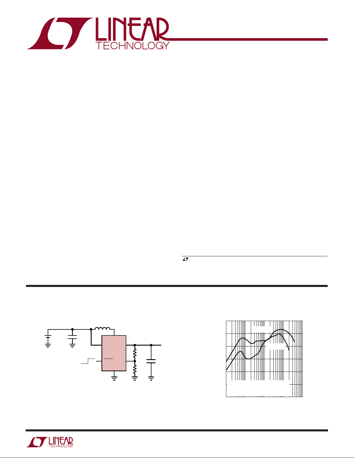
TYPICAL APPLICATIO
L1
4.7µH
+
SINGLE
AA CELL
C1, C2: TAIYO-YUDEN X5R EMK316BJ475ML
L1: COILCRAFT DO160C-472
Figure 1. Single Cell to 3.3V Synchronous Boost Converter
C1
4.7µF
OFF
ON
6
4
V
IN
LTC3400
SHDN
SW
GND
U
Efficiency
100
1
V
C2
4.7µF
3400 F01
OUT
3.3V
100mA
5
V
OUT
2
R1
1.02M
1%
3
FB
R2
604k
1%
90
80
70
EFFICIENCY (%)
60
FIGURE 1 CIRCUIT
50
WITH OPTIONAL SCHOTTKY DIODE
(SEE APPLICATIONS INFORMATION)
40
0.1 10 100 1000
VIN = 2.4V
VIN = 1.5V
1
LOAD CURRENT (mA)
3400 F01a
3400f
1
Page 2
LTC3400/LTC3400B
PACKAGE/ORDER I FOR ATIO
UU
W
WWWU
ABSOLUTE AXI U RATI GS
(Note 1)
VIN Voltage ................................................. –0.3V to 6V
SW Voltage ................................................. –0.3V to 6V
SHDN, FB Voltage ....................................... –0.3V to 6V
V
........................................................... –0.3V to 6V
OUT
Operating Temperature Range (Note 2) .. – 30°C to 85°C
Storage Temperature Range ................... – 65°C to 125°
Lead Temperature (Soldering, 10 sec)..................300°C
ORDER PART
TOP VIEW
SW 1
GND 2
FB 3
S6 PACKAGE
6-LEAD PLASTIC SOT-23
T
= 125°C, θJA = 256°C/W
JMAX
6 V
IN
5 V
OUT
4 SHDN
NUMBER
LTC3400ES6
LTC3400BES6
S6 PART MARKING
LTWK
LTUN
Consult LTC Marketing for parts specified with wider operating temperature ranges.
ELECTRICAL CHARACTERISTICS
temperature range, otherwise specifications are at TA = 25°C. VIN = 1.2V, V
PARAMETER CONDITIONS MIN TYP MAX UNITS
Minimum Start-Up Voltage I
Minimum Operating Voltage SHDN = VIN (Note 4) 0.5 0.65 V
Output Voltage Adjust Range 2.5 5 V
Feedback Voltage ● 1.192 1.23 1.268 V
Feedback Input Current VFB = 1.25V (Note 3) 1 nA
Quiescent Current (Burst Mode Operation) VFB = 1.4V (Note 5), LTC3400 Only 19 30 µA
Quiescent Current (Shutdown) V
Quiescent Current (Active) Measured On V
NMOS Switch Leakage VSW = 5V 0.1 5 µA
PMOS Switch Leakage VSW = 0V 0.1 5 µA
NMOS Switch On Resistance V
PMOS Switch On Resistance V
NMOS Current Limit 600 850 mA
Burst Mode Operation Current Threshold LTC3400 Only (Note 3) 3 mA
Current Limit Delay to Output (Note 3) 40 ns
Max Duty Cycle VFB = 1.15V ● 80 87 %
Switching Frequency 0.95 1.2 1.5 MHz
SHDN Input High 1V
SHDN Input Low 0.35 V
SHDN Input Current V
LOAD
SHDN
OUT
V
OUT
OUT
V
OUT
SHDN
The ● denotes the specifications which apply over the full operating
= 3.3V, unless otherwise specified.
OUT
= 1mA 0.85 1 V
= 0V, Not Including Switch Leakage 0.01 1 µA
OUT
= 3.3V 0.35 Ω
= 5V 0.20 Ω
= 3.3V 0.45 Ω
= 5V 0.30 Ω
● 0.85 1.2 1.5 MHz
= 5.5V 0.01 1 µA
300 500 µA
Note 1: Absolute Maximum Ratings are those values beyond which the life
of a device may be impaired.
Note 2: The LTC3400E/LTC3400BE are guaranteed to meet performance
specifications from 0°C to 70°C. Specifications over the –30°C to 85°C
operating temperature range are assured by design, characterization and
correlation with statistical process controls.
2
Note 3: Specification is guaranteed by design and not 100% tested in
production.
Note 4: Minimum V
battery’s ability to provide the necessary power as it enters a deeply
discharged state.
Note 5: Burst Mode operation I
by V
to get the equivalent input (battery) current.
OUT/VIN
operation after start-up is only limited by the
IN
is measured at V
Q
. Multiply this value
OUT
3400f
Page 3
UW
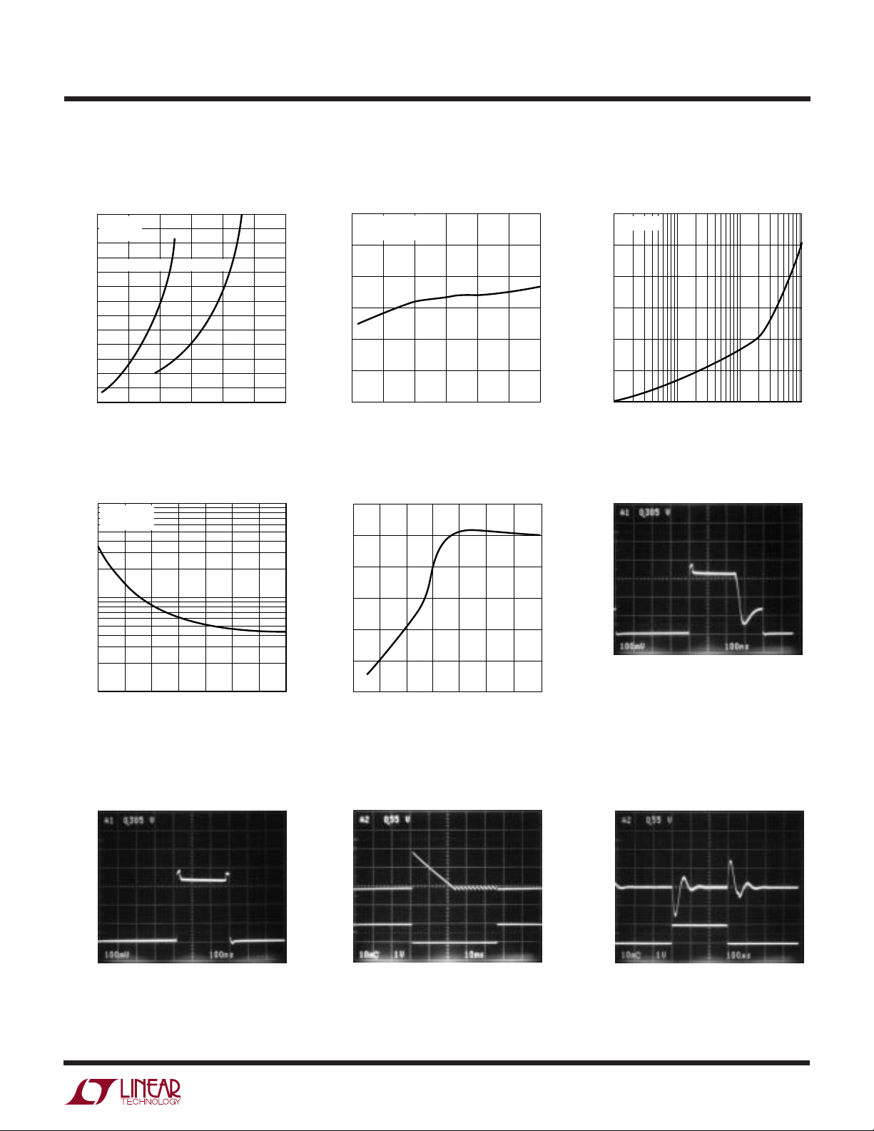
TYPICAL PERFOR A CE CHARACTERISTICS
LTC3400/LTC3400B
Output Load Burst Mode Threshold
vs V
IN
L = 4.7µH
= 25°C
T
A
20
V
= 3.3V V
OUT
10
OUTPUT CURRENT (mA)
0
0.9
1.5 2.1 2.7 3.3
OUT
VIN (V)
= 5V
No Load Battery Current vs V
1000
V
= 3.3V
OUT
= 25°C
T
A
100
3.9 4.5
3400 G01
BATT
V
vs Temperature
OUT
3.36
FIGURE 1 CIRCUIT
I
= 10mA
O
3.34
3.32
(V)
3.30
OUT
V
3.28
3.26
3.24
–60
03060
–30
TEMPERATURE (°C)
Normalized Oscillator Frequency
vs Temperature
1.01
1.00
0.99
0.98
90 120
3400 G02
Minimum Start-Up Voltage
vs Load Current
1.4
TA = 25°C
1.3
1.2
1.1
1.0
START-UP VOLTAGE (V)
0.9
0.8
0.1
1 10 100
I
(mA) CURRENT SOURCE LOAD
OUT
SW Pin Antiringing Operation
V
SW
1V/DIV
3400 G03
BATTERY CURRENT (µA)
10
0.9
1.2
1.8
BATTERY VOLTAGE (V)
SW Pin Fixed Frequency,
Continuous Inductor Current
Operation
V
SW
1V/DIV
0V
= 1.3V 100ns/DIV 3400 G07
V
IN
V
= 3.3V
OUT
= 50mA
I
OUT
L = 6.8µH
C
= 4.7µF
OUT
2.1 2.4 2.7
3400 G04
3.01.5
0.97
NORMALIZED FREQUENCY
0.96
0.95
–50
–30 –10
Fixed Frequency and Burst Mode
Operation V
V
OUT(AC)
100mV/DIV
60mA
I
OUT
10µA
V
= 1.3V 10ms/DIV 3400 G08
IN
V
= 3.3V
OUT
= 60mA TO 10µA
I
OUT
L = 6.8µH
C
= 4.7µF
OUT
30 70 90
10 50
TEMPERATURE (°C)
3400 G05
0V
V
OUT(AC)
100mV/DIV
100mA
I
OUT
40mA
= 1.3V 100ns/DIV 3400 G06
V
IN
V
= 3.3V
OUT
I
= 10mA
OUT
L = 6.8µH
= 4.7µF
C
OUT
Transient Response
OUT
V
= 1.3V 100µs/DIV 3400 G09
IN
V
= 3.3V
OUT
= 40mA TO 100mA
I
OUT
L = 6.8µH
C
= 4.7µF
OUT
3400f
3
Page 4
LTC3400/LTC3400B
U
UU
PI FU CTIO S
SW (Pin 1): Switch Pin. Connect inductor between SW
and VIN. Optional Schottky diode is connected between
SW and V
wide as possible to reduce EMI and voltage overshoot. If
the inductor current falls to zero, or SHDN is low, an
internal 100Ω antiringing switch is connected from SW to
VIN to minimize EMI.
GND (Pin 2): Signal and Power Ground. Provide a short
direct PCB path between GND and the (–) side of the output
capacitor(s).
FB (Pin 3): Feedback Input to the gm Error Amplifier.
Connect resistor divider tap to this pin. The output voltage
can be adjusted from 2.5V to 5V by:
V
OUT
SHDN (Pin 4): Logic Controlled Shutdown Input.
SHDN = High: Normal free running operation, 1.2MHz
typical operating frequency.
. Keep these PCB trace lengths as short and
OUT
= 1.23V • [1 + (R1/R2)]
SHDN = Low: Shutdown, quiescent current <1µA.
100Ω connected between SW and VIN.
Typically, SHDN should be connected to VIN through a 1M
pull-up resistor.
V
(Pin 5): Output Voltage Sense Input and Drain of the
OUT
Internal Synchronous Rectifier MOSFET. Bias is derived
from V
capacitor(s) should be as short and wide as possible. V
. PCB trace length from V
OUT
to the output filter
OUT
OUT
is held at VIN – 0.6V in shutdown due to the body diode of
the internal PMOS.
VIN (Pin 6): Battery Input Voltage. The device gets its
start-up bias from VIN. Once V
comes from V
. Thus, once started, operation is com-
OUT
exceeds VIN, bias
OUT
pletely independent from VIN. Operation is only limited by
the output power level and the battery’s internal series
resistance.
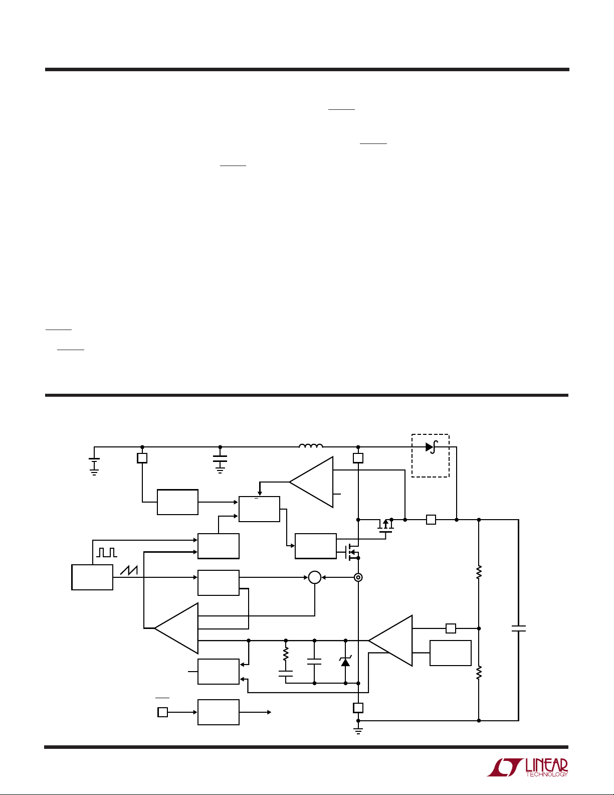
BLOCK DIAGRA
SINGLE
+
RAMP
GEN
1.2MHz
CELL
INPUT
V
6
IN
COMPARATOR
START-UP
PWM
SLEEP
OSC
W
CONTROL
SLOPE
+
–
–
Burst Mode
OPERATION
CONTROL
PWM
COMP
C
1µF
L1
4.7µH
IN
+
V
OUT
GOOD
–
A/B
A
MUX
B
SYNC
DRIVE
CONTROL
Σ
R
C
80k
C
C
150pF
C
P2
2.5pF
2.3V
SW
1
0.35Ω
CURRENT
SENSE
0.45Ω
g
m
ERROR
AMP
OPTIONAL
SCHOTTKY
–
+
FB
3
1.23V
REF
3.3V
OUTPUT
R1
1.02M
1%
(EXTERNAL)
R2
604k
1%
(EXTERNAL)
C
OUT
4.7µF
V
OUT
5
4
SHDN
4
SHUTDOWN
CONTROL
SHUTDOWN
2
GND
3400 BD
3400f
Page 5

OPERATIO
LTC3400/LTC3400B
U
The LTC3400/LTC3400B are 1.2MHz, synchronous boost
converters housed in a 6-lead ThinSOT package. Able to
operate from an input voltage below 1V, the devices
feature fixed frequency, current mode PWM control for
exceptional line and load regulation. With its low R
and gate charge internal MOSFET switches, the devices
maintain high efficiency over a wide range of load current.
Detailed descriptions of the three distinct operating modes
follow. Operation can be best understood by referring to
the Block Diagram.
Low Voltage Start-Up
The LTC3400/LTC3400B will start up at a typical VIN voltage of 0.85V or higher. The low voltage start-up circuitry
controls the internal NMOS switch up to a maximum peak
inductor current of 850mA (typ), with an approximate
1.5µs off-time during start-up, allowing the devices to
start up into an output load. Once V
start-up circuitry is disabled and normal fixed frequency
PWM operation is initiated. In this mode, the LTC3400/
LTC3400B operate independent of VIN, allowing extended
operating time as the battery can droop to several tenths
of a volt without affecting output voltage regulation. The
limiting factor for the application becomes the ability of the
battery to supply sufficient energy to the output.
Low Noise Fixed Frequency Operation
Oscillator: The frequency of operation is internally set to
1.2MHz.
Error Amp: The error amplifier is an internally compensated
transconductance type (current output) with a transconductance (gm) = 33 microsiemens. The internal 1.23V reference
voltage is compared to the voltage at the FB pin to generate
an error signal at the output of the error amplifier. A voltage divider from V
voltage via FB from 2.5V to 5V using the equation:
V
= 1.23V • [1 + (R1/R2)]
OUT
Current Sensing: A signal representing NMOS switch
current is summed with the slope compensator. The
summed signal is compared to the error amplifier output
to provide a peak current control command for the PWM.
Peak switch current is limited to approximately 850mA
to ground programs the output
OUT
exceeds 2.3V, the
OUT
DS(ON)
independent of input or output voltage. The current signal
is blanked for 40ns to enhance noise rejection.
Zero Current Comparator: The zero current comparator
monitors the inductor current to the output and shuts off
the synchronous rectifier once this current reduces to approximately 20mA. This prevents the inductor current from
reversing in polarity improving efficiency at light loads.
Antiringing Control: The antiringing control circuitry prevents high frequency ringing of the SW pin as the inductor
current goes to zero by damping the resonant circuit
formed by L and C
Burst Mode Operation
Portable devices frequently spend extended time in low
power or standby mode, only switching to high power
drain when specific functions are enabled. In order to
improve battery life in these types of products, high power
converter efficiency needs to be maintained over a wide
output power range. In addition to its high efficiency at
moderate and heavy loads, the LTC3400 includes automatic Burst Mode operation that improves efficiency of
the power converter at light loads. Burst mode operation
is initiated if the output load current falls below an
internally programmed threshold (see Typical Performance graph, Output Load Burst Mode Threshold vs VIN).
Once initiated, the Burst Mode operation circuitry shuts
down most of the device, only keeping alive the circuitry
required to monitor the output voltage. This is referred to
as the sleep state. In sleep, the LTC3400 draws only 19µA
from the output capacitor, greatly en
When the output voltage has drooped approximately 1%
from nominal, the LTC3400 wakes up and commences
normal PWM operation. The output capacitor recharges
and causes the LTC3400 to reenter sleep if the output load
remains less than the sleep threshold. The frequency of
this intermittent PWM or burst operation is proportional to
load current; that is, as the load current drops further
below the burst threshold, the LTC3400 turns on less
frequently. When the load current increases above the
burst threshold, the LTC3400 will resume continuous
PWM operation seamlessly. The LTC3400B does not use
Burst Mode operation and features continous operation at
light loads, eliminating low frequency output voltage ripple
at the expense of light load efficiency.
(capacitance on SW pin).
SW
hancing efficiency.
3400f
5
Page 6

LTC3400/LTC3400B
INDUCTANCE (µH)
3
60
OUTPUT CURRENT (mA)
80
110
120
160
7
11
13 21
180
140
59
15
17
19
23
3400 F03
V
IN
=1.2V
V
OUT
= 3V
V
OUT
= 3.3V
V
OUT
= 3.6V
V
OUT
= 5V
WUUU
APPLICATIO S I FOR ATIO
PCB LAYOUT GUIDELINES
The high speed operation of the LTC3400/LTC3400B
demands careful attention to board layout. You will not get
advertised performance with careless layout. Figure 2
shows the recommended component placement. A large
ground pin copper area will help to lower the chip temperature. A multilayer board with a separate ground plane is
ideal, but not absolutely necessary.
(OPTIONAL)
SW
V
IN
1
GND
2
6
V
IN
V
5
OUT
Figure 3. Maximum Output Current vs
Inductance Based On 90% Efficiency
COMPONENT SELECTION
Inductor Selection
The LTC3400/LTC3400B can utilize small surface mount
and chip inductors due to their fast 1.2MHz switching
frequency. A minimum inductance value of 3.3µH is
necessary for 3.6V and lower voltage applications and
4.7µH for output voltages greater than 3.6V. Larger values
of inductance will allow greater output current capability
by reducing the inductor ripple current. Increasing the
inductance above 10µH will increase size while providing
little improvement in output current capability.
The approximate output current capability of the LTC3400/
LTC3400B versus inductance value is given in the equation below and illustrated graphically in Figure 3.
SHDN
FB
3
RECOMMENDED COMPONENT PLACEMENT. TRACES
CARRYING HIGH CURRENT ARE DIRECT. TRACE AREA AT
FB PIN IS SMALL. LEAD LENGTH TO BATTERY IS SHORT
3400 F02
4
V
OUT
SHDN
Figure 2. Recommended Component Placement
for Single Layer Board
VD
II
OUT MAX P
()
•–
η
•
IN
fL
••
2
D
•–=
1
()
where:
η = estimated efficiency
IP = peak current limit value (0.6A)
VIN = input (battery) voltage
D = steady-state duty ratio = (V
– VIN)/V
OUT
OUT
f = switching frequency (1.2MHz typical)
L = inductance value
The inductor current ripple is typically set for 20% to 40%
of the maximum inductor current (IP). High frequency
ferrite core inductor materials reduce frequency dependent power losses compared to cheaper powdered iron
types, improving efficiency. The inductor should have low
ESR (series resistance of the windings) to reduce the I2R
power losses, and must be able to handle the peak
inductor current without saturating. Molded chokes and
some chip inductors usually do not have enough core to
support the peak inductor currents of 850mA seen on the
LTC3400/LTC3400B. To minimize radiated noise, use a
toroid, pot core or shielded bobbin inductor. See Table 1
for some suggested components and suppliers.
3400f
6
Page 7

WUUU
APPLICATIO S I FOR ATIO
LTC3400/LTC3400B
Table 1. Recommended Inductors
MAX
L DCR HEIGHT
PART (µH) mΩ (mm) VENDOR
CDRH5D18-4R1 4.1 57 2.0 Sumida
CDRH5D18-100 10 124 2.0 (847) 956-0666
CDRH3D16-4R7 4.7 105 1.8 www.sumida.com
CDRH3D16-6R8 170 1.8
CR43-4R7 4.7 109 3.5
CR43-100 10 182 3.5
CMD4D06-4R7MC 4.7 216 0.8
CMD4D06-3R3MC 3.3 174 0.8
DS1608-472 4.7 60 2.9 Coilcraft
DS1608-103 10 75 2.9 (847) 639-6400
DO1608C-472 4.7 90 2.9 www.coilcraft.com
D52LC-4R7M 4.7 84 2.0 Toko
D52LC-100M 10 137 2.0 (408) 432-8282
www.tokoam.com
LQH3C4R7M24 4.7 195 2.2 Murata
www.murata.com
Output and Input Capacitor Selection
Low ESR (equivalent series resistance) capacitors should
be used to minimize the output voltage ripple. Multilayer
ceramic capacitors are an excellent choice as they have
extremely low ESR and are available in small footprints. A
2.2µF to 10µF output capacitor is sufficient for most
applications. Larger values up to 22µF may be used to
obtain extremely low output voltage ripple and improve
transient response. An additional phase lead capacitor
may be required with output capacitors larger than 10µF
to maintain acceptable phase margin. X5R and X7R
dielectric materials are preferred for their ability to maintain capacitance over wide voltage and temperature ranges.
Low ESR input capacitors reduce input switching noise
and reduce the peak current drawn from the battery. It
follows that ceramic capacitors are also a good choice for
input decoupling and should be located as close as possible to the device. A 4.7µF input capacitor is sufficient for
virtually any application. Larger values may be used without limitations. Table 2 shows a list of several ceramic
capacitor manufacturers. Consult the manufacturers directly for detailed information on their entire selection of
ceramic parts.
Table 2. Capacitor Vendor Information
SUPPLIER PHONE WEBSITE
AVX (803) 448-9411 www.avxcorp.com
Murata (714) 852-2001 www.murata.com
Taiyo Yuden (408) 573-4150 www.t-yuden.com
Output Diode
Use a Schottky diode such as an MBR0520L, CMDSH2-3,
1N5817 or equivalent if the converter output voltage is 4.5V
or greater. The Schottky diode carries the output current for
the time it takes for the synchronous rectifier to turn on. Do
not use ordinary rectifier diodes, since the slow recovery
times will compromise efficiency. A Schottky diode is
optional for output voltages below 4.5V, but will increase
converter efficiency by 2% to 3%.
3400f
7
Page 8

LTC3400/LTC3400B
TYPICAL APPLICATIO S
U
Single Cell to 3.3V Synchronous Boost Converter
with Load Disconnect in Shutdown
+
SINGLE
AA CELL
OFF
ON
D1: CENTRAL SEMI CMDSH2-3
L1: COILCRAFT DS1608-472
C1
4.7µF
L1
4.7µH
6
4
V
IN
LTC3400
SHDN
SW
GND
1
V
2
OUT
FB
R3
510k
D1
M1
R3
510k
C2
4.7µF
Si2305DS
Q1
2N3904
3400 TA01a
5
3
R1
1.02M
1%
R2
604k
1%
V
OUT
3.3V
100mA
8
3400f
Page 9

TYPICAL APPLICATIO S
LTC3400/LTC3400B
U
Single Lithium Cell to 5V, 250mA
+
LITHIUM
CELL
D1: CENTRAL SEMI CMDSH2-3
L1: SUMIDA CMD4D06-4R7
OFF
C1
4.7µF
ON
3.6V to 5V Efficiency
100
LTC3400
= 4.7µF
C
O
L = 4.7µH
90
80
70
EFFICIENCY (%)
60
L1
4.7µH
6
V
4
SHDN
SW
IN
LTC3400
GND
D1
1
5
V
OUT
3
FB
2
C2
4.7µF
R1
1.82M
1%
R2
604k
1%
3400 TA02a
50
0.1 10 100 1000
1
LOAD CURRENT (mA)
3400 TA02b
3400f
9
Page 10

LTC3400/LTC3400B
TYPICAL APPLICATIO S
Single Cell AA Cell to ±3V Synchronous Boost Converter
U
L1
4.7µH
+
SINGLE
AA CELL
D1, D2: ZETEX FMND7000 DUAL DIODE
L1: COILCRAFT DS1608-472
OFF
C1
4.7µF
ON
6
4
V
IN
LTC3400
SHDN
SW
GND
C3
1µF
1
V
C2
4.7µF
3400 TA03a
OUT1
3V
90mA
V
OUT2
–3V
10mA
5
V
OUT
2
R1
1.02M
1%
3
FB
R2
750k
1%
D1 D2
C4
10µF
10
3400f
Page 11

PACKAGE DESCRIPTIO
0.754
U
S6 Package
6-Lead Plastic SOT-23
(Reference LTC DWG # 05-08-1636)
0.854 ±0.127
LTC3400/LTC3400B
2.90 BSC
(NOTE 4)
3.254
0.95 BSC
1.9 BSC
RECOMMENDED SOLDER PAD LAYOUT
0.20 BSC
DATUM ‘A’
0.30 – 0.50 REF
NOTE:
1. DIMENSIONS ARE IN MILLIMETERS
2. DRAWING NOT TO SCALE
3. DIMENSIONS ARE INCLUSIVE OF PLATING
4. DIMENSIONS ARE EXCLUSIVE OF MOLD FLASH AND METAL BURR
5. MOLD FLASH SHALL NOT EXCEED 0.254mm
6. JEDEC PACKAGE REFERENCE IS MO-193
0.09 – 0.20
(NOTE 3)
2.80 BSC
1.50 – 1.75
(NOTE 4)
1.00 MAX
0.95 BSC
0.80 – 0.90
PIN ONE ID
1.90 BSC
0.30 – 0.45 TYP
6 PLCS (NOTE 3)
0.01 – 0.10
S6 TSOT-23 0801
Information furnished by Linear Technology Corporation is believed to be accurate and reliable.
However, no responsibility is assumed for its use. Linear Technology Corporation makes no representation that the interconnection of its circuits as described herein will not infringe on existing patent rights.
3400f
11
Page 12

LTC3400/LTC3400B
TYPICAL APPLICATIO
U
Single AA Cell to 2.5V Synchronous Boost Converter
+
SINGLE
AA CELL
D1: CENTRAL SEMI CMDSH2-3
L1: SUMIDA CMD4D06-3R3MC
C1
4.7µF
OFF
ON
L1
3.3µH
6
4
V
IN
LTC3400
SHDN
SW
GND
D1
1
V
C2
4.7µF
3400 TA04a
OUT
2.5V
130mA
5
V
OUT
FB
2
R1
1.02M
1%
3
R2
1.02M
1%
RELATED PARTS
PART NUMBER DESCRIPTION COMMENTS
LT1308A/LT1308B High Current, Micropower, Single Cell 600kHz DC/DC Converter 5V at 1A with Single Li-Ion Cell, V
LT1613 1.4MHz, Single Cell DC/DC Converter in ThinSOT VIN as Low as 1.1V, 3V at 30mA from Single Cell
LT1615 Micropower Step-Up DC/DC Converter in ThinSOT IQ = 20µA, 1µA Shutdown Current, VIN as Low as 1V
LT®1618 1.4MHz Step-Up DC/DC Converter with Current Limit 1.5A Switch, 1.6V to 18V Input Range,
Input or Output Current Limiting
LT1619 High Efficiency Boost DC/DC Controller 1A Gate Drive, 1.1V to 20V Input, Separate VCC for Gate Drive
LTC1872 ThinSOT Boost DC/DC Controller 50kHz, 2.5V to 9.8V Input
LT1930/LT1930A 1.2MHz/2.2MHz DC/DC Converters in ThinSOT VIN = 2.6V to 16V, 5V at 450mA from 3.3V Input
LT1932 Constant Current Step-Up LED Driver Drives Up to Eight White LEDs, ThinSOT Package
LT1946/LT1946A 1.2MHz/2.7MHz Boost DC/DC Converters 1.5A, 36V Internal Switch, 8-Pin MSOP Package
LT1949 600kHz, 1A Switch PWM DC/DC Converter 1A, 0.5Ω, 30V Internal Switch, VIN as Low as 1.5V,
Low-Battery Detect Active in Shutdown
LTC3401 1A, 3MHz Micropower Synchronous Boost Converter 1A Switch, Programmable Frequency, 10-Pin MSOP Package
LTC3402 2A, 3MHz Micropower Synchronous Boost Converter 2A Switch, Programmable Frequency, 10-Pin MSOP Package
LTC3423 1A, 3MHz Micropower Synchronous Boost Converter 1A Switch, Separate Bias Pin for Low Output Voltages
LTC3424 2A, 3MHz Micropower Synchronous Boost Converter 2A Switch, Separate Bias Pin for Low Output Voltages
OUT
to 34V
12
Linear Technology Corporation
1630 McCarthy Blvd., Milpitas, CA 95035-7417
(408) 432-1900 ● FAX: (408) 434-0507
●
www.linear.com
3400f
LT/TP 0302 2K • PRINTED IN USA
LINEAR TECHNOLOGY CORPORA TION 2001
 Loading...