

Page 1
L DESIGN FEATURES
LTC3101
BUCK-BOOST
LDO
ON/OFF
AC
ADAPTER
USB
or
HOT SWAP OUT
3.xV AT 300 to 800mA
1.xV AT 350mA
1.xV AT 350mA
1.8V AT 50mA
3.xV AT 100mA
x.xV AT 200mA
TRACKING OUT
LI-ION
USB
BAT
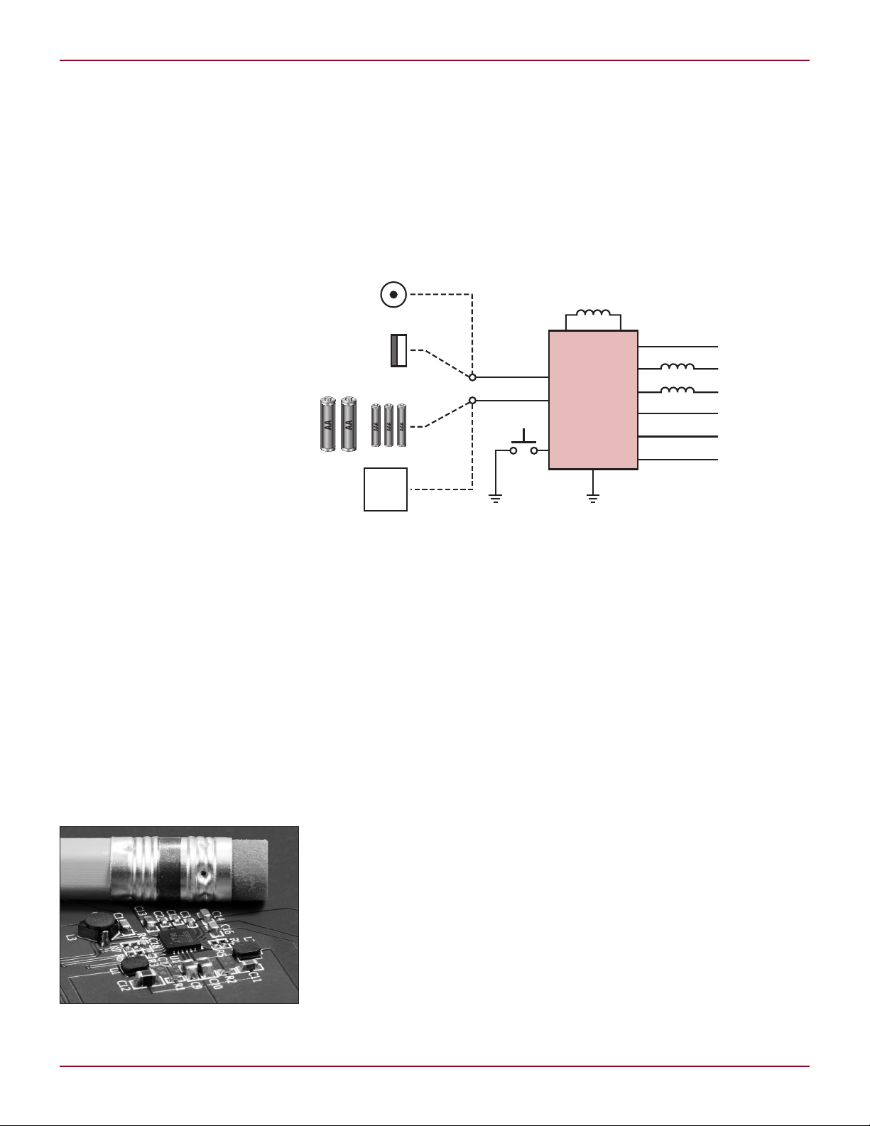
Power Management IC with
Pushbutton Control Generates Six
Voltage Rails from USB or 2 AA Cells
Via Low Loss PowerPath Topology
Introduction
As the complexity of portable electronic
devices continues to increase, the demands placed on power supplies, and
their designers, expand dramatically.
Not only must typical power systems
accommodate multiple input sources,
with voltages as low as 1.8V for two
AA cells, but they must also provide
an increasing number of independent
output rails to support a wide range
of requirements—for memory, microprocessors, backlights, audio and RF
components. To further complicate
matters, expanding feature sets add up
to increased power dissipation, making
it important to optimize overall power
system efficiency. This is particularly
challenging given that the constant
drive to minimize the required board
area and profile height of the power
system is at direct odds with improving efficiency.
The LTC3101 addresses all of these
challenges with a single-IC power
management solution that allows a
designer to easily maximize overall
power system efficiency while minimizing space requirements. The LTC3101
can generate six power rails by integrating three synchronous switching
converters, two protected switched
Figure 2. Complete portable power
solution with a 16mm × 19mm footprint
12
by John Canfield
Figure 1. Six output rails, a low loss PowerPath and integrated pushbutton control
power outputs, and an LDO. Its integrated low loss PowerPath™ topology
allows each switching converter to
run directly from either of two input
power sources.
Two 350mA, high efficiency low
voltage rails, typically used to power
processors and memory, are generated
by synchronous buck converters. Each
converter is able to operate down to an
input voltage of 1.8V thereby enabling
single stage conversion from any input
power source.
A single inductor buck-boost
converter generates a high efficiency
intermediate output rail, typically at
3V or 3.3V, and is able to operate from
either input power source and with
input voltages that are above, below,
or even equal to the output regulation
voltage. The buck-boost converter
can supply a 300mA load at 3.3V for
battery voltages down to 1.8V and an
800mA load for input voltages of 3.0V
and greater.
Two always-alive outputs—MAX,
which tracks the higher voltage input
power source and LDO, a fixed 1.8V
output—provide power to critical
functions that must remain powered
under all conditions. An integrated
pushbutton controller with programmable µP reset generator provides
complete ON/OFF control using only
a minimal number of external components while independent enables allow
total power-up sequencing flexibility.
This complete portable power solution
is packaged in a single low profile 24lead 4mm × 4mm QFN package and
the entire power supply, including
all external components, occupies a
PCB area of less than 3cm2 as shown
in Figure 2.
Zero Loss PowerPath
Topology Maximizes
Efficiency
Although rechargeable Li-Ion and
Li-Polymer batteries are the leading
chemistries for powering portable
devices due to their high energy density and long cycle life, many portable
devices continue to be powered by
alkaline and NiMH cells. This allows
indefinite periods of use away from a
Linear Technology Magazine • June 2009
Page 2
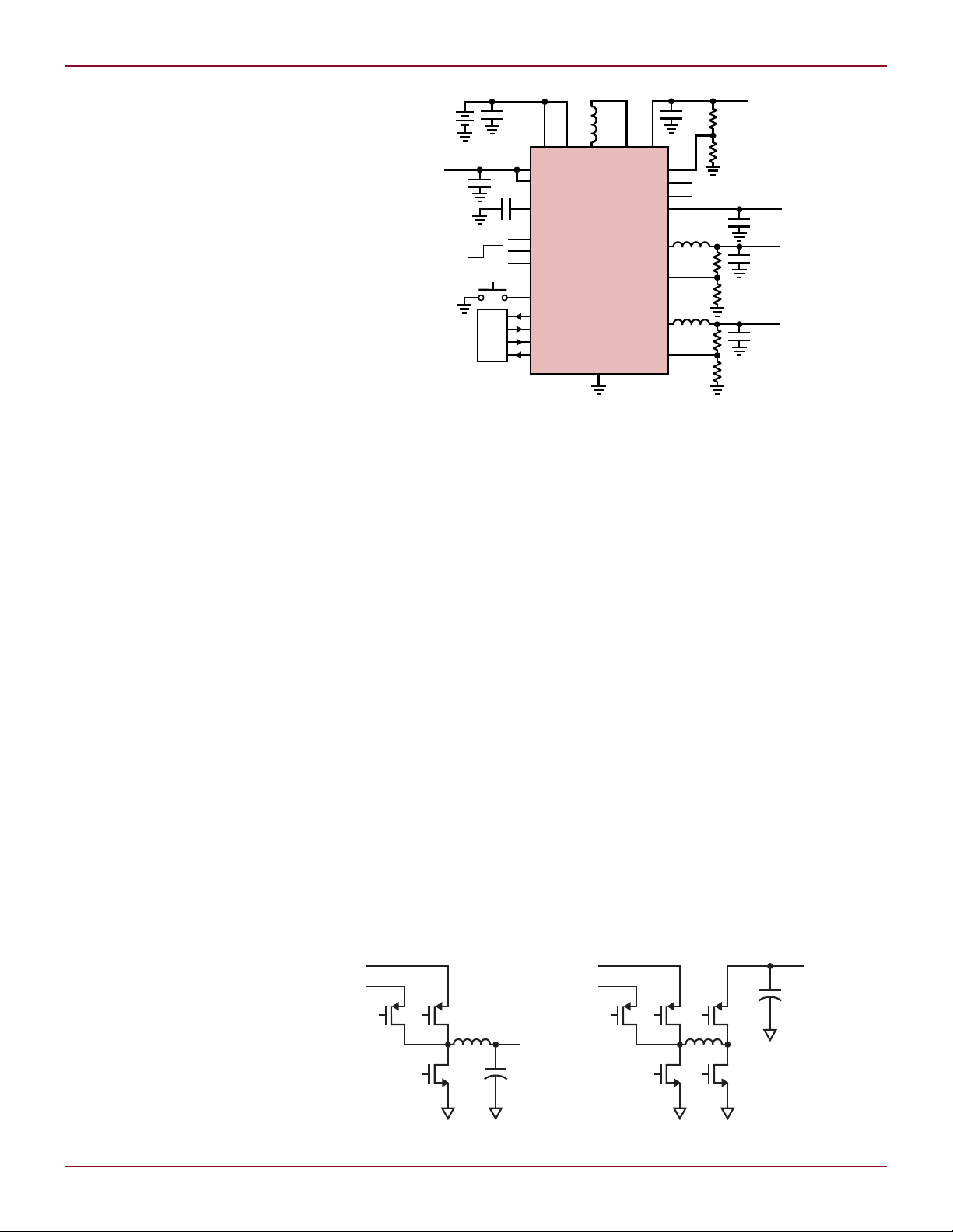
BAT1
USB1
C
RS
ENA1
ENA2
ENA3
PWRKEY
PWRON
PWM
PBSTAT
RESET
USB2
FB3
LDO
SW2
FB2
HSO
MAX
10µF
10µF
2 AA
CELLS
USB/WALL
ADAPTER
1.8V TO 5.5V
10µF
1M
V
OUT3
= 3.3V
300mA FOR VIN ≥ 1.8V
800mA FOR VIN ≥ 3V
221k
Hot Swap OUTPUT: 3.3V AT 100mA
TRACKING OUTPUT: 200mA
4.7µH
4.7µF
1.8V AT 50mA
V
OUT2
1.8V
350mA
V
OUT1
1.5V
350mA
10µF
221k
110k
4.7µH
SW1
FB1
10µF
221k
147k
4.7µH
0.1µF
ON/OFF
BAT2 SW3A
LTC3101
GND
µP
SW3B OUT3
DIS ENA
+
USB
BAT
+
BUCK
V
OUT
USB
BAT
+
BUCK-BOOST
V
OUT
charging socket—which is particularly
important for devices intended for use
in remote locales such as handheld
personal navigation devices or portable
medical devices. Voice recorders, digital still cameras and ultra-small video
recorders are additional examples of
devices that benefit from the ability to
operate from a pair of commonly available batteries, rather than requiring
the lengthy recharging cycle needed
for an internal Li-Ion battery.
Even in portable devices where the
primary power source is restricted
to AA or AAA form factor cells, there
still exist a wide variety of compatible chemistries including alkaline,
rechargeable alkaline, NiMH and
single-use lithium. As a result, the
AA/AAA powered device must accommodate a wide range of input voltages,
from 1.8V for two series alkaline cells
near end of life, to approximately 3.7V
for a pair of fresh non-rechargeable
lithium cells. With its wide 1.8V to
5.5V input voltage range, the LTC3101
can easily support all of these battery chemistries. In addition, the
LTC3101 is able to operate from a
single standard Li-Ion/Polymer cell in
cases where recharging is performed
independently.
Although rechargeable cells are
usually charged outside these types
of devices, the power supply must
accommodate a secondary tethered
power source such as USB or a regulated wall adapter. Consequently, the
power supply must include a means to
generate every power rail from either of
two input sources, and the ubiquitous
3.3V rail must be generated from input
power sources that can be higher or
lower voltage.
In many devices, the capability to
handle dual power sources is provided
by using discrete power MOSFETs to
switch regulator inputs between the
two input power sources or by utilizing
two regulators for generation of each
rail (for example, a buck converter
that generates a 3.3V rail from the
USB input in conjunction with a boost
converter that generates the 3.3V rail
from the battery input).
Both of these approaches suffer
from significant drawbacks. The par-
Linear Technology Magazine • June 2009
allel converter approach increases
system cost and size given that only
one converter is ever active at any given
time and often suffers from glitches
and disruptions to the output rails
during the transition between the
two input power sources. Similarly,
the discrete power switch technique
reduces efficiency due to the addition
of extra series elements in the power
path, increases component count,
and can also lead to disruptions in
the output rails unless the supply
crossover is carefully controlled.
The LTC3101 avoids these problems by using a low loss PowerPath
topology as shown in Figure 4, where
each converter is able to operate directly from either input power source.
In this architecture, each switching
converter utilizes an additional power
switch, which is connected to the
alternate power input. As a result,
each converter is able to run with
maximum efficiency from either input
power source so no efficiency penalty
DESIGN FEATURES L
Figure 3. Typical application
is incurred in supporting dual input
power sources.
The total solution area is minimized
by the fact that the same inductor is
used in either case. In addition, the
automatic transition between the
two input power sources is seamless—there is no interruption to any
of the output rails. Figure 5 shows the
transient response of the buck-boost
converter as the input power source
transitions from battery power to USB
power in response to a live cable plug
into a USB port.
Integrated Buck-Boost
Provides High Efficiency
3V/3.3V Rail from
Any Power Source
In many portable devices an intermediate supply rail, typically regulated to
3.3V, is required to power an RF stage
or audio amplifiers. Often this rail is
generated from the two series AA cells
using a boost converter. However, the
higher cell voltage of single-use lithium
Figure 4. The low loss PowerPath architecture
13
Page 3

L DESIGN FEATURES
OUTPUT
VOLTAGE
200mV/DIV
INDUCTOR
CURRENT
200mA/DIV
V
USB
2V/DIV
100µs/DIV
batteries such as the Energizer e2
brand can cause problems when the
battery voltage is significantly higher
than the output voltage. Depending
on the boost converter utilized, this
can result in low efficiency operation
or even loss of regulation on the 3.3V
rail.
To avoid this problem, the LTC3101
generates the 3.3V rail utilizing a
buck-boost converter, which accepts
any input voltage in the range 1.8V to
5.5V without sacrificing efficiency. In
fact, when operating with a fresh pair
of single-use lithium batteries at 3.7V,
the LTC3101 buck-boost efficiency is
greater than 94% at 150mA load current. In addition, the same buck-boost
converter is able to operate directly
from the USB input, so generation
of the 3.3V rail requires only a single
inductor.
Reverse Blocking LDO
Enables Data Retention
During Battery Swaps
Many portable electronic devices contain critical circuitry such as real time
clocks, which must remain powered
under all conditions. The MAX and
LDO outputs of the LTC3101 are alive
as long as either input power source
is present, regardless of the state of
the pushbutton interface or enable
inputs. It is also possible to connect
a large capacitor directly to the LDO
output to serve as a charge reservoir
for powering critical functions during
times, such as battery swaps, when
both input power sources are temporarily removed. In its reverse blocking
state, the maximum reverse current
through the LDO is limited to under
1µA in order to preserve charge in the
reservoir capacitor.
Figure 5. Buck-boost output voltage transient on USB hot plug
14
MAX and Hot Swap Outputs
Power Additional Regulators
and Flash Memory Cards
Portable electronic devices often require additional miscellaneous power
supplies, such as current regulated
drivers for LED backlighting and LDOs
for low power rails. Typically these
secondary supplies must be functional
whenever either input power source
is present, so they also require power
path control to switch between the two
input power sources.
External supplies can take advantage of the LTC3101’s PowerPath
control circuit via the MAX output,
which continuously tracks the higher
voltage input power source. Additional
regulators can be directly connected
to this output, thus freeing the designer from the need to implement
an additional switched power path.
The MAX output is able to support a
200mA load and is current limited to
protect against overload conditions
and short circuits.
Many portable electronic devices
provide flash memory card interfaces for use as bulk storage memory.
Typical flash memory cards such as
Compact Flash (CF) and Secure Digital (SD) formats require a regulated
3.3V supply that is typically capable
of providing tens of milliamps. However, many flash memory cards have
a significant amount of supply bypass
capacitance installed on the card and
when hot plugged into a live 3.3V rail,
the inrush current required to charge
these supply bypass capacitors on
the memory card can momentarily
drag down the host’s supply, causing disruption to other ICs powered
by that rail.
The LTC3101’s dedicated 100mA
hot swap output (powered from the
buck-boost converter rail) does not
have this problem. The independent
current limit of the hot swap switch
allows flash memory cards to be hot
plugged without disruption to the
primary 3.3V rail. In addition, the
hot swap output is fully short circuit
protected to safeguard against accidental shorts at the memory card
interface port.
Low Quiescent Current
Minimizes Battery Drain
Most portable electronic devices spend
significant, if not the majority, of their
time in sleep or standby modes. In fact,
even when an appliance is off, there is
often circuitry that must remain powered, including real time clocks and
volatile memory storing configuration
settings. The always-alive 1.8V LDO
and tracking MAX outputs remain
powered whenever either input power
source is present allowing them to be
utilized for supplying such critical
functions. In order to minimize battery
discharge during this time, the total
quiescent current draw of the LTC3101
with both the MAX and LDO outputs
active is reduced to 15µA.
Many portable electronic devices
also support a standby mode in which
several of the system’s voltage rails
must be kept in regulation. Typically,
in standby the microprocessor and
memory remain powered and the
processor is placed in a low current
sleep mode enabling the device to return to an active operating state with
minimal delay.
In order to minimize battery drain
in such modes of operation, all three
switching converters in the LTC3101
feature Burst Mode operation, which
can be enabled via a dedicated pin.
With Burst Mode operation enabled,
the buck converters automatically
transition from PWM to Burst Mode
operation at sufficiently light load
(typically 10mA) while the buck-boost
converter uses Burst Mode operation
at all load currents. In Burst Mode
operation with all six output rails
maintained in regulation the total
quiescent current draw of the LTC3101
Linear Technology Magazine • June 2009
Page 4

is reduced to only 38µA. In addition,
HSO
(OPTIONAL)
ENA1
ENA2
R
FILT
C
FILT
500µs/DIV
V
OUT
BUCK 1
(1V/DIV)
V
OUT
BUCK 2
(1V/DIV)
V
OUT
BUCK-BOOST
(2V/DIV)
HOT SWAP
(2V/DIV)
500µs/DIV
V
OUT
BUCK 1
(1V/DIV)
V
OUT
BUCK 2
(1V/DIV)
V
OUT
BUCK-BOOST
(2V/DIV)
HOT SWAP
(2V/DIV)
to ensure low supply rail noise, the
Burst Mode operation output voltage
ripple is typically less than 1% of the
regulation voltage of each output rail.
All three switching converters can be
forced into fixed frequency PWM mode
operation to ensure low noise operation while critical system functions
are underway.
DESIGN FEATURES L
Figure 6. Default power-up sequencing
Flexible Power-Up
Sequencing Options
The LTC3101 provides a variety of
sequencing options. Most systems
that incorporate multiple power
supply rails require that they come
into regulation in a certain sequence
with specific timing. This is because
individual ICs and modules that are
powered from multiple rails need
particular sequencing to minimize
start-up current and ensure predictable power-up behavior.
Common examples include microprocessors and FPGAs, which often
require that the peripheral supply
powering the I/O buffers is made
available only after the lower voltage
core is in regulation. In addition, at
the board level, many systems bring
up the supplies for peripheral devices
only after the processor is powered up
to avoid erratic behavior from peripherals lacking processor oversight.
Each switching converter in the
LTC3101 has an internal power-good
comparator, which is used internally
to sense when that rail is in regulation. The default power-up sequence
enables the individual outputs in the
following order: buck converter 1, buck
converter 2, buck-boost converter,
and finally the hot swap output. Each
converter is enabled once the preceding converter in the sequence reaches
regulation (typically 94% of the target
output voltage). The default power-up
sequence using all converter channels
is shown in Figure 6.
If the dedicated enable pin for any
switching converter is held low during
the pushbutton triggered initiation,
that converter is simply skipped in
the default power-up sequence, but
that channel can still be enabled at a
later time. This functionality allows the
LTC3101 to implement any arbitrary
power-up sequence using few if any
external components.
can be accomplished by adding a
simple RC filter with the desired time
constant between the hot swap output
and the buck enables. Notice however,
that if the hot swap output is forced
to ground, the buck converters will
be disabled. If there is a potential for
the hot swap output to fall below the
enable threshold (typically 0.7V) dur ing normal operation, then the buck
enables can instead be driven through
an RC delay from the buck-boost voltage directly rather than from the hot
swap output.
For example, in some systems the
3.3V buck-boost rail must come up
first, followed by both buck rails in
unison. This can be accomplished
by driving the buck enables from the
hot swap output, HSO, as shown in
Figure 7. The bucks do not power up
in the normal sequence since their
enables are low to start. Once the
buck-boost reaches regulation, the hot
swap output is enabled, which in turn
enables the two buck converters. Since
the hot swap output is not powered
until the buck-boost is in regulation,
this configuration ensures that the
buck converters do not become active
until after the buck-boost is in regulation, as shown by the waveforms in
Figure 8.
If an additional delay is required
Conclusion
The LTC3101 is perfectly suited for
the needs of the next generation of
extended functionality compact portable electronic devices.
The job of the power system designer
is simplified by its compact solution
footprint and ability to generate six
commonly required output voltage
rails automatically from two independent wide input voltage range power
sources. The LTC3101’s low quiescent
current and a high efficiency, low loss
PowerPath architecture maximize
battery life. A wide range of output
voltages, programmable duration
µP reset generator, and independent
enables offer flexibility and easy customization.
before the bucks are enabled, this
L
Figure 7. Sequencing the buck enables
using the hot swap output rail
Linear Technology Magazine • June 2009
Figure 8. Power-up sequencing, buck-boost followed by the buck outputs
15
 Loading...