

Page 1
1.5A Single Resistor
Rugged Linear Regulator
FeaTures DescripTion
LT3081
with Monitors
n
Extended Safe Operating Area
n
Maximum Output Current: 1.5A
n
Stable with or without Input/Output Capacitors
n
Wide Input Voltage Range: 1.2V to 36V
n
Single Resistor Sets Output Voltage
n
Output Current Monitor: I
n
Junction Temperature Monitor: 1µA/°C
n
Output Adjustable to 0V
n
50µA SET Pin Current: 1% Initial Accuracy
n
Output Voltage Noise: 27µV
n
Parallel Multiple Devices for Higher Current or
MON
= I
RMS
OUT
/5000
Heat Spreading
n
Programmable Current Limit
n
Reverse-Battery and Reverse-Current Protection
n
<1mV Load Regulation Typical Independent of V
n
<0.001%/V Line Regulation Typical
n
Available in Thermally-Enhanced 12-Lead 4mm × 4mm
OUT
DFN and 16-Lead TSSOP, 7-Lead DD-Pak and 7-Lead
TO-220
applicaTions
n
All Surface Mount Power Supply
n
Rugged Industrial Power Supply
n
Post Regulator for Switching Supplies
n
Low Output Voltage Supply
n
Intrinsic Safety Applications
The LT®3081 is a 1.5A low dropout linear regulator de-
signed for rugged industrial applications. Key features of
the IC are the extended safe operating area (SOA), output
current monitor, temperature monitor and programmable
current limit. The LT3081 can be paralleled for higher
output current or heat spreading. The device withstands
reverse input and reverse output-to-input voltages without
reverse current flow.
The LT3081’s precision 50µA reference current source
allows a single resistor to program output voltage to
any level between zero and 34.5V. The current reference
architecture makes load regulation independent of output
voltage. The LT3081 is stable with or without input and
output capacitors.
The output current monitor (I
/5000) and die junction
OUT
temperature output (1µA/°C) provide system monitoring
and debug capability. In addition, a single resistor programs current limit.
Internal protection circuitry includes reverse-battery and
reverse-current protection, current limiting and thermal
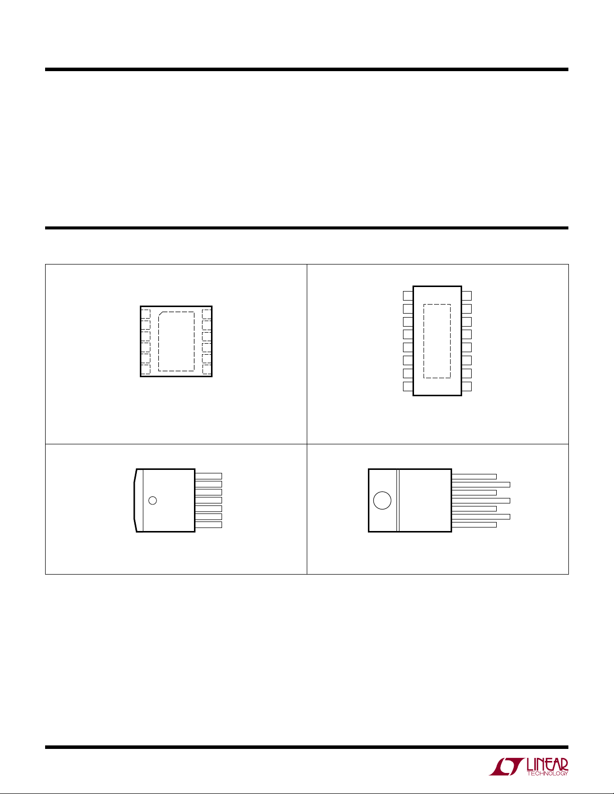
limiting. The LT3081 is offered in the 16-lead TSSOP (with
exposed pad for improved thermal performance), 7-lead
TO-220, 7-lead DD-Pak, and an 12-lead 4mm × 4mm DFN.
L, LT, LTC, LTM, Linear Technology and the Linear logo are registered trademarks of Linear
Technology Corporation. All other trademarks are the property of their respective owners.
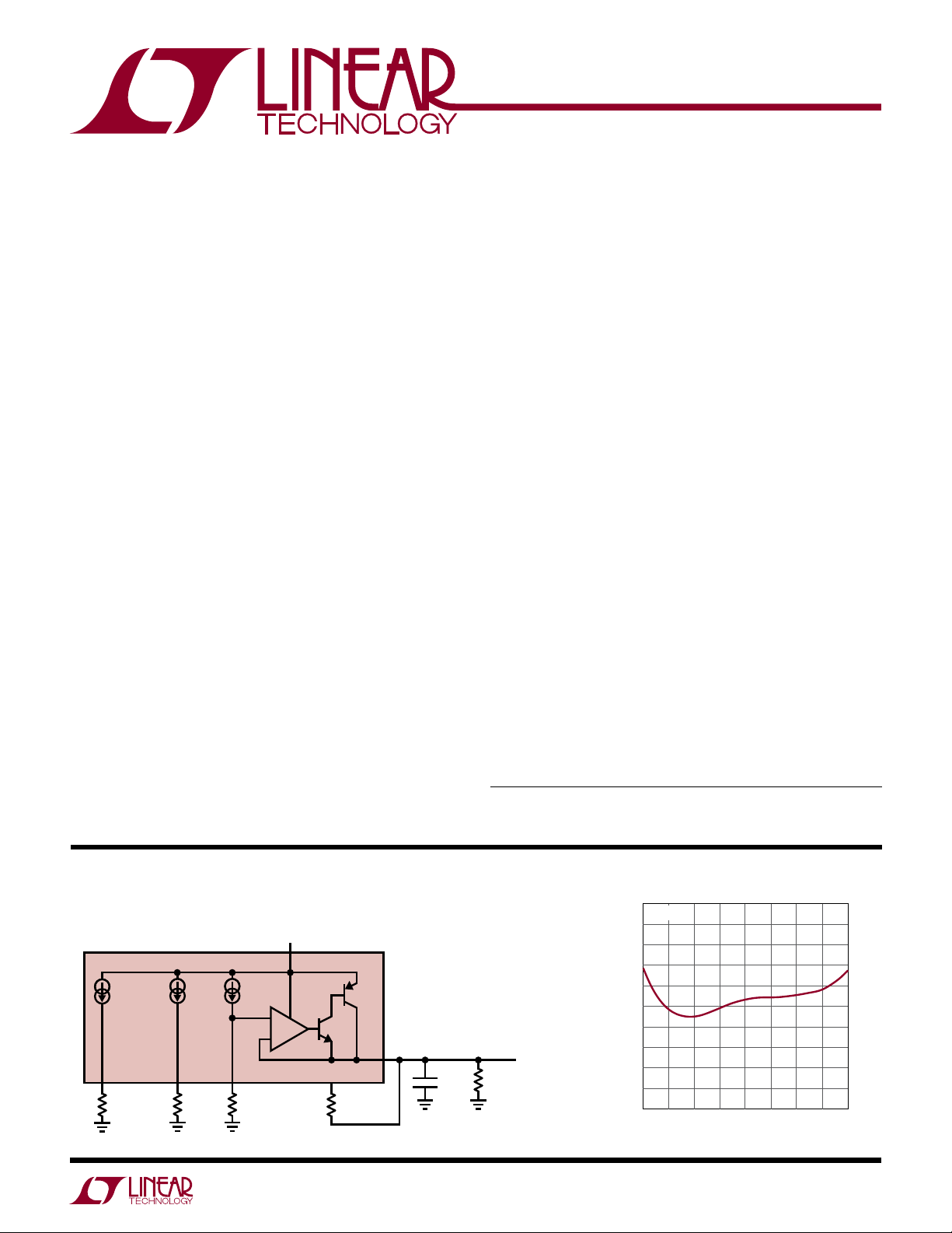
Typical applicaTion
Wide Safe Operating Area Supply
V
IN
LT3081
I
I
MON
1k
LOAD
/5000
1µA/°C
TEMP
1k
50µA
SET
30.1k
IN
+
–
OUT
I
LIM
4.53k
For more information www.linear.com/LT3081
10µF*
*OPTIONAL
300Ω*
3081 TA01a
I
OUT
1.5V
1A
SET Pin Current
50.5
IL = 5mA
50.4
50.3
50.2
50.1
50.0
49.9
49.8
SET PIN CURRENT (µA)
49.7
49.6
49.5
–50
–25 25
0
TEMPERATURE (°C)
125
50
100
75
3081 TA01b
150
3081fc
1
Page 2
LT3081
TOP VIEW
12-LEAD (4mm × 4mm) PLASTIC DFN
TEMP
16-LEAD PLASTIC TSSOP
TOP VIEW
OUT
OUT
OUT
OUT
OUT
I
OUT
TEMP
7-LEAD PLASTIC DD
FRONT VIEW
TAB IS
TEMP
7-LEAD PLASTIC TO-220
TAB IS
TEMP
FRONT VIEW
absoluTe MaxiMuM raTings
(Note 1) All Voltages Relative to V
IN Pin to OUT Pin Differential Voltage .....................±40V
SET Pin Current (Note 6) .....................................±25mA
SET Pin Voltage (Relative to OUT, Note 6) .............. ±10V
TEMP Pin Voltage (Relative to OUT) ................. 1V, –40V
Pin Voltage (Relative to OUT) .........................±0.2V
I
LIM
Pin Voltage (Relative to OUT) ................... 1V, –40V
I
MON
Output Short-Circuit Duration .......................... Indefinite
pin conFiguraTion
1
OUT
2
OUT
3
OUT
OUT
I
LIM
SET
= 125°C, θJA = 32°C/W, θJC = 4°C/W
T
JMAX
EXPOSED PAD (PIN 13) IS OUT, MUST BE SOLDERED TO PCB
4
5
6
13
OUT
DF PACKAGE
IN
12
IN
11
IN
10
IN
9
8
7
I
MON
.
OUT
Operating Junction Temperature Range (Note 2)
E-, I-Grades ....................................... –40°C to 125°C
H-Grade ............................................. –40°C to 150°C
MP-Grade .......................................... –55°C to 150°C
Storage Temperature Range .................. –65°C to 150°C
Lead Temperature (Soldering, 10 sec)
FE, R, T7 Packages Only ................................... 300°C
1
2
3
4
17
OUT
5
6
LIM
7
SET
8
FE PACKAGE
= 150°C, θJA = 29°C/W, θJC = 8°C/W
T
JMAX
EXPOSED PAD (PIN 17) IS OUT, MUST BE SOLDERED TO PCB
OUT
16
IN
15
IN
14
IN
13
IN
12
11
I
10
MON
OUT
9
2
OUT
R PACKAGE
= 125°C, θJA = 15°C/W, θJC = 3°C/W
T
JMAX
7
6
5
4
3
2
1
NC
IN
OUT
I
MON
SET
I
LIM
7
6
5
OUT
= 150°C, θJA = 40°C/W, θJC = 3°C/W
T
JMAX
4
3
2
1
T7 PACKAGE
NC
IN
OUT
I
MON
SET
I
LIM
3081fc
For more information www.linear.com/LT3081
Page 3
LT3081
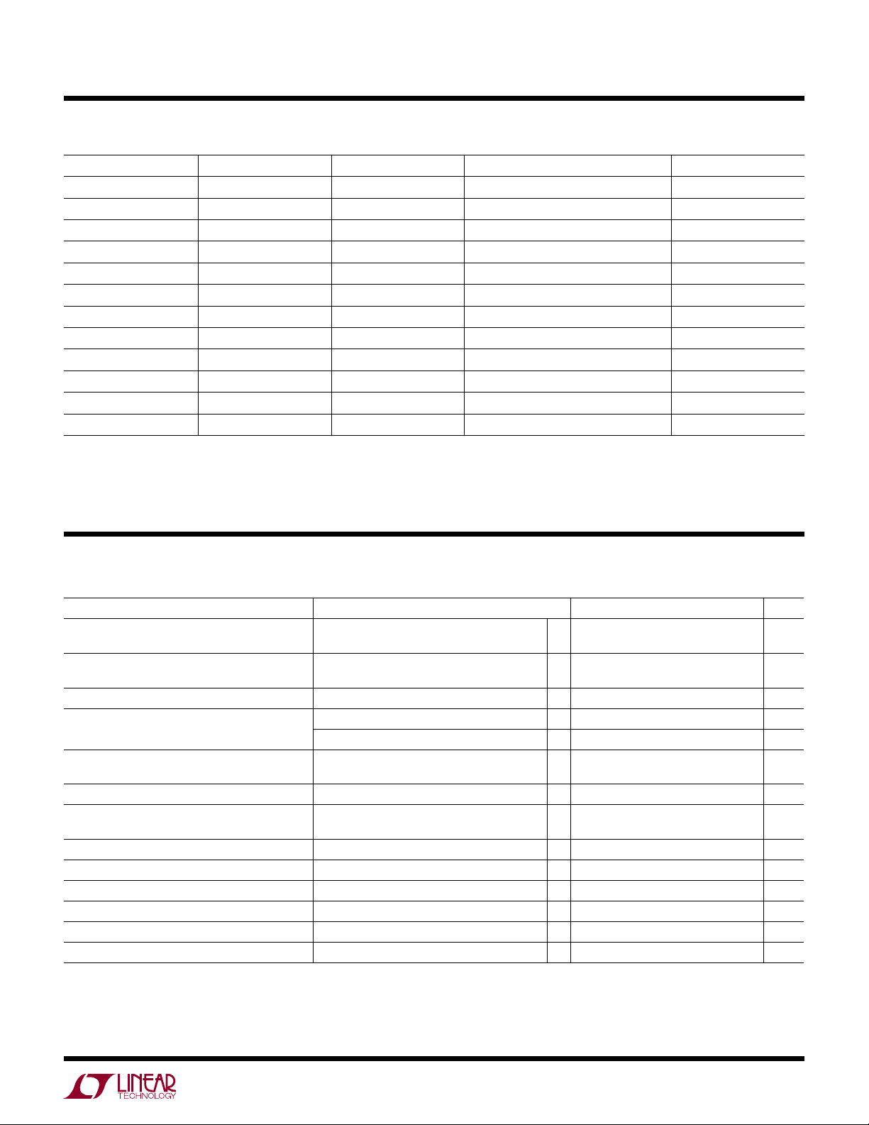
orDer inForMaTion
LEAD FREE FINISH TAPE AND REEL PART MARKING* PACKAGE DESCRIPTION TEMPERATURE RANGE
LT3081EDF#PBF LT3081EDF#TRPBF 3081
LT3081IDF#PBF LT3081IDF#TRPBF 3081
12-Lead (4mm × 4mm) Plastic DFN
12-Lead (4mm × 4mm) Plastic DFN
LT3081EFE#PBF LT3081EFE#TRPBF 3081FE 16-Lead Plastic TSSOP –40°C to 125°C
LT3081IFE#PBF LT3081IFE#TRPBF 3081FE 16-Lead Plastic TSSOP –40°C to 125°C
LT3081HFE#PBF LT3081HFE#TRPBF 3081FE 16-Lead Plastic TSSOP –40°C to 150°C
LT3081MPFE#PBF LT3081MPFE#TRPBF 3081FE 16-Lead Plastic TSSOP –55°C to 150°C
LT3081ER#PBF LT3081ER#TRPBF LT3081R 7-Lead Plastic DD-Pak –40°C to 125°C
LT3081IR#PBF LT3081IR#TRPBF LT3081R 7-Lead Plastic DD-Pak –40°C to 125°C
LT3081ET7#PBF NA LT3081T7 7-Lead Plastic TO-220 –40°C to 125°C
LT3081IT7#PBF NA LT3081T7 7-Lead Plastic TO-220 –40°C to 125°C
LT3081HT7#PBF NA LT3081T7 7-Lead Plastic TO-220 –40°C to 150°C
LT3081MPT7#PBF NA LT3081T7 7-Lead Plastic TO-220 –55°C to 150°C
Consult LTC Marketing for parts specified with wider operating temperature ranges. *The temperature grade is identified by a label on the shipping container.
Consult LTC Marketing for information on nonstandard lead based finish parts.
For more information on lead free
part marking, go to: http://www.linear.com/leadfree/
For more information on tape and reel specifications, go to: http://www.linear.com/tapeandreel/
–40°C to 125°C
–40°C to 125°C
elecTrical characTerisTics
The l denotes the specifications which apply over the full operating
temperature range, otherwise specifications are at TJ = 25°C. (Note 2)
PARAMETER CONDITIONS MIN TYP MAX UNITS
SET Pin Current I
SETVIN
= 2V, I
2V ≤ V
Offset V
oltage V
(V
– V
SET
)
= 5mA to 1.5A
LOAD
OUT
Load Regulation ∆I
I
SET
Load Regulation ∆I
V
OS
(Note 7)
Line Regulation ∆I
∆V
OS
SET
OS
= 2V, I
V
IN
V
= 2V, I
IN
LOAD
DF, FE Packages
R, T7 Packages
∆VIN = 2V to 36V, I
∆V
= 2V to 36V, I
IN
Minimum Load Current (Note 3) 2V ≤ V
Dropout Voltage (Note 4) I
Internal Current Limit V
Programming Ratio
I
LIM
Minimum Output Current Resistance 450 Ω
I
LIM
Full-Scale Output Current I
I
MON
Scale Factor 100mA ≤ I
I
MON
Operating Range
I
MON
= 100mA
LOAD
I
= 1.5A
LOAD
= 5V, V
IN
= 1.5A 290 300 330 µA
LOAD
= 5mA
LOAD
≤ 36V, 5mA ≤ I
IN
= 5mA
LOAD
= 5mA
LOAD
LOAD
≤ 1.5A
= 5mA to 1.5A –0.1 nA
= 5mA
LOAD
= 5mA
LOAD
≤ 36V
IN
= 0V, V
SET
≤ 1.5A 200 µA/A
LOAD
OUT
= –0.1V
49.5
l
48.75
–1.5
l
–3.5
l
l
50
50
0
0
–0.5 –3 mV
–1.5 –4 mV
1.5
0.001
l
l
l
1.5 2 A
l
300 360 500 mA/kΩ
l
V
– 40V V
OUT
1.1 5 mA
1.21
1.23
OUT
50.5
51.25
1.5
3.5
mV/V
1.5
+ 0.4V V
µA
µA
mV
mV
nA/V
V
V
For more information www.linear.com/LT3081
3081fc
3
Page 4
LT3081
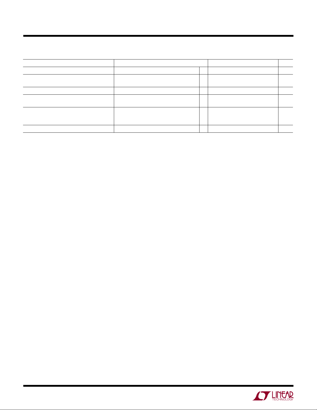
elecTrical characTerisTics
The l denotes the specifications which apply over the full operating
temperature range, otherwise specifications are at TJ = 25°C. (Note 2)
PARAMETER CONDITIONS MIN TYP MAX UNITS
TEMP Output Current (Note 9) T
TEMP Output Current Absolute Error (Note 9) 0°C <T
Reference Current RMS Output Noise (Note 5) 10Hz ≤ f ≤ 100kHz 5.7 nA
Error Amplifier RMS Output Noise (Note 5) I
Ripple Rejection
V
= 0.5V
RIPPLE
C
=10µF, VIN = V
OUT
Thermal Regulation, I
Note 1: Stresses beyond those listed under Absolute Maximum Ratings
may cause permanent damage to the device. Exposure to any Absolute
Maximum Rating condition for extended periods may affect device
reliability and lifetime.
Note 2: Unless otherwise specified, all voltages are with respect to V
The LT3081 is tested and specified under pulse load conditions such
that T
≈ TA. The LT3081E is tested at TA = 25°C and performance is
J
guaranteed from 0°C to 125°C. Performance of the LT3081E over the
full –40°C and 125°C operating temperature range is assured by design,
characterization, and correlation with statistical process controls. The
LT3081I is guaranteed over the full –40°C to 125°C operating junction
temperature range. The LT3081MP is 100% tested and guaranteed
over the –55°C to 150°C operating junction temperature range. The
LT3081H is tested at 150°C operating junction temperature. High junction
temperatures degrade operating lifetimes. Operating lifetime is degraded at
junction temperatures greater than 125°C.
Note 3: Minimum load current is equivalent to the quiescent current of
the part. Since all quiescent and drive
of the part, the minimum load current is the minimum current required to
maintain regulation.
, I
P-P
LOAD
OUT(NOMINAL)
= 0.1A, C
SET
= 0.1µF,
SET
+ 3V
current is delivered to the output
> 5°C 1 µA/°C
J
≤ 125°C
J
125°C <T
LOAD
C
SET
f = 120Hz
f = 10kHz
f = 1MHz
10ms Pulse 0.003 %/W
≤ 150°C
J
= 1.5A, 10Hz ≤ f ≤ 100kHz, C
= 0.1µF
Note 4:
output voltage differential required supplying a given output current.
Note 5: Adding a small capacitor across the reference current resistor
lowers output noise. Adding this capacitor bypasses the resistor shot
noise and reference current noise; output noise is then equal to error
.
OUT
amplifier noise (see Applications Information section).
Note 6: Diodes with series 400Ω resistors clamp the SET pin to the
OUT pin. These diodes and resistors only carry current under transient
overloads.
Note 7: Load regulation is Kelvin sensed at the package.
Note 8: This IC includes overtemperature protection that protects the
device during momentary overload conditions. Junction temperature
exceeds the maximum operating junction temperature when
overtemperature protection is active. Continuous operation above the
specified maximum operating junction temperature may impair device
reliability.
Note 9: The TEMP pin output current represents the average die junction
temperature. Due to power dissipation and thermal gradients across the
die, the TEMP pin output current measurement does not guarantee that
absolute maximum junction temperature is not exceeded.
=10µF,
OUT
For the LT3081, dropout is specified as the minimum input-to-
–10
–15
75 90
10
15
27 µV
75
20
µA
µA
RMS
RMS
dB
dB
dB
4
3081fc
For more information www.linear.com/LT3081
Page 5
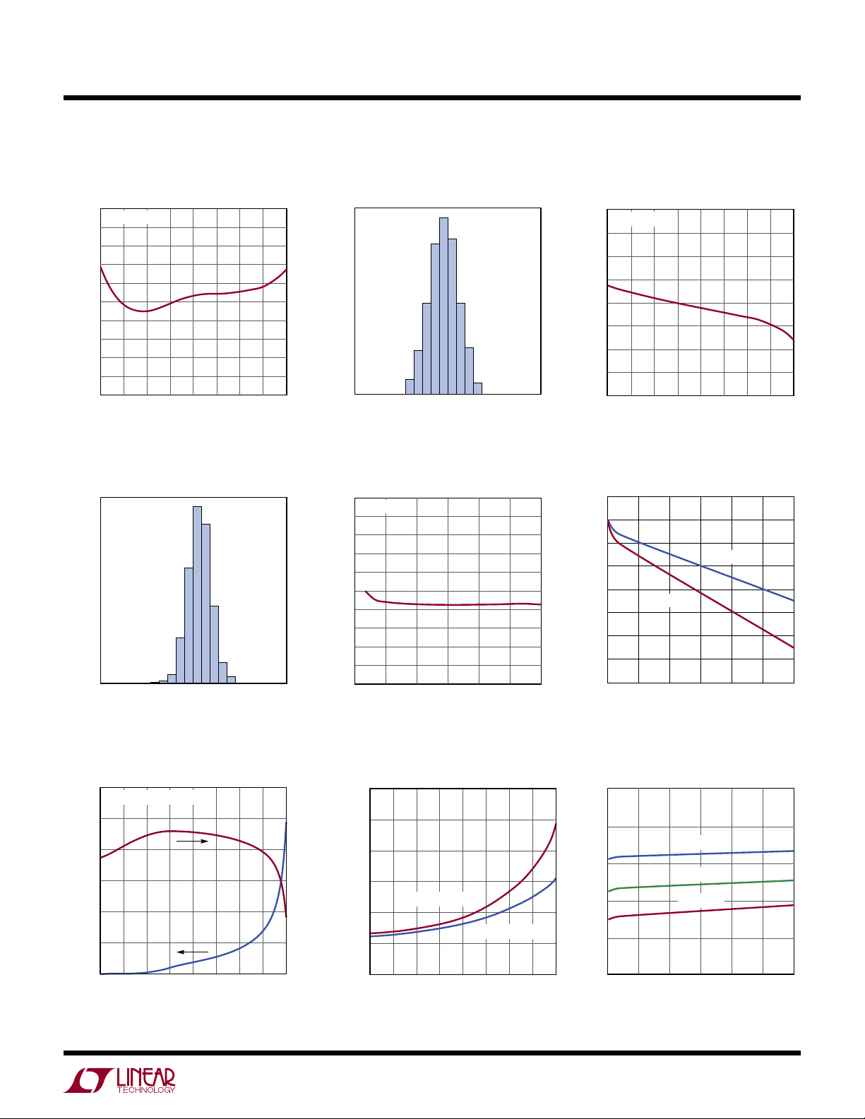
Typical perForMance characTerisTics
3081 G01
3081 G05
3081 G07
3081 G09
= 25°C unless otherwise specified.
T
J
LT3081
SET Pin Current SET Pin Current
50.5
I
= 5mA
LOAD
50.4
50.3
50.2
50.1
50.0
49.9
49.8
SET PIN CURRENT (µA)
49.7
49.6
49.5
–50
–25 25
0
TEMPERATURE (°C)
Offset Voltage
N = 3195
–2
–1 0
VOS DISTRIBUTION (mV)
75
100
1 2
3081 G04
150
50
125
N = 3195
49
SET PIN CURRENT DISTRIBUTION (µA)
Offset Voltage (V
1.0
I
LOAD
0.8
0.6
0.4
0.2
0
–0.2
–0.4
OFFSET VOLTAGE (mV)
–0.6
–0.8
–1.0
0
INPUT-TO-OUTPUT DIFFERENTIAL (V)
49.5 50
= 5mA
6
12
– V
OUT
18 24
Offset Voltage (V
2.0
I
= 5mA
LOAD
1.5
1.0
0.5
0
–0.5
OFFSET VOLTAGE (mV)
–1.0
–1.5
50.5 51
3081 G02
) Offset Voltage (V
SET
36
30
–2.0
–25
–50
0.2
0
–0.2
–0.4
–0.6
–0.8
OFFSET VOLTAGE (mV)
–1.0
–1.2
–1.4
0
0
TJ = 125°C
0.25
– V
OUT
50
25
TEMPERATURE (°C)
0.5 1
LOAD CURRENT (A)
75
– V
OUT
TJ = 25°C
0.75 1.25
SET
100
SET
)
150
125
3081 G03
)
1.5
3081 G06
Load Regulation Minimum Load Current Dropout Voltage
300
∆I
= 5mA TO 1.5A
LOAD
250
200
150
100
50
SET PIN CURRENT LOAD REGULATION (nA)
0
–50
0 50
–25 25
TEMPERATURE (°C)
100
75
125
150
0
–0.5
–1.0
–1.5
–2.0
–2.5
–3.0
3.0
OFFSET VOLTAGE LOAD REGULATION (mV)
2.5
2.0
1.5
1.0
MINIMUM LOAD CURRENT (mA)
0.5
0
–25 25
–50
For more information www.linear.com/LT3081
VIN – V
= 36V
OUT
0 50
TEMPERATURE (°C)
VIN – V
75
OUT
100
= 2V
125
3081 G08
1.5
1.4
1.3
1.2
DROPOUT VOLTAGE (V)
1.1
1.0
150
0
0.25
TJ = –50°C
TJ = 25°C
TJ = 125°C
0.5 0.75 1
LOAD CURRENT (A)
1.25 1.5
3081fc
5
Page 6
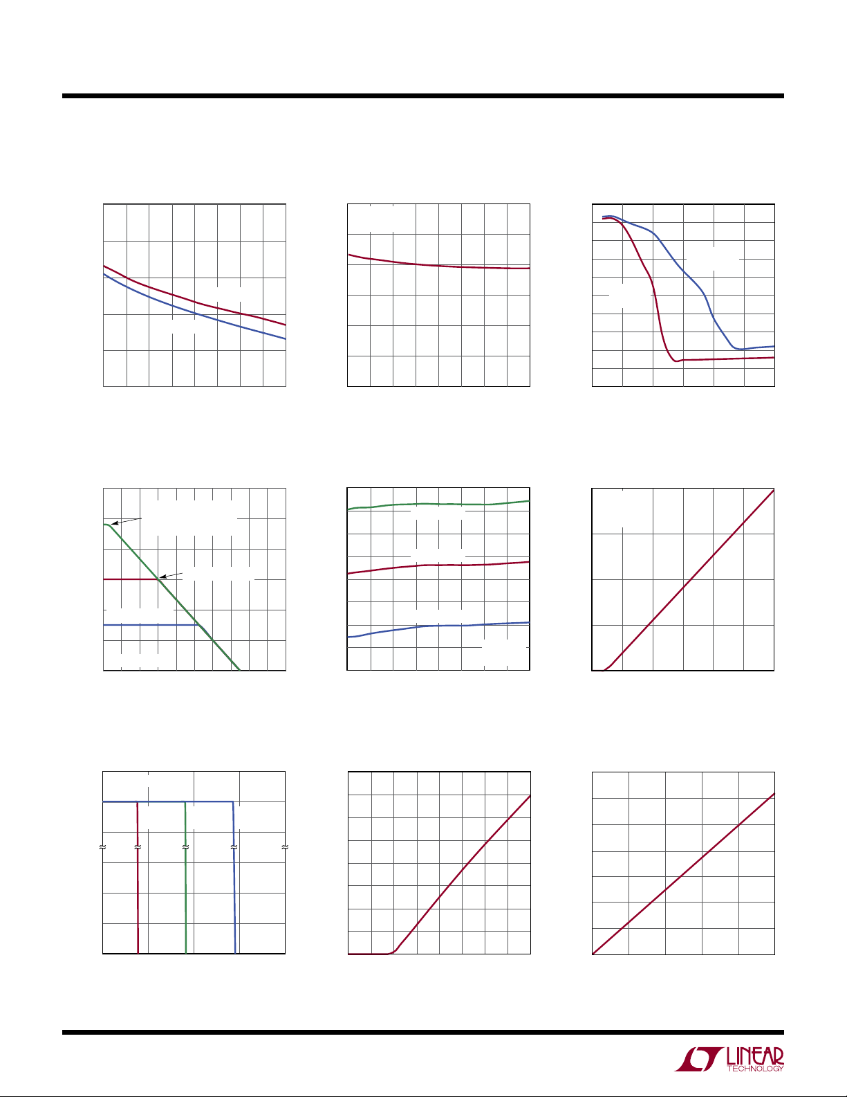
LT3081
3081 G12
3081 G17
Typical perForMance characTerisTics
TJ = 25°C unless otherwise specified.
Dropout Voltage Internal Current Limit Internal Current Limit
1.5
1.4
1.3
1.2
DROPOUT VOLTAGE (V)
1.1
1.0
–50
I
–25 0
TEMPERATURE (°C)
I
= 1.5A
LOAD
= 5mA
LOAD
50
25 75 150
100
125
3081 G10
3.0
VIN = 7V
= 0V
V
OUT
2.5
2.0
1.5
1.0
CURRENT LIMIT (A)
0.5
0
–25 25
–50
0 50
TEMPERATURE (°C)
2.0
1.8
1.6
1.4
1.2
1.0
0.8
CURRENT LIMIT (A)
0.6
0.4
0.2
100
75
125
150
3081 G11
TSSOP
AND DFN
0
6
0
INPUT-TO-OUTPUT DIFFERENTIAL VOLTAGE (V)
12
TO-220 Package Maximum Power
Dissipation Programmable Current Limit Programmable Current Limit
30
25
20
15
POWER (W)
10
VIN – V
5
θJC = 3°C/W
0
50
VIN – V
OUT
LIMITED BY FOLDBACK
CURRENT LIMIT
= 5V
OUT
60
90
70
80
CASE TEMPERATURE (°C)
= 20V
VIN – V
100
= 10V
OUT
110
120 130 140
150
3081 G13
1.6
1.4
1.2
1.0
0.8
0.6
0.4
PROGRAMMED CURRENT LIMIT (A)
0.2
0
–25
–50
R
= 4.53k
ILIM
R
= 3.01k
ILIM
R
= 1.50k
ILIM
0
50
25
TEMPERATURE (°C)
2.0
TJ = 25°C
= 7V
V
IN
= 0V
V
OUT
1.5
1.0
0.5
VIN = 7V
= 0V
V
OUT
75
100
125
150
3081 G39
PROGRAMMED CURRENT LIMIT (A)
0
0
1 2 3 4
R
18 24
(kΩ)
ILIM
TO-220 AND
DD-PAK
30
5 6
3081 G14
36
Programmable Current Limit TEMP Pin Current I
1.05
R
SET
1.00
0.95
0.6
0.4
OUTPUT VOLTAGE (V)
0.2
0
0
6
= 20k
R
ILIM
1.5k
0.5 1 1.5 2
R
ILIM
3.01k
OUTPUT CURRENT (A)
R
4.53k
ILIM
3081 G15
160
140
120
100
80
60
TEMP PIN CURRENT (µA)
40
20
0
–50
–25
0
50
25
TEMPERATURE (°C)
75
100
For more information www.linear.com/LT3081
125
3081 G16
150
Pin Current
MON
350
300
250
200
150
PIN CURRENT (µA)
100
MON
I
50
0
0.3 0.6 0.9 1.5
0
1.2
LOAD CURRENT (A)
3081fc
Page 7
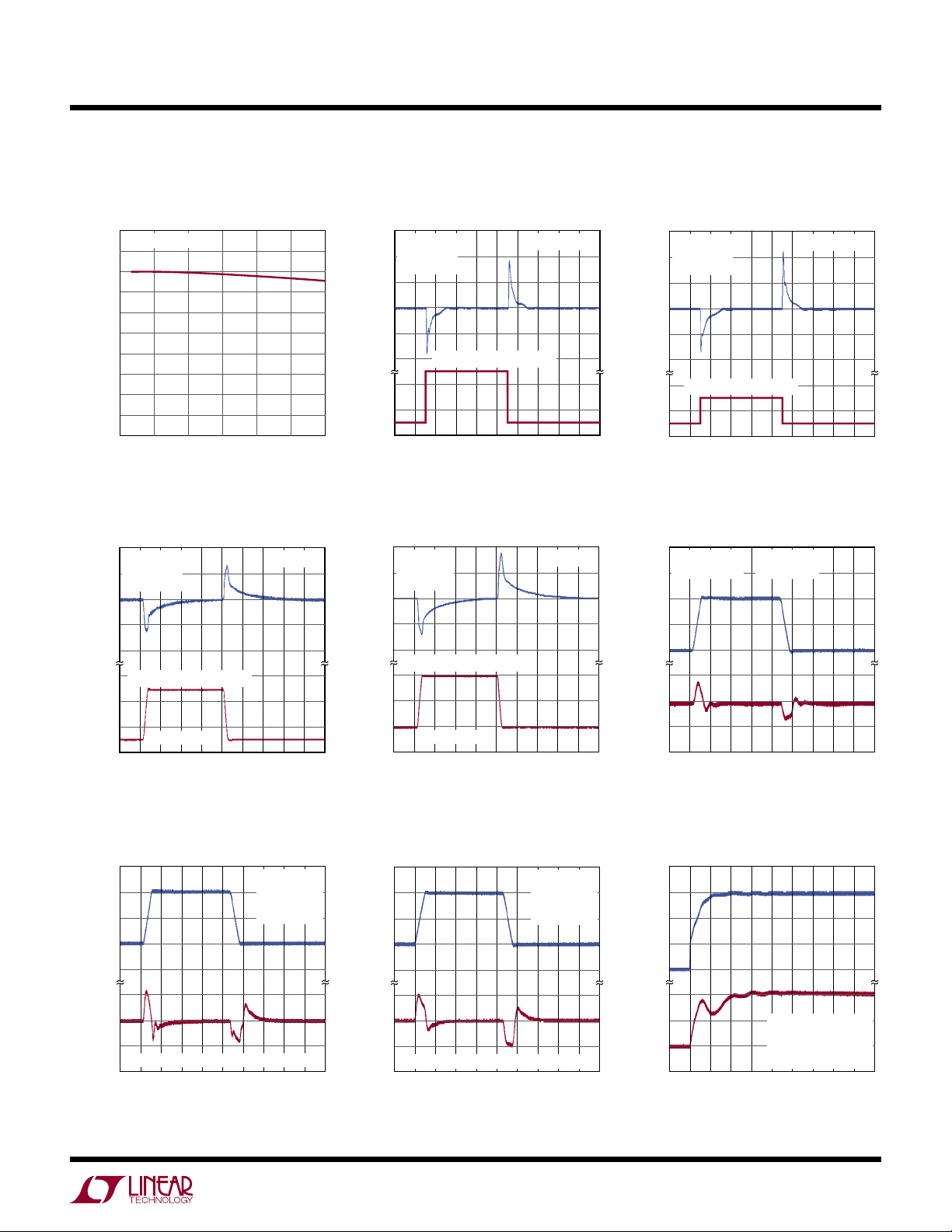
LT3081
3791 TA02b
3081 G20
3081 G22
Typical perForMance characTerisTics
Linear Regulator
I
Pin Line Regulation
MON
50
I
= 200mA
LOAD
45
40
35
30
25
20
PIN CURRENT (µA)
15
MON
I
10
5
0
6
0
INPUT-TO-OUTPUT DIFFERENTIAL VOLTAGE (V)
18 24
12
Linear Regulator
Load Transient Response
200
VIN = 3V
= 1V
V
OUT
100
–100
DEVIATION (mV)
OUTPUT VOLTAGE
–200
600
400
LOAD
200
CURRENT (mA)
= 30pF
C
SET
0
∆I
= 100mA TO 500mA
LOAD
tr = tf = 1µs
0
5 50
0
20
15
25
TIME (µs)
10
36
30
C
= 0
OUT
40 45
30
35
3081 G21
Load Transient Response
150
VIN = 3V
= 1V
V
OUT
100
DEVIATION (mV)
OUTPUT VOLTAGE
–50
–100
400
200
LOAD
CURRENT (mA)
= 0.1µF
C
SET
50
0
∆I
LOAD
0
20 200
0
40
60
Linear Regulator
Load Transient Response
400
VIN = 3V
= 1V
V
OUT
200
–200
DEVIATION (mV)
OUTPUT VOLTAGE
–400
LOAD
CURRENT (mA)
= 30pF
C
SET
0
∆I
= 500mA TO 1.5A
LOAD
1.5
1.0
0.5
0
tr = tf = 1µs
5 50
0
10
15
C
= 100mA TO 500mA
80
100
120
140
TIME (µs)
20
25
30
35
TIME (µs)
TJ = 25°C unless otherwise specified.
Linear Regulator
Load Transient Response
300
= 2.2µF
OUT
160 180
OUTPUT VOLTAGE
LOAD
8081 G19
VIN = 3V
= 1V
V
OUT
200
= 0.1µF
C
SET
100
0
DEVIATION (mV)
–100
–200
2.0
∆I
= 500mA TO 1.5A
LOAD
1.0
0
CURRENT (mA)
20 200
0
40
60
Linear Regulator
Line Transient Response
7
R
C
OUT
40 45
= 0
0.1
–0.1
DEVIATION (mV) INPUT VOLTAGE (V)
OUTPUT VOLTAGE
–0.2
= 20k
SET
= 0.67Ω
R
LOAD
6
5
4
3
0
5 50
0
10
15
80
100
TIME (µs)
C
OUT
C
SET
20
25
TIME (µs)
120
= 2.2µF
= 0.1µF
30
140
35
C
OUT
= 2.2µF
160 180
40 45
3081 G23
Current Source
Line Transient Response
6
5
4
3
2
150
100
50
100mA CURRENT SOURCE CONFIGURATION
0
OUTPUT CURRENT (mA) INPUT VOLTAGE (V)
5 50
0
20
15
25
TIME (µs)
30
10
R
R
C
C
35
SET
OUT
OUT
SET
= 6.04k
= 3.01Ω
= 0
= 30pF
40 45
3081 G24
Current Source
Line Transient Response
6
5
4
3
2
1.2
1.0
0.8
1A CURRENT SOURCE CONFIGURATION
0.6
OUTPUT CURRENT (A) INPUT VOLTAGE (V)
5 50
0
20
10
15
TIME (µs)
For more information www.linear.com/LT3081
R
= 6.04k
SET
= 0.3Ω
R
OUT
= 0
C
OUT
= 30pF
C
SET
25
40 45
30
35
3081 G25
Linear Regulator
Turn-On Response
4
3
2
1
0
1.0
0.5
0
–0.5
OUTPUT VOLTAGE (V) INPUT VOLTAGE (V)
5 50
0
10
15
R
R
C
C
20
25
TIME (µs)
= 20k
SET
= 0.67Ω
LOAD
= 2.2µF CERAMIC
OUT
= 0
SET
30
35
40 45
3081 G26
3081fc
7
Page 8
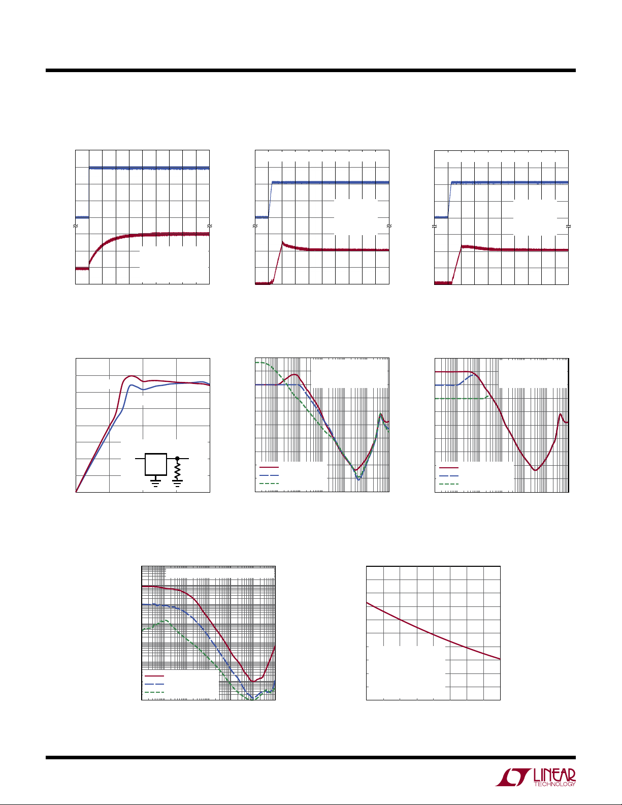
LT3081
3081 G28
3081 G30
3081 G31
Typical perForMance characTerisTics
Linear Regulator
Turn-On Response
4
3
2
1
0
1.0
0.5
0
–0.5
OUTPUT VOLTAGE (V) INPUT VOLTAGE (V)
2 20
0
4
6
R
SET
R
LOAD
C
OUT
C
SET
8
10
TIME (ms)
Residual Output Voltage with
Less Than Minimum Load
800
700
VIN = 36V
600
500
400
300
OUTPUT VOLTAGE (mV)
200
100
0
0
500
VIN = 5V
SET PIN = 0V
V
IN
1000
R
(Ω)
TEST
= 20k
= 0.67Ω
= 2.2µF CERAMIC
= 0.1µF
16 18
12
14
3081 G27
V
R
TEST
1500
OUT
2000
Current Source
Turn-On Response
4
100mA CURRENT SOURCE CONFIGURATION
3
2
1
0
150
100
50
0
20 200
0
OUTPUT CURRENT (mA) INPUT VOLTAGE (V)
80
40
60
100
TIME (µs)
120
R
R
C
C
SET
OUT
OUT
SET
140
= 6.04k
= 3.01Ω
= 0
= 20pF
Ripple Rejection Ripple Rejection
100
90
80
70
60
50
40
30
RIPPLE REJECTION (dB)
20
10
0
I
I
I
10 100
C
= 2.2µF CERAMIC
OUT
= 0.1µF
C
SET
= V
V
IN
OUT(NOMINAL)
= 100mA
LOAD
= 500mA
LOAD
= 1.5A
LOAD
1k 10k 100k 1M 10M
FREQUENCY (Hz)
TJ = 25°C unless otherwise specified.
Current Source
Turn-On Response
4
1A CURRENT SOURCE CONFIGURATION
3
2
1
0
1.5
1.0
0.5
0
160 180
+ 2V
OUTPUT CURRENT (A) INPUT VOLTAGE (V)
20 200
0
40
60
100
90
80
70
60
50
40
30
RIPPLE REJECTION (dB)
20
10
0
10 100
VIN = V
= V
V
IN
= V
V
IN
1k 10k 100k 1M 10M
FREQUENCY (Hz)
80
TIME (µs)
+ 5V
OUT
+ 2V
OUT
+ 1.5V
OUT
R
SET
R
OUT
C
OUT
C
SET
100
120
C
= 2.2µF CERAMIC
OUT
= 0.1µF
C
SET
= 100mA
I
LOAD
= 6.04k
= 0.3Ω
= 0
= 20pF
140
160 180
3081 G29
3081 G32
8
Output Impedance Ripple Rejection (120Hz)
10M
1M
100k
10k
1k
100
OUTPUT IMPEDANCE (Ω)
10
1
CURRENT SOURCE CONFIGURATION
I
SOURCE
I
SOURCE
I
SOURCE
100 1k 10k 100k 1M 10M
10
FREQUENCY (Hz)
= 10mA
= 100mA
= 1A
3081 G33
For more information www.linear.com/LT3081
90
88
86
84
82
80
78
VIN = V
OUT(NOMINAL)
RIPPLE = 500mV
76
RIPPLE REJECTION (dB)
f = 120Hz
74
= 0.1A
I
LOAD
= 2.2µF
C
OUT
72
= 0.1µF
C
SET
70
–50
–25 25
0
TEMPERATURE (°C)
P-P
+ 2V
50
125
100
75
150
3081 G34
3081fc
Page 9
LT3081
3081 G34
3981 G37
Typical perForMance characTerisTics
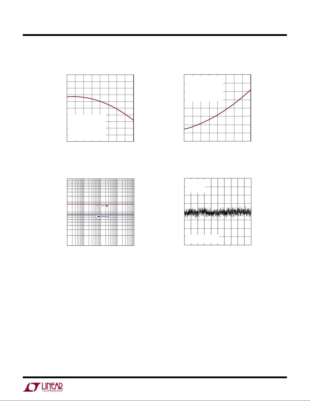
Ripple Rejection (10kHz)
65
63
61
59
57
55
53
VIN = V
OUT(NOMINAL)
RIPPLE = 500mV
51
RIPPLE REJECTION (dB)
f = 10kHz
49
47
45
I
LOAD
C
OUT
C
SET
–50
–25 25
= 0.1A
= 2.2µF
= 0.1µF
0
Noise Spectral Density
1000
+ 2V
P-P
50
TEMPERATURE (°C)
75
100
125
150
100
SPECTRAL DENSITY (pA/√Hz)
REFERENCE CURRENT NOISE
RIPPLE REJECTION (dB)
TJ = 25°C unless otherwise specified.
Ripple Rejection (1MHz)
26
VIN = V
RIPPLE = 200mV
24
f = 1MHz
I
LOAD
22
C
OUT
C
SET
20
18
16
14
12
10
–25
–50
OUT(NOMINAL)
= 0.1A
= 2.2µF CERAMIC
= 0.1µF
+ 2V
P-P
0
50
25
TEMPERATURE (°C)
75
100
125
10Hz to 100kHz
Output Voltage Noise
C
= 0.1µF
SET
= 4.7µF
C
OUT
= 1.5A
I
LOAD
150
3081 G36
100
ERROR AMPLIFIER NOISE
SPECTRAL DENSITY (nV/√Hz)
10
10
FREQUENCY (Hz)
1k100 10k 100k
V
10
1
OUT
50µV/DIV
NOISE INDEPENDENT
OF OUTPUT VOLTAGE
TIME 1ms/DIV
3081 G38
For more information www.linear.com/LT3081
3081fc
9
Page 10
LT3081
3081 BD
pin FuncTions
IN: Input. This pin supplies power to regulate internal
circuitry and supply output load current. For the device
to operate properly and regulate, the voltage on this pin
must be between the dropout voltage and 36V above the
OUT pin (depending on output load current, see Dropout
Voltage Specifications).
OUT: Output. This is the power output of the device. The
LT3081 requires a 5mA minimum load current for proper
output regulation.
TEMP: Temperature Output. This pin delivers a current
proportional to the internal average junction temperature.
Current output is 1µA/°C for temperatures above 5°C. The
TEMP pin output current typically equals 25µA at 25°C.
The output of the TEMP pin is valid for voltages from V
+ 0.4V to V
: Current Limit Program. A resistor between this pin
I
LIM
– 40V. If unused, connect this pin to OUT.
OUT
OUT
and OUT programs output current limit to a level proportional to
OUT
resistor value. Connect this resistor directly to
at the pins of the package. The typical ratio of current
limit to resistor value is 360mA/kΩ with a 450Ω offset.
If programmable current limit is not used, leave this pin
open; the internal current limit of
keeping
the device inside safe operating limits. External
voltage drops between the current limit resistor and V
the LT3081 is still active,
OUT
will affect the current limit. Keep drops below 1mV.
: Output Current Monitor. The I
I
MON
current typically equal to I
LOAD
/5000 or 200µA per amp of
pin sources a
MON
output current. Terminating this pin with a resistor to GND
produces a voltage proportional to I
at I
LOAD
= 1.5A, I
typically sources 300µA. With a
MON
. For example,
LOAD
1k resistor to GND, this produces 300mV. The output
of the I
V
OUT
pin is valid for voltages from V
MON
– 40V. If unused, connect this pin to OUT.
+ 0.4V to
OUT
SET: Set. This pin is the error amplifier’s noninverting
input and also sets the operating bias point of the circuit.
A fixed 50μA current source flows out of this pin. A single
external resistor programs V
. Output voltage range is
OUT
0V to 34.5V.
Exposed Pad/Tab: Output. The exposed pad of the DF and
FE packages and the tab of the R and T7 packages are tied
internally to OUT. As such, tie them directly to OUT (Pins
1-4/Pins 1-5, 8, 9, 16/Pin 4/Pin 4) at the
of
copper area and planes connected to OUT determine
PCB. The amount
the effective thermal resistance of the packages.
NC: No Connection. No connect pins have no connection
to internal circuitry and may be tied to IN, OUT, GND or
floated.
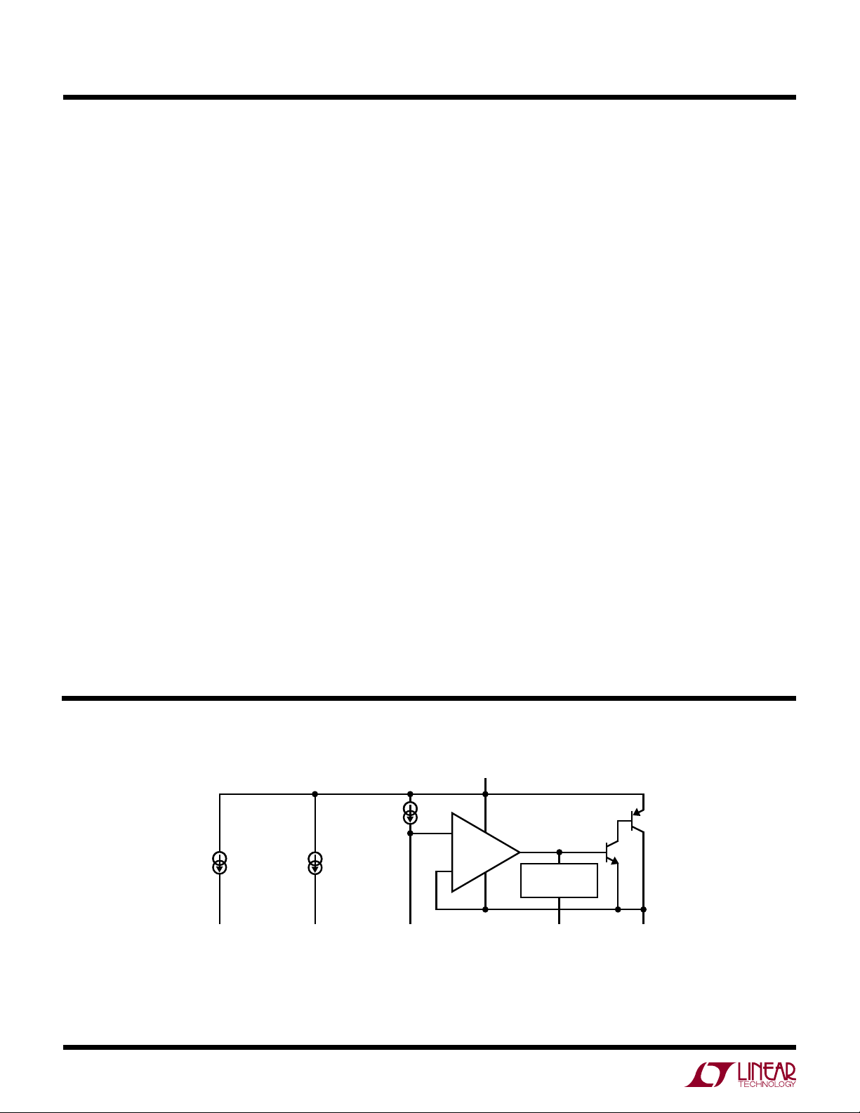
block DiagraM
CURRENT
MONITOR
I
MON
I
MON
10
= I
LOAD
/5000
50µA
+
TEMPERATURE
DEPENDENT
CURRENT SOURCE
1µA/°C
TEMP
For more information www.linear.com/LT3081
SET I
–
IN
PROGRAMMABLE
CURRENT LIMIT
LIM
OUT
3081fc
Page 11
applicaTions inForMaTion
3081 F01
SET
LT3081
Introduction
The LT3081 regulator is easy to use and has all the protection features
expected in high performance regulators.
Included are short-circuit protection, reverse-input protection and
shutdown
the LT3081 is extended, allowing for use in harsh indus
safe operating area protection, as well as thermal
with hysteresis. Safe operating area (SOA) for
trial and automotive environments where sudden spikes
in input voltage lead to high power dissipation.
The LT3081 fits well in applications needing multiple rails.
This new architecture adjusts down to zero with a single
resistor, handling modern low voltage digital ICs as well
as allowing easy parallel operation and thermal manage
ment without heat sinks. Adjusting to zero output allows
shutting off the powered circuitry.
A precision “0” TC 50μA reference current source connects
to the noninverting input of a power operational amplifier.
The power operational amplifier provides a low impedance
buffered output to the voltage on the noninverting input.
A single resistor from the noninverting input to ground
sets the output voltage. If this resistor is set to 0Ω, zero
output voltage results. Therefore, any output voltage can
be obtained between zero and the maximum defined by
the input power supply is
benefit of using a true internal current source as the
The
obtainable.
reference, as opposed to a bootstrapped reference in older
regulators, is not so obvious in this architecture. A true
reference current source allows the regulator to have gain
and frequency response independent of the impedance on
the positive input. On older adjustable regulators, such as
the LT1086 loop gain changes with output voltage and
bandwidth changes if the adjustment pin is bypassed to
ground. For the LT3081, the loop gain is unchanged with
output voltage changes or bypassing. Output regulation
is not a fixed percentage of output voltage, but is a fixed
fraction of millivolts. Use of a true current source allows
all of the gain in the buffer amplifier to provide regulation,
and none of that gain is needed to amplify up the reference
to a higher output voltage.
The LT3081 has many additional features that facilitate
monitoring and control. Current limit is externally pro
grammable via a single resistor between the I
pin and
LIM
-
OUT. Shorting this resistor out disables all output current
to the load, only bias currents remain.
The I
load current. For every 1A of load current, the I
pin produces a current output proportional to
MON
MON
pin
sources 200µA of current. This can be sensed using an
external resistor to monitor load requirements and detect
potential faults. The I
pin can operate at voltages above
MON
OUT, so it operates even during a short-circuit condition.
One additional monitoring function is the TEMP pin, a cur
rent source that is proportional to average die temperature.
For die temperatures above 0°C, the TEMP pin sources a
current equal to 1µA/°C. This pin operates normally during
output short-circuit conditions.
Programming Linear Regulator Output Voltage
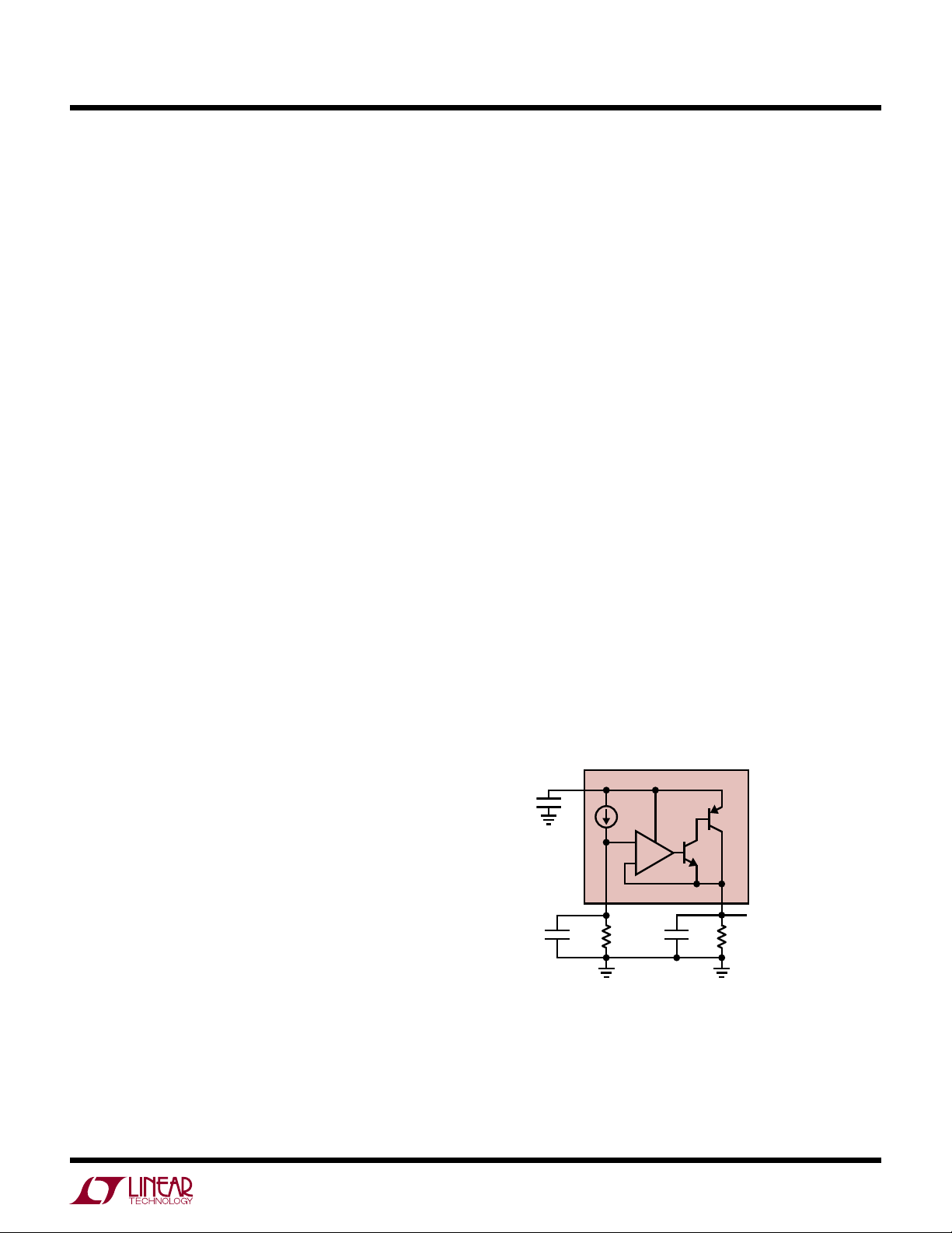
The LT3081 generates a 50μA reference current that flows
out of the SET pin. Connecting a resistor from SET to
ground generates a voltage that becomes the reference
point for the error amplifier (see Figure 1). The reference
voltage equals 50µA multiplied by the value of the SET
pin resistor. Any voltage can be generated and there is
no minimum output voltage for the regulator.
IN
C
IN
C
SET
Figure 1. Basic Adjustable Regulator
LT3081
50µA
+
–
SET OUT
R
SET
C
R
OUT
LOAD
V
OUT
= 50µA • R
For more information www.linear.com/LT3081
3081fc
11
Page 12
LT3081
SET PIN
OUT
OUT
applicaTions inForMaTion
Table 1 lists many common output voltages and the closest standard 1%
resistor values used to generate that
output voltage.
Regulation of the output voltage requires a minimum load
current of 5mA. For true zero voltage output operation,
return this 5mA load current to a negative output voltage.
Table 1. 1% Resistors for Common Output Voltages
V
(V) R
OUT
1 20
1.2 24.3
1.5 30.1
1.8 35.7
2.5 49.9
3.3 66.5
5 100
SET
(kΩ)
With the 50µA current source used to generate the reference
voltage, leakage paths to or from the SET pin can create
errors in the reference and output voltages. High quality
insulation should be used (e.g., Teflon, Kel-F); cleaning of
all insulating surfaces to remove fluxes and other residues
is required. Surface coating may be necessary to provide
a moisture barrier in high humidity environments.
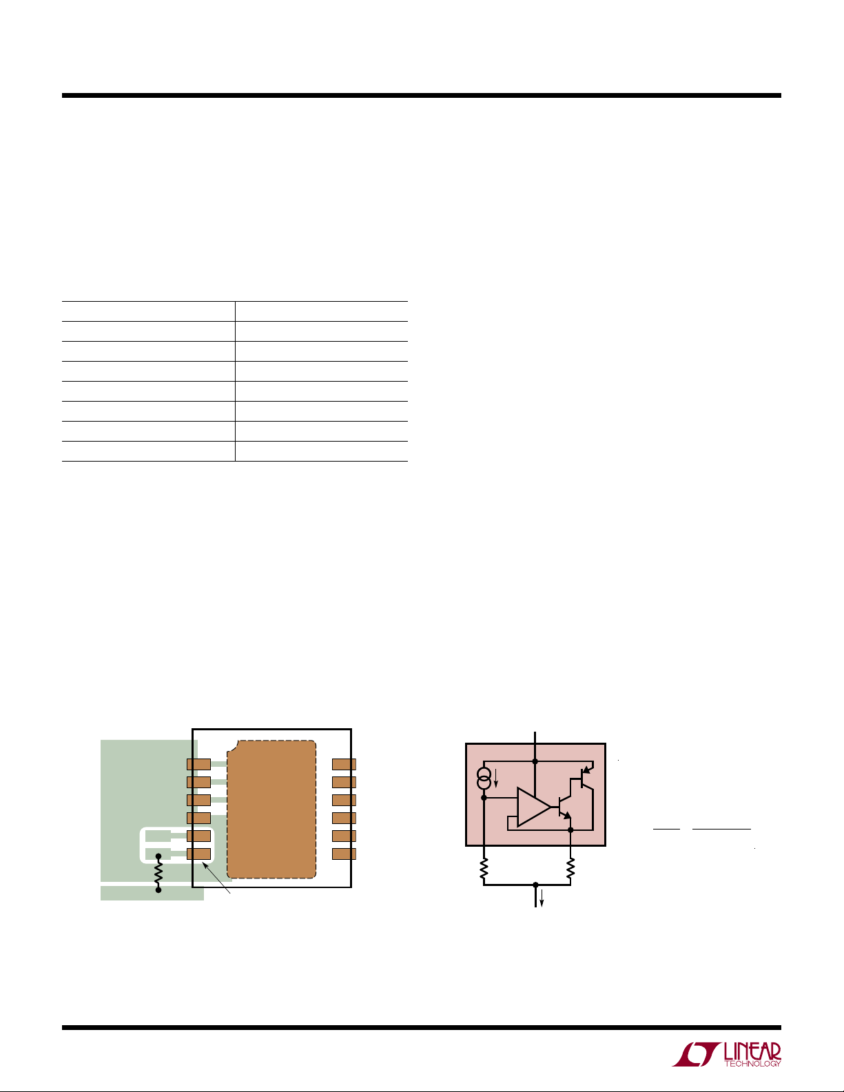
Minimize board leakage by encircling the SET pin and
circuitry with a guard ring operated at a potential close
to itself. Tie the guard ring to the OUT pin. Guarding both
sides of the circuit board is required. Bulk leakage reduction
depends on
out
of the SET pin and its associated circuitry creates a
the guard ring width. 50nA of leakage into or
0.1% reference voltage error. Leakages of this magnitude,
coupled with other sources of leakage, can cause signifi
cant offset voltage and reference drift, especially over the
possible
operating temperature range. Figure 2 depicts an
example guard ring layout.
If guard ring techniques are used, this bootstraps any
stray capacitance at the SET pin. Since the
a
high impedance node, unwanted signals may couple
SET pin is
into the SET pin and cause erratic behavior. This will
be most noticeable when operating with minimum
output capacitors at full load current. The easiest way
to remedy this is to bypass the SET pin with a small
amount of capacitance from SET to ground, 10pF to
20pF is sufficient.
Configuring the LT3081 as a Current Source
Setting the LT3081 to operate as a 2-terminal current
source is a simple matter. The 50µA reference current from
the SET pin is used with one resistor to generate a small
voltage, usually in the range of 100mV to 1V (200mV is a
level that rejects offset voltage, line regulation, and other
errors without being excessively large). This voltage is
then applied across a second resistor that connect from
OUT to the first resistor. Figure 3 shows connections and
formulas to calculate a basic current source configuration.
-
50µA
IN
I
≥ 5mA
OUT
V
I
SET
OUT
= 50µA •R
V
SET
=
R
SET
50µA • R
=
SET
R
3081fc
+
–
3081 F03
R
OUT
I
OUT
OUT
GND
Figure 2. Guard Ring Layout Example of DF Package Figure 3. Using the LT3081 as a Current Source
12
3081 F02
For more information www.linear.com/LT3081
LT3081
SET OUT
+
V
R
SET
SET
–
Page 13

applicaTions inForMaTion
LT3081
Again, the lower current levels used in the LT3081 necessitate attention
to board leakages as error sources (see the
Programming Linear Regulator Output Voltage section).
In a current source configuration, programmable cur-
rent limit and current monitoring functions are often
unused. When not used, tie I
to OUT and leave I
MON
LIM
open. The TEMP pin is still available for use, if unused tie
TEMP to OUT.
Selecting R
In Figure 3, both resistors R
SET
and R
in Current Source Applications
OUT
SET
and R
program the
OUT
value of the output current. The question now arises: the
ratio of these resistors is known, but what value should
each resistor be?
The first resistor to select is R
. The value selected should
SET
generate enough voltage to minimize the error caused by
the offset between the SET and OUT pins. A reasonable
(R
starting level is ~200mV of voltage across R
SET
SET
equal
to 4.02k). Resultant errors due to offset voltage are a few
percent. The lower the voltage across R
becomes, the
SET
higher the error term due to the offset.
Programming Current Limit Externally
A resistor placed between I
and OUT on the LT3081
LIM
externally sets current limit to a level lower than the internal
current limit. Connect this resistor directly at the OUT pins
for best accuracy. The value of this resistor calculates as:
R
The resistor for a 1.3A current limit is: R
ILIM
= I
/360mA/kΩ + 450Ω
LIMIT
= 1.3A/360mA/
ILIM
kΩ + 450Ω = 4.06k. Tolerance over temperature is ±15%,
so current limit is normally set 20% above maximum load
current. The 450Ω offset resistance built in to the pro
grammable current
limit allows for lowering the maximum
output current to only bias currents (see curve of Minimum
Load Current in Typical Performance Characteristics) us
ing external switches.
The LT3081’s internal current limit overrides the programmed current
limit if the input-to-output voltage differential in the power transistor is excessive. The internal
current
limit is ≈2A with a foldback characteristic dependent
on input-to-output differential voltage, not output voltage
per se (see Typical Performance Characteristics).
-
-
From this point, selecting R
forward calculation from
R
is easy, as it is a straight-
OUT
. Take note, however, resistor
SET
errors must be accounted for as well. While larger voltage
drops across R
minimize the error due to offset, they
SET
also increase the required operating headroom.
Obtaining the best temperature coefficient does not require
the use of expensive resistors with low ppm temperature
coefficients. Instead, since the output current of the LT3081
is determined by the ratio of R
SET
to R
, those resis-
OUT
tors should have matching temperature characteristics.
expensive resistors made from the same material
Less
provide matching temperature coefficients. See resistor
manufacturers’ data sheets for more details.
Higher output currents necessitate the use of higher watt
age resistors
for R
the resistors used for R
. There may be a difference between
OUT
OUT
and R
. A better method to
SET
-
maintain consistency in resistors is to use multiple resis-
parallel to create R
tors in
and type of resistor as R
, allowing the same wattage
OUT
.
SET
Stability and Input Capacitance
The LT3081 does not require an input capacitor to main
tain stability. Input capacitors are recommended in linear
regulator configurations to provide a low impedance input
source to the LT3081. If using an input capacitor, low
ESR, ceramic input bypass capacitors are acceptable for
applications without long input leads. However, applica
tions connecting
a power supply to an LT3081 circuit’s
-
IN and GND pins with long input wires combined with
low ESR, ceramic input capacitors
spikes,
reliability concerns and application-specific board
are prone to voltage
oscillations. The input wire inductance found in many
battery-powered applications, combined with the low ESR
ceramic input capacitor, forms a high Q LC resonant tank
circuit. In some instances this resonant frequency beats
against the output current dependent LDO bandwidth and
interferes with proper operation. Simple circuit modifica
tions/solutions are
then required. This behavior is not
-
indicative of LT3081 instability, but is a common ceramic
input bypass capacitor application issue.
For more information www.linear.com/LT3081
3081fc
13
Page 14

LT3081
applicaTions inForMaTion
The self-inductance, or isolated inductance, of a wire is
directly proportional to its length. Wire diameter is not a
major factor on its self-inductance. For example, the selfinductance of a 2-AWG isolated wire (diameter = 0.26") is
about half the self-inductance of a 30-AWG wire (diameter
= 0.01"). One foot of 30-AWG wire has about 465nH of
self inductance.
One of two ways reduces a wire’s self-inductance. One
method divides the current flowing towards the LT3081
between two parallel conductors. In this case, the farther
apart the wires are from each other, the more the selfinductance is reduced; up to a 50% reduction when placed
a few inches apart. Splitting the wires basically connects
two equal inductors in parallel, but placing them in close
proximity gives the wires mutual inductance adding to
the self-inductance. The second and most effective way
to reduce overall inductance is to place both forward and
return current conductors (the input and GND wires) in
very close proximity. Tw o 30-AWG wires separated by
only 0.02", used as forward and return current conduc
tors, reduce
one-fifth that of a single isolated wire.
If wiring modifications are not permissible for the applications, including
and the input of the LT3081 also stabilizes the application.
As little as 0.1Ω to 0.5Ω, often less, is effective in damp
ing the LC resonance. If the added impedance between
the power supply and the input is unacceptable, adding
ESR to the input capacitor also provides the necessary
damping of the LC resonance. However, the required ESR
is generally higher than the series impedance required.
Stability and Frequency Compensation for Linear
Regulator Configurations
The LT3081 does not require an output capacitor for
stability. LT C recommends an output capacitor of 10μF
with an ESR of 0.5Ω or less to provide good transient
performance in linear regulator configurations. Larger
values of output capacitance decrease peak deviations and
provide improved transient response for larger load current
changes. Bypass capacitors, used to decouple individual
components powered by the LT3081, increase the effec
tive output capacitor value. For improvement in transient
the overall self-inductance to approximately
series
resistance between the power supply
-
-
-
performance, place a capacitor across the voltage setting
resistor. Capacitors up to 1μF can be used. This bypass
capacitor reduces system noise as well, but start-up time
is proportional to the time constant of the voltage
resistor (
Stability and Frequency Compensation for Current
Source Configurations
The LT3081 does not require input or output capacitors
for stability in many current-source applications. Clean,
tight PCB layouts provide a low reactance, well controlled
operating environment for the LT3081 without requiring
capacitors to frequency compensate the circuit. Figure 3
highlights the simplicity of using the LT3081 as a current
source.
Some current source applications use a capacitor con
nected in
current
soft-start function for the current source. See Quieting the
Noise section for further details. When operating without
output capacitors, the high impedance nature of the SET
pin as the input of the error amplifier allows signal from
the output to couple in, showing as high frequency ring
ing during transients. Bypassing the SET resistor with a
capacitor
Depending on the pole introduced by a capacitor or other
complex impedances presented to the LT3081, external
compensation may be required for stability. Techniques
are discussed to achieve this in the following paragraphs.
Linear Technology strongly recommends testing stability
in
situ with final components before beginning production.
Although the LT3081’s design strives to be stable without
capacitors over a wide variety of operating conditions, it is
not possible to test for all possible combinations of input
and output impedances that the LT3081 will encounter.
These impedances may include resistive, capacitive, and
inductive components and may be complex distributed
networks. In addition, the current source’s value will dif
fer between applications and its connection may be GND
referenced, power supply referenced, or floating in a signal
line path. Linear Technology strongly recommends that
stability be tested in situ for any LT3081 application.
R
in Figure 1) and SET pin bypass capacitor.
SET
parallel with the SET pin resistor to lower the
source’s noise. This capacitor also provides a
in the range of 20pF to 30pF dampens the ringing.
setting
-
-
-
14
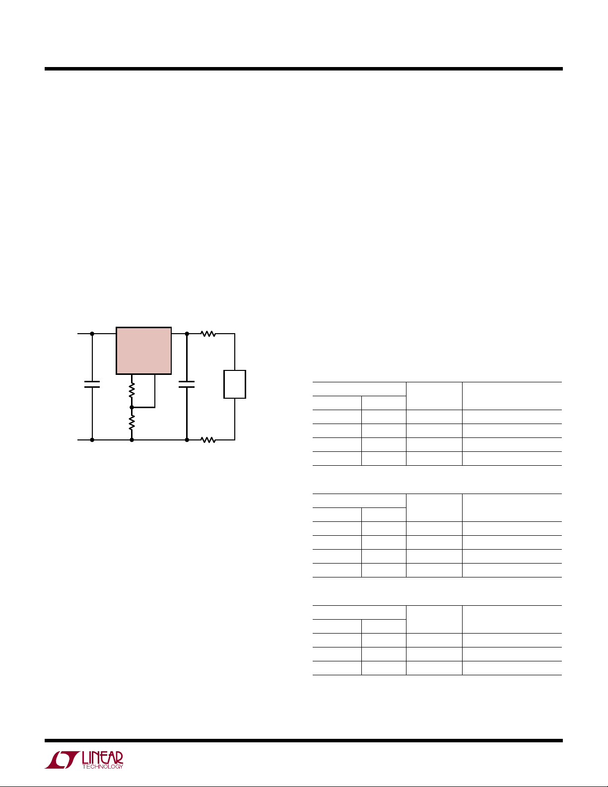
3081fc
For more information www.linear.com/LT3081
Page 15
applicaTions inForMaTion
LT3081
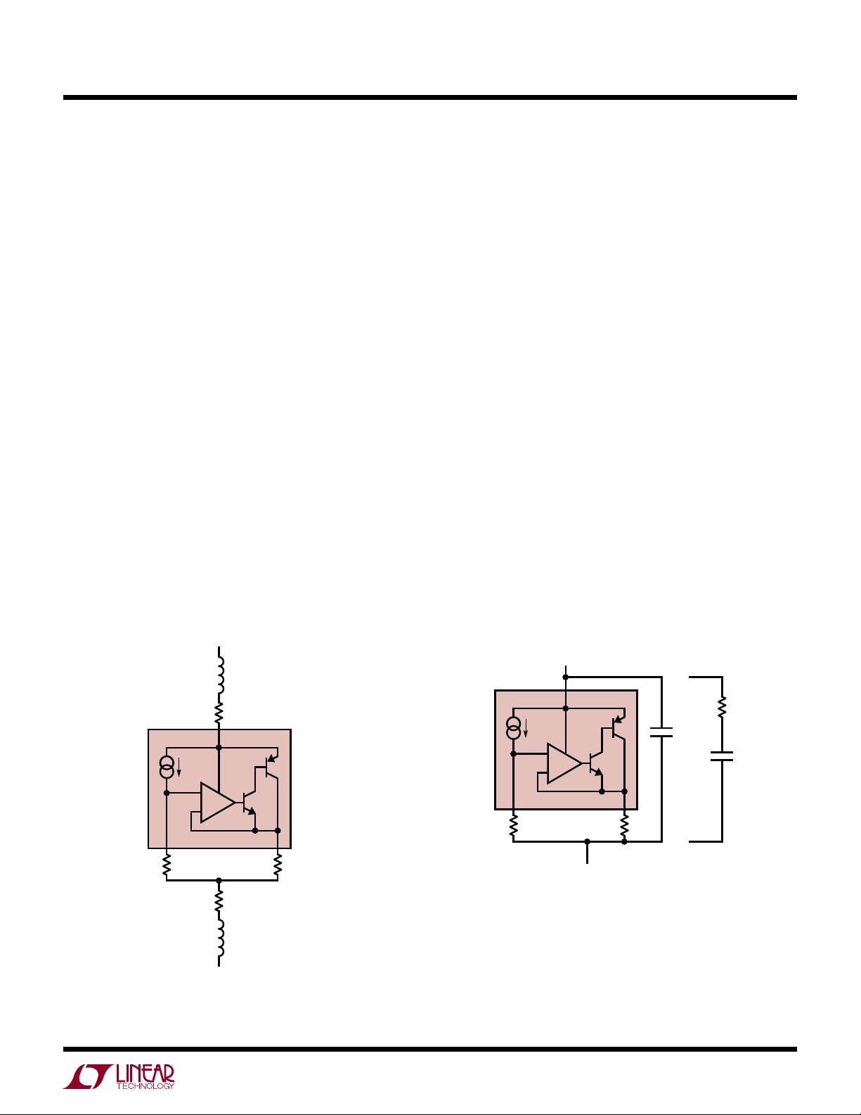
In LT3081 applications with long wires or PCB traces, the
inductive reactance may cause instability. In some cases,
adding series resistance to the input and output lines (as
shown in Figure 4) may sufficiently dampen these possible
high-Q lines and provide stability. The user must evaluate
the required resistor values against the design’s headroom
constraints. In general, operation at low output current
levels (<20mA) automatically requires higher values of
programming resistors and may provide the necessary
damping without additional series impedance.
If the line impedances in series with the LT3081 are
complex enough such that series damping resistors are
not sufficient, a frequency compensation network may be
necessary. Several options may be considered.
Figure 5 depicts the simplest frequency compensation
networks as a single capacitor across the two terminals
of the current source. Some applications may use the
capacitance to stand off DC voltage but allow the transfer
of data down a signal line.
For some applications, pure capacitance may be unac
ceptable or
present
a design constraint. One circuit
-
example typifying this is an “intrinsically-safe” circuit in
which an overload or fault condition potentially allows the
capacitor’s stored
plications where
energy to create a spark or arc. For ap-
a single capacitor is unacceptable, Figure
5 alternately shows a series RC network connected across
the two terminals of the current source. This network has
the added benefit of limiting the discharge current of the
capacitor under a fault condition, preventing sparks or
arcs. In many instances, a series RC network is the best
solution for stabilizing the application circuit. Typical resis
tor values will range from 100Ω to 5k. Once again, Linear
T
echnology strongly recommends testing stability in situ
for any LT3081 application across all operating conditions,
especially ones that present complex impedance networks
at the input and output of the current source.
If an application refers the bottom of the LT3081 current
source to GND, it may be necessary to bypass the top
of the current source with a capacitor to GND. In some
cases, this capacitor may already exist and no additional
capacitance is required. For example, if the LT3081 was
used as a variable current source on the output of a power
supply, the output bypass capacitance would suffice to
provide LT3081 stability. Other applications may require
the addition of a bypass capacitor. A series RC network
may also
plication requirements.
be used as necessary, and depends on the ap-
-
LONG LINE
REACTANCE/INDUCTANCE
R
SERIES
50µA
IN
+
–
3081 F04
R
SERIES
LONG LINE
REACTANCE/INDUCTANCE
R
OUT
LT3081
SET OUT
R
SET
Figure 4. Adding Series Resistance Decouples
and Dampens Long Line Reactances
50µA
IN
C
COMP
+
–
R
OUT
3081 F05
OR
R
COMP
C
COMP
LT3081
SET OUT
R
SET
Figure 5. Compensation from Input to Output
of Current Source Provides Stability
3081fc
For more information www.linear.com/LT3081
15
Page 16
LT3081
3081 F08
applicaTions inForMaTion
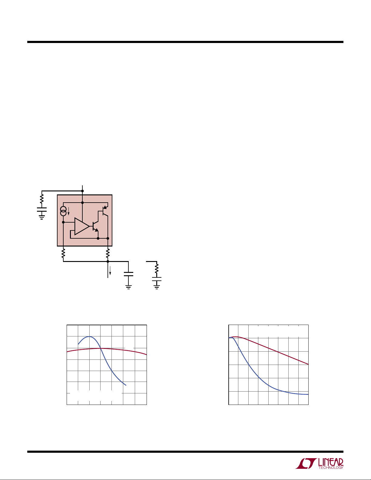
In some extreme cases, capacitors or series RC networks
may be required on both the LT3081’s input and output to
stabilize the circuit. Figure 6 depicts a general application
using input and output capacitor networks rather than
an input-to-output capacitor. As the input of the current
source tends to be high impedance, placing a capacitor
on the input does not have the same effect as placing a
capacitor on the lower impedance output. Capacitors in the
range of 0.1µF to 1µF usually provide sufficient bypassing
on the input, and the value of input capacitance may be
increased without limit. Pay careful attention to using low
ESR input capacitors with long input lines (see the Stabil
-
ity and Input Capacitance section for more information).
V
IN
R
LT3081
IN
C
IN
SET OUT
Figure 6. Input and/or Output Capacitors May
Be Used for Compensation
IN
50µA
+
–
R
SET
R
OUT
R
I
OUT
C
OR
OUT
OUT
C
3081 F06
OUT
Using Ceramic Capacitors
Give extra consideration to the use of ceramic capacitors.
Ceramic capacitors are manufactured with a variety of di
electrics, each with different behavior across temperature
and applied voltage. The most common dielectrics used
are specified with EIA temperature characteristic codes of
Z5U, Y5V, X5R and X7R. The Z5U and Y5V dielectrics are
good for providing high capacitances in a small package,
but they tend
coefficients
to have strong voltage and temperature
as shown in Figures 7 and 8. When used with
a 5V regulator, a 16V 10μF Y5V capacitor can exhibit an
effective value as low as 1μF to 2μF for the DC bias voltage
applied and over the operating temperature range. The X5R
and X7R dielectrics result in more stable characteristics
and are more suitable for use as the output capacitor.
The X7R type has better stability across temperature,
while the X5R is less expensive and is available in higher
values. Care still must be exercised when using X5R and
X7R capacitors. The X5R and X7R codes only specify
operating temperature range and maximum capacitance
change over temperature. Capacitance change due to DC
bias with X5R and X7R capacitors is better than Y5V and
Z5U capacitors, but can still be significant enough to drop
capacitor values below appropriate levels. Capacitor DC
bias characteristics tend to improve as component case
size increases, but expected capacitance at operating
voltage should be verified.
16
40
20
0
–20
–40
–60
CHANGE IN VALUE (%)
–80
BOTH CAPACITORS ARE 16V,
1210 CASE SIZE, 10µF
–100
–50
–25 0
TEMPERATURE (°C)
Y5V
50 100 125
25 75
X5R
3081 F07
For more information www.linear.com/LT3081
Figure 8. Ceramic Capacitor DC Bias CharacteristicsFigure 7. Ceramic Capacitor Temperature Characteristics
20
0
–20
–40
–60
CHANGE IN VALUE (%)
–80
–100
0
BOTH CAPACITORS ARE 16V,
1210 CASE SIZE, 10µF
2 6
4
DC BIAS VOLTAGE (V)
X5R
Y5V
14
8
12
10
16
3081fc
Page 17
applicaTions inForMaTion
LT3081
Voltage and temperature coefficients are not the only
sources of problems. Some ceramic capacitors have a
piezoelectric response. A piezoelectric device generates
voltage across its terminals due to mechanical stress. In a
ceramic capacitor, the stress can be induced by vibrations
in the system or thermal transients.
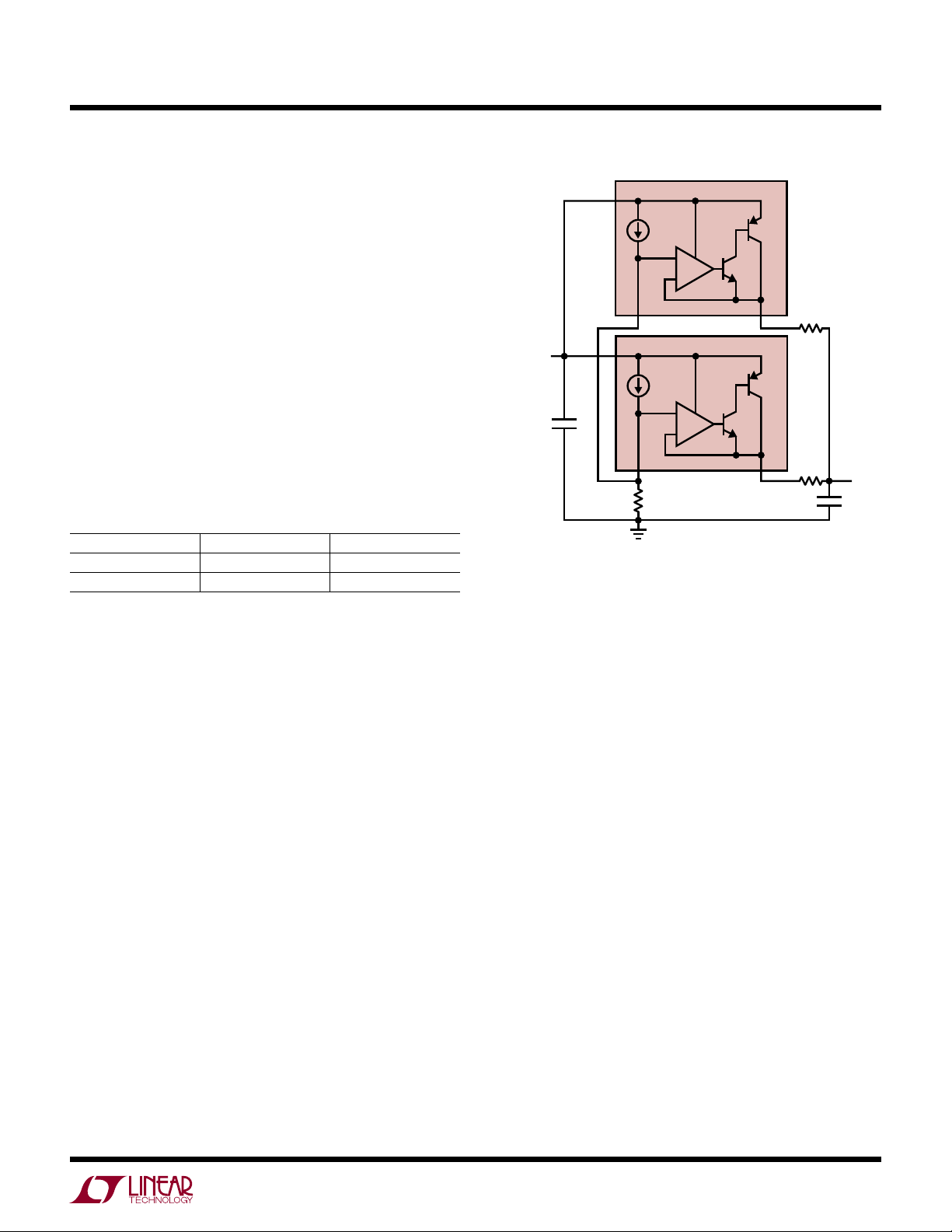
Paralleling Devices
Higher output current is obtained by paralleling multiple
LT3081s together. Tie the individual SET pins together and
tie the individual IN pins together. Connect the outputs in
common using small pieces of PC trace as ballast resistors
to promote equal current sharing. PC trace resistance in
milliohms/inch is shown in Table 2. Ballasting requires
only a tiny area on the PCB.
Table 2. PC Board Trace Resistance
WEIGHT (oz) 10mil WIDTH 20mil WIDTH
1 54.3 27.1
2 27.1 13.6
Trace resistance is measured in mΩ/in.
The worst-case room temperature offset, only ±1.5mV
between the SET pin and the OUT pin, allows the use of
very small ballast resistors.
As shown in Figure 9, each LT3081 has a small 10mΩ
ballast resistor, which at full output current gives better
than 80% equalized sharing of the current. The external
resistance of 10mΩ (5mΩ for the two devices in parallel)
only adds about 15mV of output regulation drop at an
output of 3A. Even with an output voltage as low as 1V,
this only adds 1.5% to the regulation. Of course, paralleling
more than two LT3081s yields even higher output current.
Spreading the devices on the PC board also spreads the
heat. Series input resistors can further spread the heat if
the input-to-output difference is high.
If the increase in load regulation from the ballast resistors is unacceptable, the I
compensate for these drops (see Using I
output can be used to
MON
MON
Cancels
Ballast Resistor Drop in the Typical Applications section).
Regulator paralleling without the use of ballast resistors is
I
accomplished by comparing the
tors (see Load
Current Sharing Without Ballasting in the
outputs of regula-
MON
Typical Applications section).
SET
SET
33k
50µA
50µA
LT3081
+
–
LT3081
+
–
OUT
OUT
10mΩ
10mΩ
10µF
3081 F09
V
OUT
3.3V
3A
V
4.8V TO 40V
IN
IN
IN
1µF
Figure 9. Parallel Devices
Quieting the Noise
The LT3081 offers numerous noise performance advantages. Ever
general,
y linear regulator has its sources of noise. In
a linear regulator’s critical noise source is the
reference. In addition, consider the error amplifier’s noise
contribution along with the resistor divider’s noise gain.
Many traditional low noise regulators bond out the voltage
reference to an external pin (usually through a large value
resistor) to allow for bypassing and noise reduction. The
LT3081 does not use a traditional voltage reference like
other linear regulators. Instead, it uses a 50µA reference
current. The 50µA current source generates noise current
levels of 18pA/√Hz (5.7nA
over a 10Hz to 100kHz
RMS
bandwidth). The equivalent voltage noise equals the RMS
noise current multiplied by the resistor value.
The SET pin resistor generates spot noise equal to √4kTR
–23
(k = Boltzmann’s constant, 1.38 • 10
lute temperature)
which is RMS summed with the voltage
J/°K, and T is abso-
noise. If the application requires lower noise performance,
bypass the voltage setting resistor with a capacitor to GND.
Note that this noise-reduction capacitor increases
start-up
time as a factor of the RC time constant.
For more information www.linear.com/LT3081
3081fc
17
Page 18
LT3081
applicaTions inForMaTion
The LT3081 uses a unity-gain follower from the SET pin
to the OUT pin. Therefore, multiple possibilities exist
(besides a SET pin resistor) to set output voltage. For
example, using a high accuracy voltage reference from
SET to GND removes the errors in output voltage due to
reference current tolerance and resistor tolerance. Active
driving of the SET pin is acceptable.
The typical noise scenario for a linear regulator is that the
output voltage setting resistor divider gains up the reference
noise, especially if V
is much greater than V
OUT
REF
. The
LT3081’s noise advantage is that the unity-gain follower
presents no noise gain whatsoever from the SET pin to the
output. Thus, noise figures do not increase accordingly.
Error amplifier noise is typical 85nV/√Hz(27µV
RMS
over
a 10Hz to 100kHz bandwidth). The error amplifier’s noise
is RMS summed with the other noise terms to give a final
noise figure for the regulator.
Paralleling of regulators adds the benefit that output noise
is reduced. For n regulators in parallel, the output noise
drops by a factor of √n.
Curves in the Typical Performance Characteristics sec
tion show
characteristics
noise spectral density and peak-to-peak noise
for both the reference current and error
-
amplifier over a 10Hz to 100kHz bandwidth.
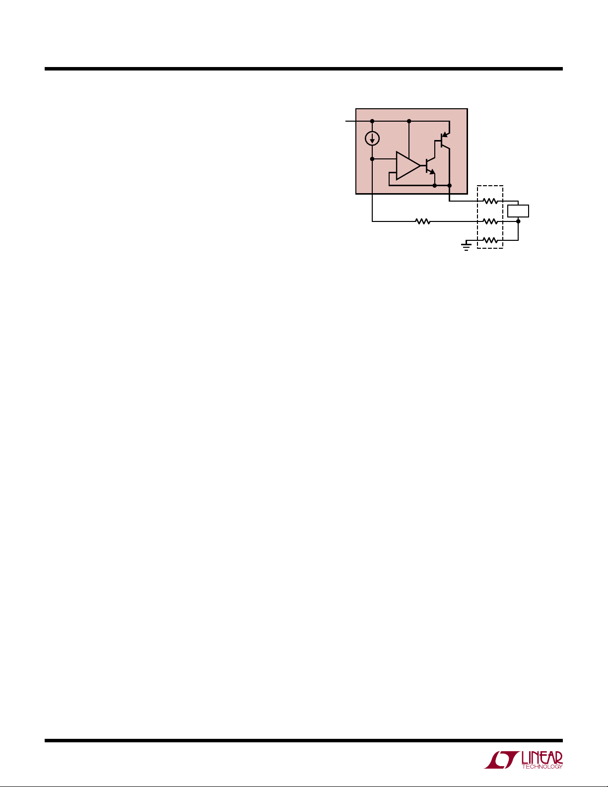
Load Voltage Regulation
The LT3081 is a floating device. No ground pin exists on
the packages. Thus, the IC delivers all quiescent current
and drive current to the load. Therefore, it is not possible
to provide true remote load sensing. The connection re
sistance between
the regulator and the load determines
-
load regulation performance. The data sheet’s load
regulation specification is Kelvin sensed at the package’s
pins. Negative-side sensing is a true Kelvin connection by
returning the bottom of the voltage setting resistor to the
negative side of the load (see Figure 10).
Connected as shown, system load regulation is the sum
of the LT3081’s load regulation and the parasitic line
resistance multiplied by the output current. To minimize
load regulation, keep the positive connection between the
regulator and load as short as possible. If possible, use
large diameter wire or wide PC board traces.
SET
50µA
LT3081
+
–
PARASITIC
RESISTANCE
OUT
R
SET
R
P
LOAD
R
P
R
P
3081 F10
IN
Figure 10. Connections for Best Load Regulation
TEMP Pin Operation (Die Temperature Monitor)
The TEMP pin of the LT3081 outputs a current proportional
to average die temperature. At 25°C, the current from the
TEMP pin is 25µA, with a slope
of 1µA/°C. The current out
of the TEMP pin is valid for junction temperatures above
0°C (absent initial offset considerations). Below 0°C, the
TEMP pin will not sink current to indicate die temperature.
The TEMP pin output current is valid for voltages up to
40V below and 0.4V above the OUT pin allowing operation
even during short-circuit conditions.
Connecting a resistor from TEMP to ground converts the
TEMP pin current into a voltage to allow for monitoring
by an ADC. With a 1k resistor, 0mV to 150mV indicates
0°C to 150°C.
It should be noted that the TEMP pin current represents an
average temperature and should not be used to guarantee
that maximum junction temperature is not exceeded.
Instantaneous power along with thermal gradients and
time constants may cause portions of the die to exceed
maximum ratings and thermal shutdown thresholds. Be
sure to calculate die temperature rise for steady state (>1
minute) as well as impulse conditions.
Pin Operation (Current Monitor)
I
MON
The LT3081’s I
the load current supplied at a ratio of 1:5000. The I
pin outputs a current proportional to
MON
MON
pin current is valid for voltages up to 40V below and 0.4V
the OUT pin, allowing operation even during short-
above
cir
cuit conditions.
18
3081fc
For more information www.linear.com/LT3081
Page 19
applicaTions inForMaTion
LT3081
Connecting a resistor from I
pin current into a voltage to allow for monitoring by
I
MON
to ground converts the
MON
an ADC. With a 1k resistor, 0mV to 300mV indicates 0A
to 1.5A of load current.
Compensating for Cable Drops with I
The I
pin can compensate for resistive drops in wires
MON
MON
or cables between the LT3081 and the load. Breaking the
SET resistor into two pieces adjusts the output voltage as a
function of load current. The ratio of the output wire/cable
impedance to the bottom resistor should be 1:5000. The
sum total of the two SET resistor values determines the
initial output voltage. Figure 11 shows a typical application
and formulas for calculating resistor values.
R
CABLE2
IN
SET
C
IN
1µF
R
= 5000 • R
COMP
V
OUT(LOAD)
CABLE(TOTAL)
= 50µA (R
Figure 11. Using I
OUT
LT3081
I
MON
R
SET
29.8k
R
COMP
200Ω
+ R
SET
COMP
to Compensate for Cable Drops
MON
0.02Ω
C
OUT
R
CABLE
0.02Ω
LOAD
3081 F11
10µF
)
Thermal Considerations
The LT3081’s internal power and thermal limiting circuitry
protects itself under overload conditions. For continuous
normal load conditions, do not exceed the 125°C (E- and
I-grades) or 150°C (H- and MP-grades) maximum junc
.
tion temperature
Carefully consider all sources of thermal
-
resistance from junction-to-ambient. This includes (but is
not limited to) junction-to
face,
heat sink resistance or circuit board-to-ambient as
application dictates. Consider all additional, adjacent
the
-case, case-to-heat sink inter-
heat generating sources in proximity on the PCB.
Surface mount packages provide the necessary heat
sinking by using the heat spreading capabilities of the
PC board, copper traces and planes. Surface mount heat
sinks, plated through-holes and solder-filled vias can also
spread the heat generated by power devices.
Junction-to-case thermal resistance is specified from the
IC junction to the bottom of the case directly, or the bot
tom of the pin most directly in the heat path. This is the
lowest thermal resistance path for heat flow. Only proper
device mounting ensures the best possible thermal flow
from this area of
the packages to the heat sinking material.
Note that the exposed pad of the DFN and TSSOP packages and
are electrically connected to the output (V
the tab of the DD-Pak and TO-220 packages
).
OUT
Tables 3 through 5 list thermal resistance as a function
of copper areas on a fixed board size. All measurements
were taken in still air on a 4-layer FR-4 board with 1oz
solid internal planes and 2oz external trace planes with a
total finished board thickness of 1.6mm.
Table 3. DF Package, 12-Lead DFN
COPPER AREA
BOARD AREA
2
2500mm
1000mm
225mm
100mm
*Device is mounted on topside
2500mm22500mm
2
2500mm22500mm
2
2500mm22500mm
2
2500mm22500mm
Table 4. FE Package, 16-Lead TSSOP
COPPER AREA
BOARD AREA
2
2500mm
1000mm
225mm
100mm
*Device is mounted on topside
2500mm22500mm
2
2500mm22500mm
2
2500mm22500mm
2
2500mm22500mm
Table 5. R Package, 7-Lead DD-Pak
COPPER AREA
BOARD AREA
2500mm2 2500mm2 2500mm2 13°C/W
1000mm2 2500mm2 2500mm2 14°C/W
225mm2 2500mm2 2500mm2 16°C/W
*Device is mounted on topside
THERMAL RESISTANCE
(JUNCTION-TO-AMBIENT)TOPSIDE* BACKSIDE
2
2
2
2
THERMAL RESISTANCE
(JUNCTION-TO-AMBIENT)TOPSIDE* BACKSIDE
2
2
2
2
THERMAL RESISTANCE
(JUNCTION-TO-AMBIENT)TOPSIDE* BACKSIDE
18°C/W
22°C/W
29°C/W
35°C/W
16°C/W
20°C/W
26°C/W
32°C/W
For more information www.linear.com/LT3081
3081fc
19
Page 20
LT3081
7V – 3.3V – 1.5V
1.5A
applicaTions inForMaTion
T7 Package, 7-Lead TO-220
Thermal Resistance (Junction-to-Case) = 3°C/W
For further information on thermal resistance and using
thermal information, refer to JEDEC standard JESD51,
notably JESD51-12.
PCB layers, copper weight, board layout and thermal vias
affect the resultant thermal resistance. Tables 3 through 5
provide thermal resistance numbers for best-case 4-layer
boards with 1oz internal and 2oz external copper. Modern,
multilayer PCBs may not be able to achieve quite the same
level performance as found in these tables. Demo circuit
1870A’s board layout using multiple inner V
OUT
planes
and multiple thermal vias achieves 16°C/W performance
for the FE package.
Calculating Junction Temperature
Example: Given an output voltage of 0.9V, an IN voltage
of 2.5V ±5%, output current range from 10mA to 1A
and a maximum ambient temperature of 50°C, what is
the maximum junction temperature for the DD-Pak on a
2
2500mm2 board with topside copper of 1000mm
?
The power in the circuit equals:
P
TOTAL
= (VIN – V
OUT
)(I
OUT
)
The current delivered to the SET pin is negligible and can
be ignored.
V
IN(MAX_CONTINUOUS)
V
= 0.9V, I
OUT
OUT
= 2.625V (2.5V + 5%)
= 1A, TA = 50°C
Power dissipation under these conditions equals:
P
TOTAL
= (VIN – V
OUT
)(I
OUT
)
Reducing
In
some applications it may be necessary to reduce the
Power Dissipation
power dissipation in the LT3081 package without sacrificing
output current capability. Tw o techniques are available. The
first technique, illustrated in Figure 12, employs a resis
series with the regulator’s input. The voltage drop
tor in
across
decreases the LT3081’s IN-to-OUT differential
R
S
-
voltage and correspondingly decreases the LT3081’s
power dissipation.
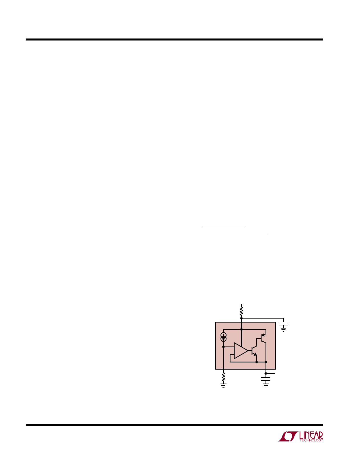
As an example, assume: V
= 7V, V
IN
= 3.3V and I
OUT
OUT(MAX)
= 1.5A. Use the formulas from the Calculating Junction
Temperature section previously discussed.
Without series resistor R
, power dissipation in the
S
LT3081 equals:
P
If the voltage differential (V
chosen as 1.5V, then R
= (7V – 3.3V) • 1.5A = 5.55W
TOTAL
equals:
S
RS=
) across the LT3081 is
DIFF
= 1.5Ω
Power dissipation in the LT3081 now equals:
P
= 1.5V • 1.5A = 2.25W
TOTAL
The LT3081’s power dissipation is now only 40% compared
to no series resistor. R
dissipates 3.3W of power. Choose
S
appropriate wattage resistors or use multiple resistors in
parallel to handle and dissipate the power properly.
V
IN
R
S
′
V
LT3081
IN
IN
C1
P
= (2.625V – 0.9V)(1A) = 1.73W
TOTAL
Junction Temperature equals:
= TA + P
T
J
= 50°C + 1.73W • 14°C/W = 74.2°C
T
J
• θJA (using tables)
TOTAL
In this case, the junction temperature is below the maximum rating, ensuring reliable operation.
20
For more information www.linear.com/LT3081
50µA
+
–
SET OUT
V
R
SET
Figure 12. Reducing Power Dissipation Using a Series Resistor
OUT
C2
3081 F12
3081fc
Page 21
applicaTions inForMaTion
5.5V – 3.2V
0.63A
5.5V – 3.2V
3.6Ω
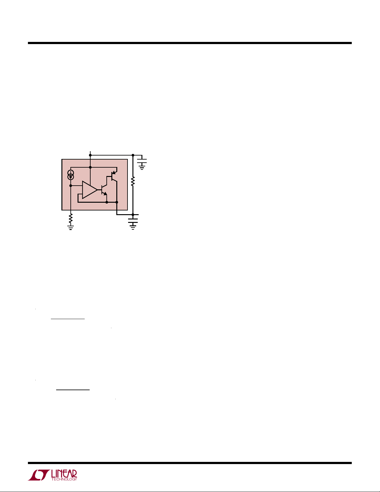
The second technique for reducing power dissipation,
shown in Figure 13, uses a resistor in parallel with the
LT3081. This resistor provides a parallel path for current
flow, reducing the current flowing through the LT3081.
This technique works well if input voltage is reasonably
constant and output load current changes are small. This
technique also increases the maximum available output
current at the expense of minimum load requirements.
LT3081
dissipates 1.52W of power. As with the first technique,
R
P
choose appropriate wattage resistors to handle and dissipate the
LT3081
increase by 0.64A to a total output current of 2.14A while
keeping the LT3081 in its normal operating range.
High Temperature Operation
power properly. With this configuration, the
supplies only 0.86A. Therefore, load current can
V
IN
50µA
+
–
R
SET
= 3.2V, I
= 3.65Ω
IN
OUT(MAX)
IN(MAX)
= 1.5A and I
carries no more than 90%
P
LT3081
SET OUT
Figure 13. Reducing Power Dissipation Using a Parallel Resistor
As an example, assume: VIN = 5V, V
= 3.3V, V
OUT(MIN)
= 0.7A. Also, assuming that R
of I
OUT(MIN)
Calculating R
= 630mA.
yields:
P
RP=
R
P
3081 F13
V
OUT
C2
C1
= 5.5V, V
OUT(MIN)
OUT
(5% Standard value = 3.6Ω)
The maximum total power dissipation is:
(5.5V – 3.2V) • 1.5A = 3.5W
However, the LT3081 supplies only:
1.5A –
= 0.86A
Therefore, the LT3081’s power dissipation is only:
P
= (5.5V – 3.2V) • 0.86A = 1.98W
DISS
Care must be taken when designing the LT3081H/
LT3081MP applications to operate at high ambient tem
peratures. The LT3081
H/LT3081MP operates at high
-
temperatures, but erratic operation can occur due to un-
in
foreseen variations
external components. Some tantalum
capacitors are available for high temperature operation, but
ESR is often several ohms; capacitor ESR above 0.5Ω is
unsuitable for use with the LT3081H/LT3081MP. Multiple
ceramic capacitor manufacturers
now offer
ceramic capaci-
tors that are rated to 150°C using an X8R dielectric. Check
passive component for absolute value and voltage
each
ratings over the operating temperature range.
Leakages in capacitors or from solder flux left after insuf
ficient board cleaning adversely affects low current nodes,
such
as the SET, I
, and TEMP pins. Consider junction
MON
temperature increase due to power dissipation in both
the junction and nearby components to ensure maximum
specifications are not violated for the LT3081H/LT3081MP
or external components.
Protection Features
The LT3081 incorporates several protection features ideal
for harsh industrial and automotive environments, among
other applications. In addition to normal monolithic regula
tor protection features such as current limiting and thermal
limiting, the LT3081 protects itself against reverse-input
voltages, reverse-output voltages, and large OUT-to-SET
pin voltages.
Current limit protection and thermal overload protection
protect the IC against output current overload conditions.
For normal operation, do not exceed the rated absolute
maximum junction temperature. The thermal shutdown
circuit’s temperature threshold is typically 165°C and
incorporates about 5°C of hysteresis.
For more information www.linear.com/LT3081
3081fc
21
Page 22
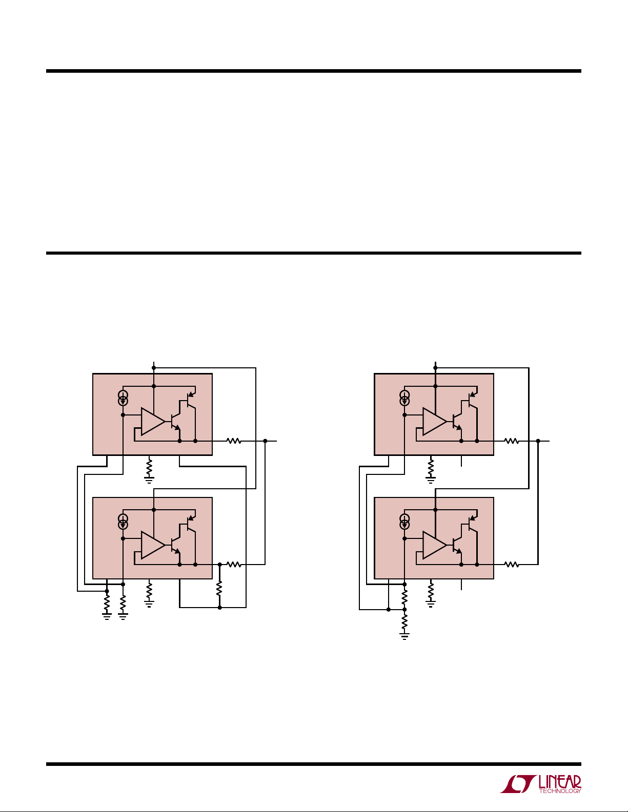
LT3081
applicaTions inForMaTion
The LT3081’s IN pin withstands ±40V voltages with respect
to the OUT and SET pins. Reverse current flow, if OUT is
greater than IN, is less than 1mA (typically under 100µA),
protecting the LT3081 and sensitive loads.
Clamping diodes and 400Ω limiting resistors protect the
LT3081’s SET pin relative to the OUT pin voltage. These
protection components typically only carry current under
transient overload conditions. These devices are sized to
Typical applicaTions
Paralleling Regulators Using I
V
IN
SET
I
SET
50µA
+
–
TEMP
IN
10mΩ
OUT
I
LIM
1k
V
OUT
3V
3A
LT3081
I
MON
handle ±10V differential voltages and ±25mA crosspin
current flow without concern. Relative to these applica
,
tion concerns
scenario employs
note the following two scenarios. The first
a noise-reducing SET pin bypass ca-
-
pacitor while OUT is instantaneously shorted to GND. The
second
scenario follows improper shutdown techniques
in which the SET pin is reset to GND quickly while OUT
is held up by a large output capacitance with light load.
Cancels Ballast Resistor Drop
MON
V
IN
SET
I
SET
50µA
+
–
TEMP
IN
R
BALLAST
10mΩ
OUT
I
LIM
1k
V
OUT
1.5V
3A
LT3081
I
MON
22
LT3081
I
MON
1k
I
SET
50µA
+
–
SET1kTEMP
R
SET
30.1k
IN
LT3081
I
SET
50µA
IN
+
R
10mΩ
OUT
I
LIM
3.01k
3081 TA03
I
MON
–
SET1kTEMP
R
SET
15k
R
COMP
25Ω
I
LIM
For more information www.linear.com/LT3081
OUT
BALLAST
10mΩ
3081 TA04
3081fc
Page 23
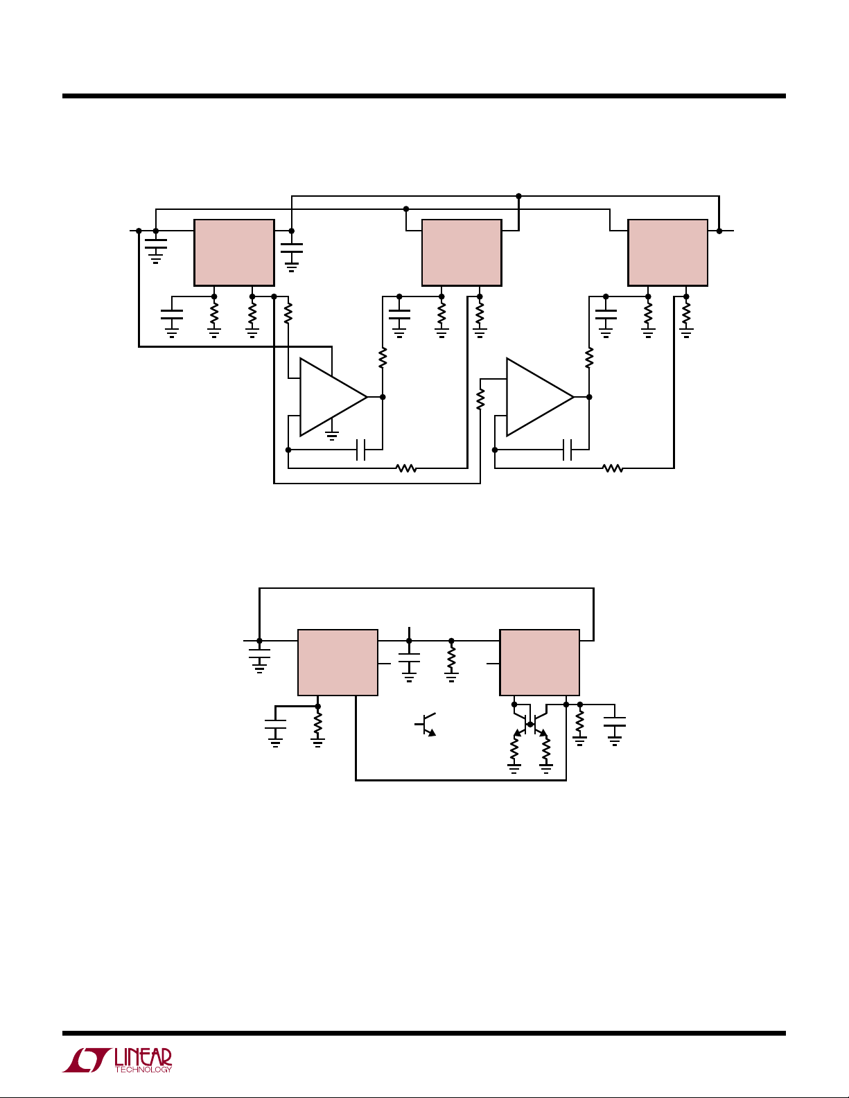
Typical applicaTions
V
3V TO 18V
IN
22µF
IN
OUT
LT3081
Load Sharing Without Ballast Resistors
IN
22µF
OUT
LT3081
IN OUT
LT3081
LT3081
V
OUT
1V
4.5A
0.1µF
3V TO 36V
SET
20k
V
IN
I
MON
1k 5.1k
I
SET
MON
20k
0.1µF
100k
+
1/2 LT1638 1/2 LT1638
–
0.47µF
5.1k
Load Current Sharing Without Ballasting
V
OUT
1V
3A
IN
4.7µF
SET
LT3081
I
MON
OUT
I
LIM
2.2µF
100Ω
1k
+
5.1k
–
OUT IN
LT3081
I
LIM
I
MON
0.47µF
SET
100k
5.1k
0.1µF
SET
20k
I
MON
3081 TA05
1k
20k
0.1µF
For more information www.linear.com/LT3081
= 2N3904
20k
1k1k
3081 TA05
0.1µF
3081fc
23
Page 24
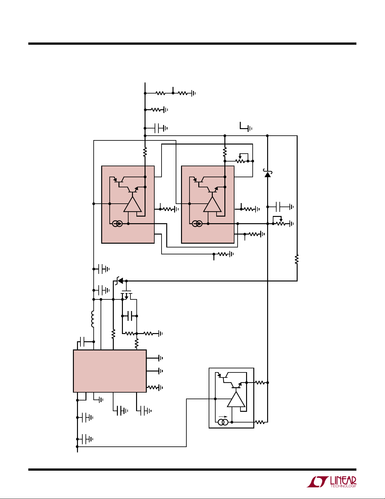
LT3081
Typical applicaTions
V
OUT
0V TO
20V
249Ω
22µF
9.09k
×2
ARDUINO
A1 PORT
1k
ARDUINO
GND PORT
CURRENT LIMIT 0A TO 3A
3081 TA07
10mΩ
OUT
LIM
I
IN
+
–
SET
I
50µA
LT3081
10µF
×2
6V
47µF
10nF
10µH
Constant-Voltage, Constant-Current 20V/3A Lab Supply
1µF
BSTV
SW
49.9k
BIAS
100k
1k
PG
TPO610T
FB
GND
SET TEMP
MON
I
4.99k
ARDUINO
A4 PORT
4.99k
IN
LT3081
10mΩ
5k
OUT
LIM
I
ARDUINO
+
–
SET
I
50µA
ARDUINO
SET TEMP
MON
I
10k
A2 PORT
ARDUINO
B140
0.01µF
A5 PORT
4.99k
10k
A3 PORT
×2
20k
10k
www.linear.com/product/LT3081#demoboards
24
LT8612
IN
EN/UV
SYNC
10µF
22µF
IN
V
30V
CC
INTV
1µF
PGND
RT
TR/SS
0.1µF
60.4k
IN
LT3092
10µA
+
–
49.9K 562Ω
SET OUT
3081fc
For more information www.linear.com/LT3081
Page 25
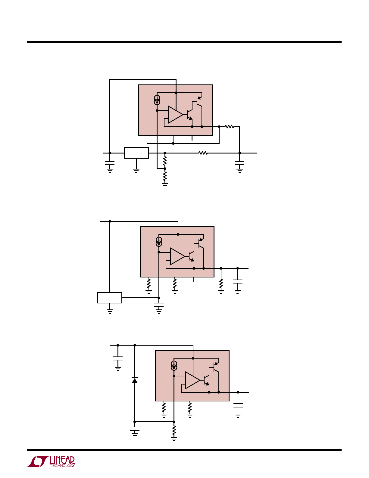
Typical applicaTions
LT3081
Boosting Fixed Output Regulators
V
5V
IN
INPUT
LT1019
GND
10µF
LT1963-3.3
OUTPUT
LT3081
I
MON
LT3081
I
MON
IN
I
SET
50µA
+
–
SET TEMP
8.2Ω*
6.2k
*4mV DROP ENSURES LT3081 IS OFF WITH NO LOAD
MULTIPLE LT3081s CAN BE USED
Reference Buffer
IN
I
SET
50µA
+
–
SET TEMP
1k 1k*1k
1µF
OUT
I
LIM
20mΩ
OUT
I
LIM
20mΩ
3081 TA08
47µF
*MIN LOAD 5mA
47µF
3.3V
OUT
3A
47µF
V
OUT
3081 TA09
V
4.8V TO 38V
Adding Soft-Start
IN
10µF
LT3081
IN4148
I
SET TEMP
MON
0.1µF
For more information www.linear.com/LT3081
I
SET
50µA
66.5k
IN
+
–
1k1k
OUT
I
LIM
10µF
V
OUT
3.3V
1.5A
3081 TA10
3081fc
25
Page 26
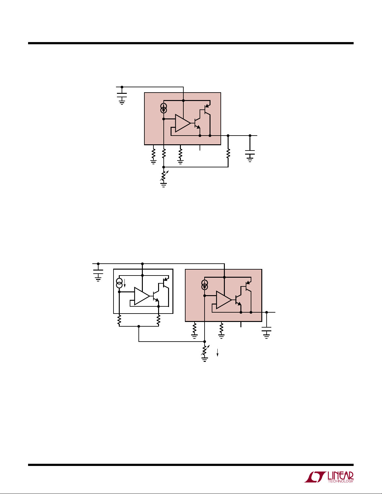
LT3081
Typical applicaTions
V
IN
12V
4.7µF
Using a Lower Value Set Resistor
I
SET
50µA
IN
LT3081
+
I
MON
–
SET1kTEMP
I
OUT
LIM
V
OUT
0.2V TO 10V
1k 4.02k 40.2Ω
R
SET
2k
V
= 0.2V + 5mA • R
OUT
4.7µF
3081 TA11
SET
Using an External Reference Current
V
IN
1µF
LT3092
SET OUT
20k 215Ω
10µA
IN
LT3081
+
–
I
SET1kTEMP
MON
1k
I
SET
50µA
IN
+
–
OUT
I
LIM
V
OUT
0V TO 20V
1µF
3081 TA12
26
20k
1mA
For more information www.linear.com/LT3081
3081fc
Page 27
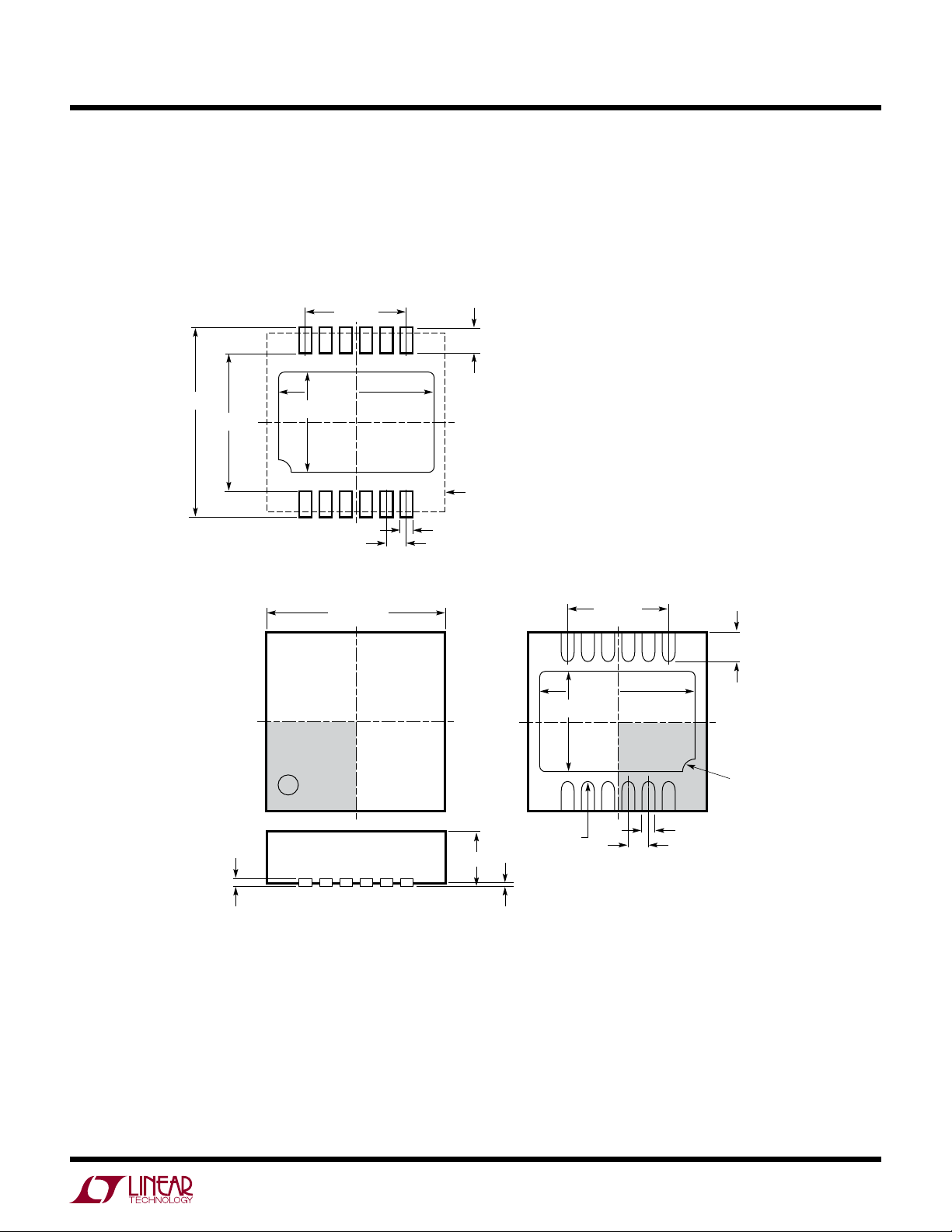
package DescripTion
Please refer to http://www.linear.com/designtools/packaging/ for the most recent package drawings.
DF Package
12-Lead Plastic DFN (4mm × 4mm)
(Reference LTC DWG # 05-08-1733 Rev A)
2.50 REF
0.70 ±0.05
LT3081
4.50 ±0.05
3.10 ±0.05
3.38 ±0.05
2.65 ±0.05
0.25 ±0.05
0.50 BSC
RECOMMENDED SOLDER PAD PITCH AND DIMENSIONS
APPLY SOLDER MASK TO AREAS THAT ARE NOT SOLDERED
4.00 ±0.10
(4 SIDES)
PIN 1
TOP MARK
(NOTE 6)
0.200 REF
0.75 ±0.05
PACKAGE OUTLINE
R = 0.115
2.50 REF
3.38 ±0.10
2.65 ±0.10
16
TYP
BOTTOM VIEW—EXPOSED PAD
127
0.25 ±0.05
0.50 BSC
0.40 ±0.10
PIN 1 NOTCH
R = 0.20 TYP OR
0.35 × 45°
CHAMFER
(DF12) DFN 1112 REV A
NOTE:
0.00 – 0.05
1. PACKAGE OUTLINE DOES NOT CONFORM TO JEDEC MO-229
2. DRAWING NOT TO SCALE
3. ALL DIMENSIONS ARE IN MILLIMETERS
4. DIMENSIONS OF EXPOSED PAD ON BOTTOM OF PACKAGE DO NOT INCLUDE
MOLD FLASH. MOLD FLASH, IF PRESENT, SHALL NOT EXCEED 0.15mm ON ANY SIDE
5. EXPOSED PAD SHALL BE SOLDER PLATED
6. SHADED AREA IS ONLY A REFERENCE FOR PIN 1 LOCATION
ON THE TOP AND BOTTOM OF PACKAGE
For more information www.linear.com/LT3081
3081fc
27
Page 28
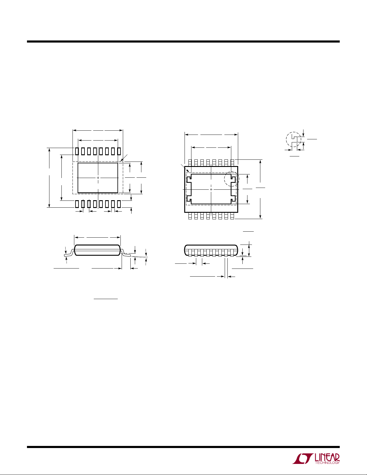
LT3081
package DescripTion
Please refer to http://www.linear.com/designtools/packaging/ for the most recent package drawings.
FE Package
16-Lead Plastic TSSOP (4.4mm)
(Reference LTC DWG # 05-08-1663 Rev K)
Exposed Pad Variation BB
4.70
(.185)
3.58
(.141)
6.60 ±0.10
4.50 ±0.10
RECOMMENDED SOLDER PAD LAYOUT
0.09 – 0.20
(.0035 – .0079)
NOTE:
1. CONTROLLING DIMENSION: MILLIMETERS
2. DIMENSIONS ARE IN
3. DRAWING NOT TO SCALE
4. RECOMMENDED MINIMUM PCB METAL SIZE
FOR EXPOSED PAD ATTACHMENT
SEE NOTE 4
0.65 BSC
4.30 – 4.50*
(.169 – .177)
0.45 ±0.05
0.50 – 0.75
(.020 – .030)
MILLIMETERS
(INCHES)
NOTE 5
2.94
(.116)
1.05 ±0.10
0.25
REF
4.90 – 5.10*
(.193 – .201)
3.58
(.141)
16 1514 13 12 11
NOTE 5
3.05
(.120)
1 3 45678
2
0° – 8°
0.65
(.0256)
BSC
0.195 – 0.30
(.0077 – .0118)
TYP
5. BOTTOM EXPOSED PADDLE MAY HAVE METAL PROTRUSION
IN THIS AREA. THIS REGION MUST BE FREE OF ANY EXPOSED
TRACES OR VIAS ON PBC LAYOUT
*DIMENSIONS DO NOT INCLUDE MOLD FLASH. MOLD FLASH
SHALL NOT EXCEED 0.150mm (.006") PER SIDE
10 9
DETAIL A
0.05 – 0.15
(.002 – .006)
FE16 (BB) TSSOP REV K 0913
2.94
(.116)
1.10
(.0433)
MAX
DETAIL A IS THE PART OF THE
LEAD FRAME FEATURE FOR
REFERENCE ONLY
NO MEASUREMENT PURPOSE
6.40
(.252)
BSC
DETAIL A
0.56
(.022)
REF
0.53
(.021)
REF
28
3081fc
For more information www.linear.com/LT3081
Page 29
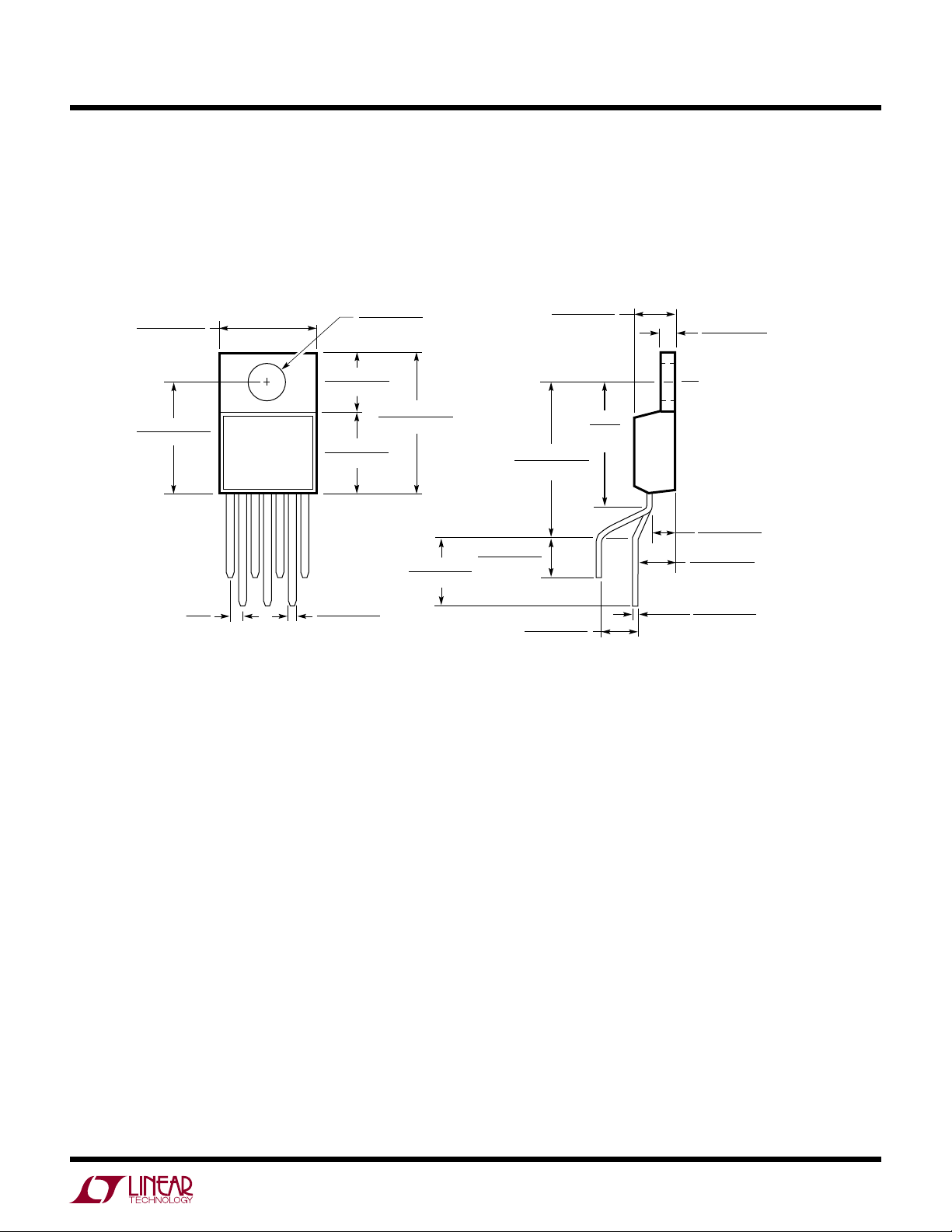
package DescripTion
T7 (TO-220) 0801
Please refer to http://www.linear.com/designtools/packaging/ for the most recent package drawings.
T7 Package
7-Lead Plastic TO-220 (Standard)
(Reference LTC DWG # 05-08-1422)
LT3081
.390 – .415
(9.906 – 10.541)
.460 – .500
(11.684 – 12.700)
.050
BSC
(1.27)
.147 – .155
(3.734 – 3.937)
.230 – .270
(5.842 – 6.858)
.330 – .370
(8.382 – 9.398)
.026 – .036
(0.660 – 0.914)
DIA
.570 – .620
(14.478 – 15.748)
.260 – .320
(6.604 – 8.128)
SEATING PLANE
.152 – .202
(3.860 – 5.130)
.165 – .180
(4.191 – 4.572)
.700 – .728
(17.780 – 18.491)
.135 – .165
(3.429 – 4.191)
.045 – .055
(1.143 – 1.397)
.620
(15.75)
TYP
.095 – .115
(2.413 – 2.921)
.155 – .195*
(3.937 – 4.953)
.013 – .023
(0.330 – 0.584)
*MEASURED AT THE SEATING PLANE
For more information www.linear.com/LT3081
3081fc
29
Page 30
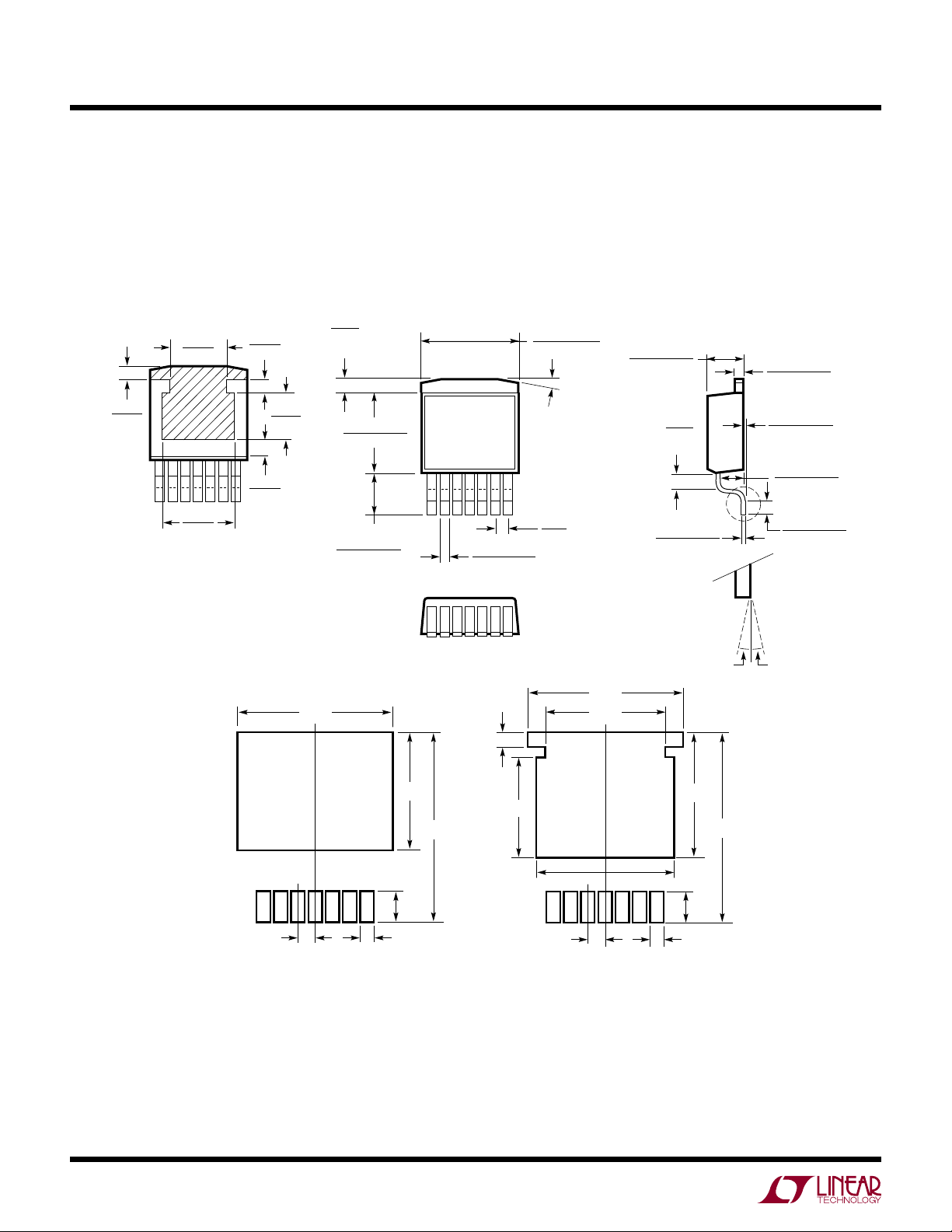
LT3081
package DescripTion
Please refer to http://www.linear.com/designtools/packaging/ for the most recent package drawings.
R Package
7-Lead Plastic DD Pak
(Reference LTC DWG # 05-08-1462 Rev F)
.256
(6.502)
.060
(1.524)
.300
(7.620)
BOTTOM VIEW OF DD PAK
HATCHED AREA IS SOLDER PLATED
COPPER HEAT SINK
.060
(1.524)
.075
(1.905)
.183
(4.648)
.060
(1.524)
( )
.420
TYP
.330 – .370
(8.382 – 9.398)
+.012
.143
–.020
+0.305
3.632
–0.508
.026 – .035
(0.660 – 0.889)
TYP
.080
.390 – .415
(9.906 – 10.541)
15° TYP
.050
(1.27)
BSC
.420
.276
.165 – .180
(4.191 – 4.572)
.059
(1.499)
TYP
.013 – .023
(0.330 – 0.584)
DETAIL A
DETAIL A
.045 – .055
(1.143 – 1.397)
+.008
.004
–.004
+0.203
0.102
( )
–0.102
.095 – .115
(2.413 – 2.921)
.050 ±.012
(1.270 ±0.305)
0° – 7° TYP0° – 7° TYP
30
.050
RECOMMENDED SOLDER PAD LAYOUT
NOTE:
1. DIMENSIONS IN INCH/(MILLIMETER)
2. DRAWING NOT TO SCALE
For more information www.linear.com/LT3081
.350
.090
.035
.585
.205
.320
RECOMMENDED SOLDER PAD LAYOUT
FOR THICKER SOLDER PASTE APPLICATIONS
.325
.090
.035.050
R (DD7) 0212 REV F
.585
3081fc
Page 31
LT3081
revision hisTory
REV DATE DESCRIPTION PAGE NUMBER
A 11/13 Modified Typical Application circuit for more detail
Added H- and MP-grade references
Changed T
Changed specs to TEMP Output Current Absolute Error
Modified Block Diagram
Modified Paralleling Regulators Circuit
Modified Arduino Supply Circuit
Added new Typical Application circuits
Modified High Efficiency Adjustable Supply circuit
Updated Related Parts Table
B 7/14 Updated the Typical Application circuit.
Changed T7 diagram to 'Standard’ package drawing.
C 3/15 Updated Typical Values for External I
Corrected I
Corrected Formula and Text in Programming Current Limit Section
to 150°C on the FE and T7 packages
JMAX
Programming
LIM
Text in Pin Functions
LIM
1
Throughout
2
4
10
22
24
25, 26
32
32
1
29
3
10
13
Information furnished by Linear Technology Corporation is believed to be accurate and reliable.
However, no responsibility is assumed for its use. Linear Technology Corporation makes no representation that the interconnection of its circuits as described herein will not infringe on existing patent rights.
For more information www.linear.com/LT3081
3081fc
31
Page 32
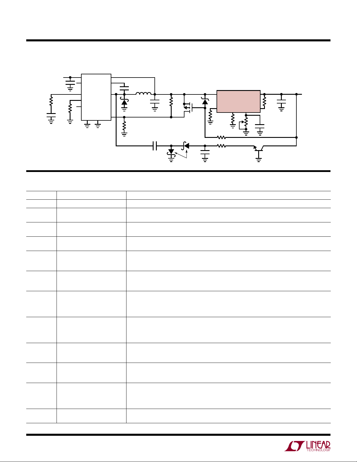
LT3081
Typical applicaTion
High Efficiency Adjustable Supply
V
6.3V TO
36V
15k
1000pF
IN
63.4k
V
IN
RUN/SS
LT3680
V
C
RT
PG
SYNC
GND
BOOST
SW
BD
0.47µF
6.8µH
MBRA340T3
FB
15k
relaTeD parTs
PART NUMBER DESCRIPTION COMMENTS
LT1185 3A Negative Low Dropout Regulator V
LT1764/
LT1764A
LT1963/
LT1963A
3A, Fast T
Low Noise LDO
1.5A Low Noise, Fast T
Response LDO
ransient Response,
ransient
LT1965 1.1A, Low Noise, Low Dropout
Linear Regulator
LT3022 1A, Low Voltage, VLDO Linear
Regulator
LT3070 5A, Low Noise, Programmable
V
, 85mV Dropout Linear
OUT
Regulator with Digital Margining
LT3071 5A, Low Noise, Programmable
V
, 85mV Dropout Linear
OUT
Regulator with Analog Margining
LT3080/
LT3080-1
1.1A, Parallelable, Low Noise,
Low Dropout Linear Regulator
LT3082 200mA, Parallelable, Single
Resistor, Low Dropout Linear
Regulator
LT3085 500mA, Parallelable, Low Noise,
Low Dropout Linear Regulator
LT3092
200mA 2-Terminal Programmable
Current Source
LT3083 Adjustable 3A Single Resistor
Low Dropout Regulator
: –4.5V to –35V, 0.8V Dropout Voltage, DD-Pak and TO-220 Packages
IN
340mV Dropout Voltage, Low Noise: 40µV
LT1764A Version Stable Also with Ceramic Capacitors
340mV Dropout Voltage, Low Noise: 40µV
Ceramic Capacitors, TO-220, DD, TSSOP, SOT-223 and SO-8 Packages
290mV Dropout Voltage, Low Noise: 40µV
Ceramic Capacitors, TO-220, DD-Pak, MSOP and 3mm × 3mm DFN Packages
: 0.9V to 10V, Dropout Voltage: 145mV Typical, Adjustable Output (V
V
IN
Stable with Low ESR, Ceramic Output Capacitors, 16-Pin DFN (5mm × 3mm) and 16-Lead
MSOP Packages
Dropout Voltage: 85mV, Digitally Programmable V
±3% or ±5%, Low Output Noise: 25µV
Stable with Low ESR Ceramic Output Capacitors (15µF Minimum), 28-Lead 4mm × 5mm QFN Package
Dropout Voltage: 85mV, Digitally Programmable V
Low Output Noise: 25µV
Current Monitor, Stable with Low ESR Ceramic Output Capacitors (15µF Minimum) 28-Lead
4mm × 5mm QFN Package
300mV
Dropout Voltage (2-Supply Operation), Low Noise: 40µV
Current-Based Reference
Stable with Ceramic Capacitors, TO-220, DD-Pak, SOT-223, MS8E and 3mm × 3mm DFN-8 Packages;
LT3080-1 Version Has Integrated Internal Ballast Resistor
Outputs May Be Paralleled for Higher Output, Current or Heat Spreading, Wide Input Voltage
Range: 1.2V to 40V Low Value Input/Output Capacitors Required: 2.2µF, Single Resistor Sets Output
Voltage 8-Lead SOT-23, 3-Lead SOT-223 and 8-Lead 3mm × 3mm DFN Packages
275mV
Dropout Voltage (2-Supply Operation), Low Noise: 40µV
V
: 0V to 35.7V, Current-Based Reference with 1-Resistor V
OUT
(No Op Amp Required), Stable with Ceramic Capacitors, MS8E and 2mm × 3mm DFN-6 Packages
Programmable 2-Terminal Current Source, Maximum Output Current = 200mA, Wide Input Voltage
Range: 1.2V to 40V, Resistor Ratio Sets Output Current, Initial Set Pin Current Accuracy = 1%, Current
Limit and Thermal Shutdown Protection, Reverse-Voltage Protection, Reverse-Current Protection,
8-Lead SOT-23, 3-Lead SOT-223 and 8-Lead 3mm × 3mm DFN Packages.
Low Noise: 40µV
(DD-Pak and TO-220), Low Dropout Operation: 310mV (2 Supplies)
IN OUT
47µF
590k
MTD2955
1µF
CMDSH-4E
(10Hz to 100kHz), Parallelable: Use Tw o for a 10A Output, I
RMS
with 1-Resistor V
, 50µA Set Pin Current, Output Adjustable to 0V, Wide Input Voltage Range: 1.2V to 23V
RMS
6V
1k
1µF
RMS
RMS
RMS
(10Hz to 100kHz), Parallelable: Use Tw o for a 10A Output,
RMS
OUT
LT3081
TEMP SET
I
MON
1k
10k
1k
, VIN = 2.7V to 20V, TO-220, TSSOP and DD-Pak,
, VIN = 2.5V to 20V, LT1963A Version Stable with
, VIN: 1.8V to 20V, V
: 0.8V to 1.8V, Digital Output Margining: ±1%,
OUT
: 0.8V to 1.8V, Analog Margining: ±10%,
OUT
Set; Directly Parallelable (No Op Amp Required),
6.04k
I
LIM
500k
0.1µF
2N3904
: 1.2V to 19.5V, Stable with
OUT
REF
, VIN: 1.2V to 36V, V
RMS
, VIN: 1.2V to 36V,
RMS
Set; Directly Parallelable
OUT
= V
22µF
3081 TA13
OUT(MIN)
V
OUT
0V TO
25V,
1.5A
= 200mV),
Output
MON
: 0V to 35.7V,
OUT
32
Linear Technology Corporation
1630 McCarthy Blvd., Milpitas, CA 95035-7417
(408) 432-1900 ● FAX: (408) 434-0507
For more information www.linear.com/LT3081
●
www.linear.com/LT3081
3081fc
LT 0315 REV C • PRINTED IN USA
LINEAR TECHNOLOGY CORPORATION 2014
 Loading...