

Page 1
FEATURES
LT1949
600kHz, 1A Switch
PWM DC/DC Converter
U
DESCRIPTIO
■
1A, 0.5Ω, 30V Internal Switch
■
Operates with VIN as Low as 1.5V
■
600kHz Fixed Frequency Operation
■
Low-Battery Detector Stays Active in Shutdown
■
Low V
■
Pin-for-Pin Compatible with the LT1317B
■
Small 8-Lead MSOP and SO Packages
Switch: 410mV at 800mA
CESAT
U
APPLICATIO S
■
LCD Bias Supplies
■
GPS Receivers
■
Battery Backup
■
Portable Electronic Equipment
■
Diagnostic Medical Instrumentation
U
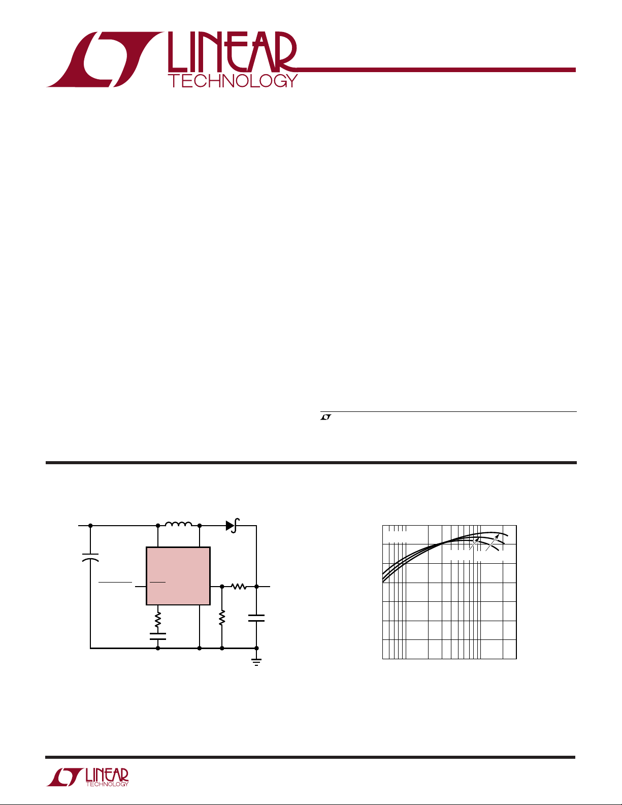
TYPICAL APPLICATIO
The LT®1949 is a fixed frequency step-up DC/DC converter with a 1A, 0.5Ω internal switch. Capable of generating 10V at 175mA from a 3.3V input, the LT1949 is ideal
for generating bias voltages for large screen LCD panels.
Constant frequency 600kHz operation results in a low
noise output that is easy to filter and the 30V switch rating
allows output voltage up to 28V using a single inductor. An
external compensation pin gives the user flexibility in
optimizing loop compensation, allowing small low ESR
ceramic capacitors to be used at the output. The 8-lead
MSOP and SO packages ensure a low profile overall
solution.
The LT1949 includes a low-battery detector that stays
alive when the device goes into shutdown. Quiescent
current in shutdown is 25µA, while operating current is
4.5mA.
, LTC and LT are registered trademarks of Linear Technology Corporation.
V
IN
3.3V
+
C1
22µF
C1: AVX TAJA226M006R
C2: TAIYO YUDEN LMK325BJ106MN
D1: MBRM120LT3
L1: SUMIDA CDRH62B-100
L1
10µH
V
IN
SHDNSHUTDOWN
V
C
68k
SW
LT1949
GND
330pF
D1
R1
FB
1M
R2
140k
V
OUT
10V
175mA
C2
10µF
CERAMIC
1949 F01
90
V
= 10V
OUT
80
70
60
50
EFFICIENCY (%)
40
30
20
5 10050 300
10
LOAD CURRENT (mA)
3.6V
4.2V
IN
IN
Figure 1. 3.3V to 10V/175mA DC/DC Converter Figure 2. 3.3V to 10V Converter Efficiency
3V
1949 F02
IN
1
Page 2
LT1949
WWWU
ABSOLUTE AXI U RATI GS
(Note 1)
VIN, LBO Voltage..................................................... 12V
SW Voltage ............................................... –0.4V to 30V
FB Voltage .................................................... VIN + 0.3V
VC Voltage ................................................................ 2V
LBI Voltage ............................................ 0V ≤ V
LBI
≤ 1V
SHDN Voltage ........................................................... 6V
UU
W
PACKAGE/ORDER I FOR ATIO
ORDER PART
TOP VIEW
V
1
C
2
FB
3
SHDN
4
GND
MS8 PACKAGE
8-LEAD PLASTIC MSOP
T
= 125°C, θJA = 120°C/W
JMAX
Consult factory for Military grade parts.
8
LBO
7
LBI
6
V
IN
5
SW
NUMBER
LT1949EMS8
MS8 PART MARKING
LTJC
Junction Temperature.......................................... 125°C
Operating Temperature Range (Note 2)
LT1949EMS8.......................................–40°C to 85°C
LT1949ES8/LT1949IS8 .......................–40°C to 85°C
Storage Temperature ........................... – 65°C to 150°C
Lead Temperature (Soldering, 10sec).................. 300°C
ORDER PART
NUMBER
LT1949ES8
LT1949IS8
S8 PART MARKING
1949E
1949I
SHDN
GND
V
1
C
FB
2
3
4
T
JMAX
8-LEAD PLASTIC SO
TOP VIEW
8
7
6
5
S8 PACKAGE
= 125°C, θJA = 120°C/W
LBO
LBI
V
SW
IN
ELECTRICAL CHARACTERISTICS
temperature range, otherwise specifications are TA = 25°C. VIN = 2V, V
SYMBOL PARAMETER CONDITIONS MIN TYP MAX UNITS
I
V
I
g
A
f
Q
FB
B
m
V
OSC
Quiescent Current ● 4.5 7.5 mA
Feedback Voltage 1.22 1.24 1.26 V
FB Pin Bias Current (Note 3) ● 12 80 nA
Input Voltage Range ● 1.7 12 V
Error Amp Transconductance ∆I = 5µA ● 70 140 240 µmhos
Error Amp Voltage Gain 700 V/V
Maximum Duty Cycle ● 80 85 %
Switch Current Limit (Note 4) VIN = 2.5V, Duty Cycle = 30% 1 1.13 1.5 A
Switching Frequency ● 500 600 750 kHz
Shutdown Pin Current V
LBI Threshold Voltage 190 200 210 mV
LBO Output Low I
LBO Leakage Current V
LBI Input Bias Current (Note 5) V
Low-Battery Detector Gain 1MΩ Pull-Up 2000 V/V
Switch Leakage Current VSW = 5V ● 0.01 3 µA
The ● denotes specifications which apply over the full operating
= 2V unless otherwise noted.
SHDN
V
= 0V ● 25 40 µA
SHDN
● 1.20 1.24 1.26 V
V
= 2.5V, Duty Cycle = 30% ● 0.95 1.5 A
IN
= V
SHDN
IN
= 0V ● –2.3 – 7 µA
V
SHDN
= 10µA ● 0.15 0.25 V
SINK
= 250mV, V
LBI
= 150mV ● 560nA
LBI
= 5V ● 0.02 0.1 µA
LBO
● 0.015 0.1 µA
● 180 200 220 mV
2
Page 3

LT1949
TEMPERATURE (°C)
–50
SWITCH CURRENT (A)
1.3
1.2
1.1
1.0
0.9
0.8
–25
02550
1949 G03
75 100
TEMPERATURE (°C)
–50 –25
QUIESCENT CURRENT (mA)
1949 G06
4.6
4.5
4.4
4.3
4.2
4.1
4.0
3.9
3.8
0 255075100
ELECTRICAL CHARACTERISTICS
temperature range, otherwise specifications are TA = 25°C. VIN = 2V, V
The ● denotes specifications which apply over the full operating
= 2V unless otherwise noted.
SHDN
SYMBOL PARAMETER CONDITIONS MIN TYP MAX UNITS
Switch V
CESAT
ISW = 800mA 410 mV
= 500mA ● 400 mV
I
SW
Reference Line Regulation 1.8V ≤ VIN ≤ 12V ● 0.08 0.15 %/V
SHDN Input Voltage High ● 1.4 6 V
SHDN Input Voltage Low ● 0.4 V
Note 1: Absolute Maximum Ratings are those values beyond which the life
of a device may be impaired.
Note 2: The LT1949E is guaranteed to meet performance specifications
from 0°C to 70°C. Specifications over the –40°C to 85°C operating
Note 3: Bias current flows into FB pin.
Note 4: Switch current limit guaranteed by design and/or correlation to
static tests. Duty cycle affects current limit due to ramp generator.
Note 5: Bias current flows out of LBI pin.
temperature range are assured by design, characterization and correlation
with statistical process controls.
UW
TYPICAL PERFOR A CE CHARACTERISTICS
Switch Current Limit,
Oscillator Frequency
700
Switch Current Limit
1.3
Duty Cycle = 30%
650
600
550
OSCILLATOR FREQUENCY (kHz)
500
0
Switch Voltage Drop (V
1.0
0.8
0.6
0.4
SWITCH VOLTAGE (V)
0.2
0
0
–40°C
25°C
85°C
2468
INPUT VOLTAGE
CESAT
25°C
–40°C
0.4 0.6 0.8
0.2
SWITCH CURRENT (A)
10 12
1949 G01
)
85°C
1.0 1.2
1949 G04
1.2
1.1
1.0
SWITCH CURRENT (A)
0.9
0.8
20
0
Feedback Voltage
1.25
1.24
1.23
1.22
FEEDBACK VOLTAGE (V)
1.21
1.20
–50
–25 0 25 50
60
40
DUTY CYCLE (%)
TEMPERATURE (°C)
80
1949 G02
75 100
1949 G05
100
Quiescent Current, SHDN = 2V
3
Page 4

LT1949
UW
TYPICAL PERFOR A CE CHARACTERISTICS
Quiescent Current, SHDN = 0V
26
25
24
23
22
QUIESCENT CURRENT (µA)
21
20
–25 0 25 50
–50
TEMPERATURE (°C)
Load Regulation
V
OUT
50mV/DIV
DC
COUPLED
OFFSET
ADDED
I
= 3V
V
IN
V
= 10V
OUT
L1 = 10µH, SUMIDA CD54
= 10µF CERAMIC 1949 G10
C
OUT
LOAD
25mA/DIV
75 100
1317 TPC10
FB Pin Bias Current
40
36
32
28
24
20
16
12
FB PIN BIAS CURRENT (nA)
8
4
0
–50 –25 0 25 50 75 100
TEMPERATURE (°C)
Load Regulation
V
OUT
50mV/DIV
DC
COUPLED
OFFSET
ADDED
50mA/DIV
I
= 4V
V
IN
= 10V
V
OUT
L1 = 10µH, SUMIDA CD54
C
= 10µF CERAMIC 1949 G11
OUT
LOAD
1317 TPC11
–1
SHDN PIN CURRENT (µA)
–2
–3
V
OUT
100mV/DIV
AC COUPLED
500mA/DIV
200mA
I
LOAD
100mA
SHDN Pin Current
2
1
0
12 4
0
SHDN PIN VOLTAGE (V)
Transient Response
I
L
V
= 3.3V
IN
= 10V
V
OUT
CIRCUIT OF FIGURE 1
3
50µs/DIV
1949 G12
5
1317 TPC12
6
U
UU
PI FU CTIO S
VC (Pin 1): Compensation Pin for Error Amplifier. Connect a series RC network from this pin to ground. Typical
values for compensation are a 68k/330pF combination
when using ceramic output capacitors. Minimize trace
area at VC.
FB (Pin 2): Feedback Pin. Reference voltage is 1.24V.
Connect resistor divider tap here. Minimize trace area at
FB. Set V
according to: V
OUT
= 1.24V(1 + R1/R2).
OUT
SHDN (Pin 3): Shutdown. Pull this pin low for shutdown
mode (only the low-battery detector remains active).
Leave this pin floating or tie to a voltage between 1.4V and
6V to enable the device. SHDN pin is logic level and need
only meet the logic specification (1.4V for high, 0.4V for
low).
4
GND (Pin 4): Ground. Connect directly to local ground
plane.
SW (Pin 5): Switch Pin. Connect inductor/diode here.
Minimize trace area at this pin to keep EMI down.
VIN (Pin 6): Supply Pin. Must be bypassed close to the
pin.
LBI (Pin 7):
Low-Battery Detector Input. 200mV reference. Voltage on LBI must stay between ground and
700mV. Low-battery detector remains active in shutdown
mode.
LBO (Pin 8): Low-Battery Detector Output. Open collector, can sink 10µA. A 1MΩ pull-up is recommended.
Page 5

BLOCK DIAGRA
LT1949
W
1.24V
REFERENCE
V
OUT
R1
(EXTERNAL)
R2
(EXTERNAL)
LBI
200mV
R
7
+
–
A4
SHUTDOWN
FF
Q
S
DRIVER
LBO
8
SHDN
3
SW
5
Q3
+
A = 2
0.06Ω
–
4
1949 BD
GND
+
g
–
m
ERROR
AMPLIFIER
FB
2
FB
BIAS
V
C
1
+
–
ENABLE
A1
COMPARATOR
–
RAMP
GENERATOR
600kHz
OSCILLATOR
+
Σ
+
+
A2
COMPARATOR
Figure 3. LT1949 Block Diagram
U
OPERATIO
The LT1949 is a current mode, fixed frequency step-up
DC/DC converter with an internal 1A NPN power transistor. Operation can best be understood by referring to the
Block Diagram.
At the beginning of each oscillator cycle, the flip-flop is set
and the switch is turned on. Current in the switch ramps
up until the voltage at A2’s positive input reaches the V
pin voltage, causing A2’s output to change state and the
switch to be turned off. The signal at A2’s positive input is
a summation of a signal representing switch current and
a ramp generator (introduced to avoid subharmonic oscillations at duty factors greater than 50%). If the load
increases, V
(and FB) will drop slightly and the error
OUT
amplifier will drive VC to a higher voltage, causing current
in the switch to increase. In this way, the error amplifier
drives the VC pin to the voltage necessary to satisfy the
load. Frequency compensation is provided by an external
series RC network connected between the VC pin and
ground.
C
Layout Hints
The LT1949 switches current at high speed, mandating
careful attention to layout for proper performance.
You
will not get advertised performance with careless layouts.
Figure 4 shows recommended component placement for
a boost (step-up) converter. Follow this closely in your PC
layout. Note the direct path of the switching loops. Input
capacitor C1
must
be placed close (<5mm) to the IC
package. As little as 10mm of wire or PC trace from CIN to
VIN will cause problems such as inability to regulate or
oscillation.
The ground terminal of output capacitor C2 should tie
close to Pin 4 of the LT1949. Doing this reduces dI/dt in the
ground copper which keeps high frequency spikes to a
minimum. The DC/DC converter ground should tie to the
PC board ground plane at one place only, to avoid introducing dI/dt in the ground plane.
5
Page 6

LT1949
OPERATIO
U
GROUND PLANE
LBI
LBO
C1
+
V
IN
R1
R2
SHUTDOWN
MULTIPLE
VIAs
GND
Figure 4. Recommended Component Placement for Boost
Converter. Note Direct High Current Paths Using Wide PC
Traces. Minimize Trace Area at Pin 1 (VC) and Pin 2 (FB).
Use Multiple Vias to Tie Pin 4 Copper to Ground Plane. Use
Vias at One Location Only to Avoid Introducing Switching
Currents into the Ground Plane
U
WUU
APPLICATIONS INFORMATION
Low-Battery Detector
1
2
LT1949
3
4
C2
8
7
6
5
V
OUT
L1
1949 F04
The LT1949’s low-battery detector is a simple PNP input
gain stage with an open collector NPN output. The negative input of the gain stage is tied internally to a 200mV
±5% reference. The positive input is the LBI pin. Arrangement as a low-battery detector is straightforward.
3.3V
R1
LBI
R2
100k
+
–
200mV
INTERNAL
REFERENCE
GND
V
LT1949
IN
LBO
1949 F05
1M
R1 =
TO PROCESSOR
V
– 200mV
LB
2µA
Figure 5. Setting Low-Battery Detector Trip Point
6
Figure␣ 5 details hookup. R1 and R2 need only be low
enough in value so that the bias current of the LBI pin
doesn’t cause large errors. For R2, 100k is adequate. The
200mV reference can also be accessed as shown in
Figure␣ 6. The low-battery detector remains active in
shutdown.
200k
2N3906
V
REF
200mV
10k
+
10µF
Figure 6. Accessing 200mV Reference
LBO
LBI
V
IN
LT1949
GND
1949 F06
Page 7

TYPICAL APPLICATIO
V
IN
4V TO 9V
PACKAGE DESCRIPTIO
U
4 Cell to 5V SEPIC Converter
C2
SW
GND
4.7µF
16V
FB
L2
10µH
D1
1M
1%
332k
1%
C1
4.7µF
16V
1M
1M
V
IN
SHDN
V
C
L1
10µH
LT1949
33k
3.3nF
U
Dimensions in inches (millimeters) unless otherwise noted.
LT1949
V
OUT
5V
250mA
C3
10µF
6.3V
C1, C2: TAIYO YUDEN EMK316BJ475ML
C3: TAIYO YUDEN JMK316BJ106ML
D1: MOTOROLA MBRM120LT3
L1, L2: SUMIDA CR32-100KC
1949 TA02
0.007
(0.18)
0.021
± 0.006
(0.53 ± 0.015)
* DIMENSION DOES NOT INCLUDE MOLD FLASH, PROTRUSIONS OR GATE BURRS. MOLD FLASH,
PROTRUSIONS OR GATE BURRS SHALL NOT EXCEED 0.006" (0.152mm) PER SIDE
** DIMENSION DOES NOT INCLUDE INTERLEAD FLASH OR PROTRUSIONS.
INTERLEAD FLASH OR PROTRUSIONS SHALL NOT EXCEED 0.006" (0.152mm) PER SIDE
0.010 – 0.020
(0.254 – 0.508)
0.008 – 0.010
(0.203 – 0.254)
*
DIMENSION DOES NOT INCLUDE MOLD FLASH. MOLD FLASH
SHALL NOT EXCEED 0.006" (0.152mm) PER SIDE
**
DIMENSION DOES NOT INCLUDE INTERLEAD FLASH. INTERLEAD
FLASH SHALL NOT EXCEED 0.010" (0.254mm) PER SIDE
×
°
45
0.016 – 0.050
(0.406 – 1.270)
° – 6° TYP
0
0°– 8° TYP
MS8 Package
8-Lead Plastic MSOP
(LTC DWG # 05-08-1660)
0.040
SEATING
PLANE
± 0.006
(1.02 ± 0.15)
0.012
(0.30)
0.0256
REF
(0.65)
BSC
0.034 ± 0.004
(0.86 ± 0.102)
0.006 ± 0.004
(0.15 ± 0.102)
S8 Package
8-Lead Plastic Small Outline (Narrow 0.150)
(LTC DWG # 05-08-1610)
0.053 – 0.069
(1.346 – 1.752)
0.014 – 0.019
(0.355 – 0.483)
TYP
0.004 – 0.010
(0.101 – 0.254)
0.050
(1.270)
BSC
0.118 ± 0.004*
(3.00 ± 0.102)
0.193 ± 0.006
(4.90 ± 0.15)
0.228 – 0.244
(5.791 – 6.197)
8
12
0.189 – 0.197*
(4.801 – 5.004)
7
8
1
2
7
6
3
5
0.118 ± 0.004**
(3.00 ± 0.102)
MSOP (MS8) 1098
4
5
6
3
4
0.150 – 0.157**
(3.810 – 3.988)
SO8 1298
Information furnished by Linear Technology Corporation is believed to be accurate and reliable.
However, no responsibility is assumed for its use. Linear Technology Corporation makes no representation that the interconnection of its circuits as described herein will not infringe on existing patent rights.
7
Page 8

LT1949
TYPICAL APPLICATIO
U
Low Profile Triple Output LCD Bias Generator
L1
SHDNSHUTDOWN
LBI
LB0
10µH
V
IN
LT1949
V
C
R1
47k
C3
680pF
V
IN
3.3V
+
C1
22µF
C1: AVX TAJB226M010
C2: TAIYO YUDEN TMK432BJ106MN X7R 1210
C4, C5, C6: TAIYO YUDEN LMK316BJ475ML X5R1206
C7, C8, C9: 0.1µF CERAMIC, 50V
D1 TO D6: FMMD7000, DUAL DIODE
D7: MBRM120LT3
L1: SUMIDA CDRH62B-100
SW
GND
FB
D1 D2
4.7µF
C7
0.1µF
D7
C6
C8
0.1µF
R2
40.2k
1%
R3
7.5k
1%
D5
D6
D3 D4
C9
0.1µF
C2
10µF
C5
4.7µF
1949 TA01
23V
5mA
8V
200mA
C4
4.7µF
–8V
10mA
RELATED PARTS
PART NUMBER DESCRIPTION COMMENTS
LT1054 High Power Regulated Charge Pump Up to 100mA Output with No Inductors
LT1302 High Output Current Micropower DC/DC Converter 5V/600mA from 2V, 2A Internal Switch, 200µA I
LT1304 2-Cell Micropower DC/DC Converter Low-Battery Detector Active in Shutdown
LT1307B Single Cell Micropower 600kHz PWM DC/DC Converter 3.3V at 75mA from 1 Cell, MSOP Package
LT1308B 2A 600kHz PWM DC/DC Converter TSSOP Package
LT1317B Micropower, 600kHz PWM DC/DC Converter 2 Cells to 3.3V at 200mA, MSOP Package
LTC®1516 2-Cell to 5V Regulated Charge Pump 12µA IQ, No Inductors, 5V at 50mA from 3V Input
LT1613 Single Cell 1.4MHz PWM DC/DC Converter 3.3V to 5V at 200mA, SOT-23 Package
LTC1682 Doubler Charge Pump with Low Noise Linear Regulator 3.3V and 5V Outputs with 60µV
Noise, Up to 80mA Output
RMS
LTC1754 Micropower 3.3V/5V Charge Pump with Shutdown Up to 50mA Output, IQ = 13µA, SOT-23 Package
1949f LT/TP 0300 4K • PRINTED IN THE USA
LINEAR TECHNOLOGY CORPORATION 1999
8
Linear Technology Corporation
1630 McCarthy Blvd., Milpitas, CA 95035-7417
(408) 432-1900 ● FAX: (408) 434-0507
●
www.linear-tech.com
Q
 Loading...